Introduction
An electromagnetic bandgap (EBG) structure is formed by the periodic repetition of metal patches or sheets arranged over a dielectric substrate [Reference Yang and Rahmat-Samii1]. This arrangement holds distinctive properties, such as prohibiting the propagation of surface waves (surface wave bandgap) and reflecting incident waves with zero degree reflection phase for a particular band of frequencies (reflection phase bandgap) [Reference Yang and Rahmat-Samii2]. For these distinctive properties, EBG structures have been exploited by microwave and antenna engineers for variety of applications [Reference Yang and Rahmat-Samii3–Reference Dalal and Dhull8]. An EBG structure with asymmetric/anisotropic unit cell behaves as a polarization-dependent EBG (PDEBG) structure. The reflection phase characteristics of a PDEBG structure are dependent upon the polarization state of the incident plane wave. A PDEBG structure with appropriately designed dimensions can be periodically patterned to form a reflector surface with unique characteristics of controlling the polarization state of reflected wave [Reference Yang and Rahmat-Samii9]. Such characteristics cannot be obtained with a PEC (perfect electric conductor), PMC (perfect magnetic conductor), or a traditional EBG structure. Potential applications of such a reflector surface have been reported in the design of circularly polarized antennas [Reference Yang and Rahmat-Samii10–Reference Ullah, Flint and Seager12], polarization reconfigurable antennas [Reference Liang, Sanz-Izquierdo, Parker and Batchelor13, Reference Krishnamoorthy, Majumder, Mukherjee and Ray14] and reduced radar cross section (RCS) microstrip patch antennas [Reference Han, Song and Sheng15]. Moreover, alike from a conventional EBG structure, the surface wave bandgap and reflection phase bandgap of a PDEBG structure may differ from each other [Reference Fu and Yuan16]. When a PDEBG structure is observed along orthogonal directions, different surface wave bandgaps are observed. Surface wave bandgap characteristics of rectangular PDEBG have been exploited in [Reference Fu and Yuan17] to design a compact EBG microstrip line.
Yang and Rahmat-Samii in [Reference Yang and Rahmat-Samii9] studied three PDEBG geometries, i.e. rectangular, slot-loaded, and offset via, and utilized the rectangular PDEBG structure in [Reference Yang and Rahmat-Samii10] to design a low profile circularly polarized dipole antenna. Rectangular PDEBG structure is also used in [Reference Nakamura and Fukusako11] to design circularly polarized broadband microstrip patch antenna. In [Reference Ullah, Flint and Seager12], a square-shaped PDEBG structure with a slanted sheet via is proposed, but it is very challenging to fabricate sheet vias. Rectangular-shaped PDEBG structure embedded with surface varactors and resistors is used as a reflector surface in [Reference Liang, Sanz-Izquierdo, Parker and Batchelor13] to obtain reconfigurable circularly polarized patch antenna. In [Reference Krishnamoorthy, Majumder, Mukherjee and Ray14], a square-shaped PDEBG structure with offset vias and switches has been proposed. Slotted square-shaped PDEBG structure is studied and utilized in [Reference Han, Song and Sheng15] for gain enhancement and broadband RCS reduction of the microstrip patch antenna. In [Reference Peng, Ruan and Li18] and [Reference Peng, Ruan and Xiong19], Peng et al. proposed asymmetric slot-loaded square-shaped PDEBG structures possessing multiple surface wave bandgaps. However, the authors failed to present the reflection phase characteristics and application of the proposed designs. Recently, in [Reference Bhavarthe, Rathod and Reddy20], two-via hammer-spanner (TVHS) PDEBG structure is proposed, but this structure is difficult to fabricate because of its intricate design.
Thus, several PDEBG structure designs have been proposed in the literature. However, most of the designs are limited to single band applications. Also, the designs are either rectangular-shaped [Reference Yang and Rahmat-Samii10, Reference Nakamura and Fukusako11, Reference Liang, Sanz-Izquierdo, Parker and Batchelor13] or square-shaped with offset vias [Reference Ullah, Flint and Seager12, Reference Krishnamoorthy, Majumder, Mukherjee and Ray14] or square-shaped with asymmetric slots [Reference Han, Song and Sheng15, Reference Fu and Yuan17, Reference Peng, Ruan and Li18]. Improving upon these geometries, the authors in this paper have proposed a novel eight-shaped PDEBG (ES-PDEBG) structure. This structure has rectangular outer dimensions, but additionally, it also has two square-shaped slots and three offset vias. This geometry helps in achieving a multi-band compact PDEBG structure. Surface wave bandgap analysis of the proposed structure and the measurement results are presented in sections “ES-PDEBG structure design and surface wave bandgap analysis” and “Validation of surface wave bandgap using SML”, respectively. From the surface-wave bandgap analysis, it is observed that ES-PDEBG possesses two bandgaps in the X-direction and single bandgap in the Y-direction. It is also observed that the surface wave bandgap resonant frequency of ES-PDEBG can be easily tuned without changing the outer dimensions of unit cell. The reflection phase characteristics of the proposed PDEBG structure for the x- and y-polarized incident plane wave is illustrated in “Reflection phase characteristics of proposed EBG structure” section. The application of proposed ES-PDEBG as polarization reflector is presented in section “Application of ES-PDEBG as polarization reflector”. Finally, the conclusion is presented in the “Conclusion” section.
ES-PDEBG structure design and surface wave bandgap analysis
Sievenpiper et al. [Reference Sievenpiper, Zhang, Broas, Alexopolous and Yablonovitch21] characterized the unit cell of a conventional mushroom type (CMT) EBG structure as a parallel resonant circuit consisting of an inductor (L) and a capacitor (C). The current flowing from the EBG metal patch to neighboring cell through the ground plane and via is responsible for the inductance of the EBG structure. The fringing electric field between the neighboring cells is responsible for the capacitance. At or near the resonant frequency, the periodical arrangement of EBG structures acts as a two-dimensional filter offering high impedance to the flow of AC currents. This characteristic of the EBG structure is similar to that of a high impedance surface (HIS). This band of frequencies is referred to as surface-wave bandgap. The expressions for inductance (L), capacitance (C), and resonant frequency (f r) are given as:


where μ is the permeability, t is the substrate thickness, ɛ r is the dielectric constant, ɛ 0 is the permittivity of free space, W is the width of the EBG structure, and g is the gap between the two cells. From equations (1) and (2), it is deduced that the structure inductance mainly depends upon substrate thickness, while the capacitance can be varied by engineering the unit cell dimensions. Also, from equation (3), the resonant frequency of an EBG structure can be reduced by increasing the capacitance and inductance per unit cell. Thus, a higher LC product value per unit cell results in a compact size EBG structure.
In [Reference Bhavarthe, Rathod and Reddy22], Bhavarthe et al. proposed a compact two via slot (TVS) EBG structure with similar bandgap characteristics along the orthogonal directions. The unit cell of the TVS-EBG structure is shown in Fig. 1(a). Two vias per unit cell and the square slot in the patch area of TVS-EBG gives an effective increase in L and C values, respectively. Inspired by the design of compact TVS-EBG structure, the authors in this paper propose a compact polarization-dependent ES-PDEBG structure. Fig. 1 presents the evolution stages of obtaining ES-PDEBG from TVS-EBG. Two unit cells of TVS-EBG are joined to get EBG2, as shown in Fig. 1(b), to obtain an asymmetrical unit cell. Further, the two edge located vias of TVS-EBG are replaced by a single edge via, as shown in Fig. 1(c), to obtain unit cell of ES-PDEBG. The three-dimensional view of unit cell of ES-PDEBG structure is presented in Fig. 1(d).

Fig. 1. (a) TVS-EBG unit cell top view. (b) EBG2 unit cell top view. (c) ES-PDEBG unit cell top view. (d) ES-PDEBG unit cell 3D-view. (e) R-PDEBG unit cell top view.
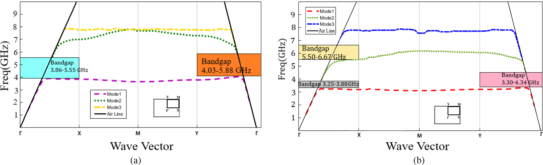
To compare the performance of the proposed ES-PDEBG structure, same-sized rectangular PDEBG structure (R-PDEBG) with a center located via is also studied. The ES-PDEBG and R-PDEBG structures are simulated in the eigenmode solution of Ansys high-frequency structure simulator (HFSS). HFSS simulation generates rectangular irreducible Brillouin-zone based dispersion diagram [Reference R23]. Both ES-PDEBG and R-PDEBG are simulated on Rogers Diclad substrate with ɛ r = 2.2, tanδ = 0.0009 with substrate height (h) = 1.57 mm. The unit cell dimensions of ES-PDEBG, as shown in Fig. 1(c), are taken as: X 1 = 13 mm, Y 1 = 6.5 mm, X 2 = Y 2 = 4 mm, X 3 = Y 3 = 3.2 mm, and d = 1.25 mm. The unit cell dimensions of R-PDEBG, as shown in Fig. 1(e) are same as the outer dimensions of ES-PDEBG, i.e. X 1 = 13 mm, Y 1 = 6.5 mm. The gap between neighboring cells and the radius of each via is respectively taken as g = 2 mm and r = 0.2 mm for both EBG structures. The dispersion diagram of R-PDEBG and ES-PDEBG is plotted in Figs 2(a) and 2(b), respectively. From Fig. 2(a), bandgap of 3.86–5.55 GHz (with bandgap bandwidth of 35.8%) from one direction (X-direction) and bandgap 4.03–5.88 GHz (with bandgap bandwidth of 37.4%) from other direction (Y-direction) is observed between mode 1 and mode 2 of R-PDEBG. However for ES-PDEBG, from Fig. 2(b), two bandgaps of 3.25–3.88 GHz (with bandgap bandwidth of 17.6%) and 5.50–6.67 GHz (with bandgap bandwidth of 19.2%) are observed from one direction (X-direction), and one bandgap of 3.30–4.34 GHz (with bandgap bandwidth of 27.2%) is observed from other direction (Y-direction).

Fig. 2. Dispersion diagram of (a) R-PDEBG. (b) ES-PDEBG.
The results of the parametric study are plotted in Fig. 3. In this figure, f cx1 and f cx2, denote the first and second bandgap center frequencies in the X-direction, respectively, and f cy1 denotes the first bandgap center frequency in the Y-direction. Bandgap center frequency variation of ES-PDEBG with the variation in inner EBG patch size, i.e. X 3 = Y 3, while keeping other parameters unchanged is illustrated in Fig. 3(a). With the increase or decrease in inner EBG patch size, the gap between the inner EBG patch and the outer eight-shape patch decreases or increases. Owing to this, the overall capacitance of the ES-PDEBG unit cell varies. It increases with the increase in the EBG patch size and vice-versa. Consequently, the center frequency of bandgaps in both directions also varies. It is observed that f cx1, f cx2 and f cy1 decrease with the increase in X 3 and vice-versa. Thus, the bandgap center frequencies can be easily tuned without changing the outer dimensions of the ES-PDEBG unit cell. Fig. 3(b), presents the bandgap center frequency variation with the variation in the gap g between the neighboring cells. Slight variations in the bandgap center frequencies with the gap g are observed.

Fig. 3. Bandgap center frequency variation of ES-PDEBG in X- and Y-directions with variation in (a) X 3. (b) Gap g.
Validation of surface wave bandgap using SML
In this section, to further validate the surface wave bandgap characteristics, simulation and measurement results of proposed ES-PDEBG structure using suspended microstrip line (SML) method [Reference Yang, Fan, Chen, She and Feng24] are presented. 5 × 5 cells of the both ES-PDEBG and R-PDEBG with same geometry parameters, as discussed in section “ES-PDEBG structure design and surface wave bandgap analysis”, are simulated using HFSS simulation software. Transmission S-parameter S 12 is calculated with one end of strip line connected to the exciting source and other end to a matched load. The simulation results of ES-PDEBG with microstrip line suspended along the x-direction and y-direction are presented in Figs 4(a) and 4(b), respectively. The simulation results of R-PDEBG with microstrip line suspended along the x-direction and y-direction are presented in Figs 5(a) and 5(b), respectively. Further, 5 × 5 cells of the both ES-PDEBG and R-PDEBG are constructed on Rogers Diclad substrate with ɛ r = 2.2, tanδ = 0.0009 and substrate height = 1.57 mm. Two such lattices are constructed for both EBG structures, one with SML along the x-direction and other with SML along the y-direction. Rogers Diclad substrate with ɛ r = 2.2, tanδ = 0.0009, and substrate height = 0.8 mm is placed above the printed EBG cells that acts as a support for SML. The Agilent Technologies PNA N5222A Network Analyzer is used to measure transmission S-parameter. Photographs of the fabricated prototypes of ES-PDEBG and R-PDEBG structures, along with their measurement results, are presented in Figs 4 and 5, respectively. From the measurement results of ES-PDEBG, two bandgaps are detected in the X-direction, while one bandgap is detected in the Y-direction with S 12 below − 20 dB. In the X-direction, first bandgap from 3.21 to 3.63 GHz with center frequency 3.42 GHz and second bandgap from 5.50 to 6.26 GHz with center frequency 5.88 GHz is observed. In the Y-direction bandgap from 3.27 to 4.11 GHz with the center frequency of 3.69 GHz is observed. From the measurement results of R-PDEBG, bandgap from 3.78 to 5.30 GHz with center frequency 4.54 GHz is observed in the X-direction, and bandgap from 3.97 to 5.62 GHz with center frequency 4.80 GHz is observed in the Y-direction. Thus, although the outer dimensions of both the EBG structures is same, the first bandgap center frequency is decreased from 4.54 GHz for R-PDEBG to 3.42 GHz for ES-PDEBG in the X-direction, and from 4.80 GHz for R-PDEBG to 3.69 GHz for ES-PDEBG in the Y-direction. Consequently, the first bandgap center frequency of ES-PDEBG is reduced by 24.7% in the X-direction and 23% in the Y-direction compared to R-PDEBG. Although the bandgaps observed from the measurement results agree well with the bandgaps observed from Brillouin-zone based dispersion diagram and simulated SML, but some discrepancies are also observed. This difference between the results is due to fabrication tolerances and using ideal infinite-periodic cells for Brillouin-zone based dispersion diagram simulation while finite (only 5 × 5) periodic cells for fabrication [Reference Peng, Ruan and Li18].

Fig. 4. Fabricated ES-PDEBG prototype photograph and transmission coefficient S 12 along (a) X-direction. (b) Y-direction.

Fig. 5. Fabricated R-PDEBG prototype photograph and transmission coefficient S 12 along (a) X-direction. (b) Y-direction.
Reflection phase characteristics of proposed EBG structure
The reflection phase characteristics of an EBG structure vary with the change in frequency of the plane wave that is incident upon it. At a particular frequency, the reflection phase attains a value of zero degree. This characteristic of EBG structure, resembles with an artificial magnetic conductor (AMC). The frequency range where the reflection phase value varies from −90° to +90° is called the reflection phase bandgap [Reference Yang and Rahmat-Samii1, Reference Yang and Rahmat-Samii2]. For a conventional EBG structure, the reflection phase characteristics are independent of the polarization state of incident plane wave. However, due to the asymmetric design of the PDEBG structure, its reflection phase characteristics are dependent on the polarization state of the incident wave. Hence, different reflection phase characteristics are obtained for x- and y-polarized incident plane waves.
To study the reflection phase characteristics unit cell of both ES-PDEBG and R-PDEBG, are simulated in Ansys HFSS. The dimensions of the unit cell of both ES-PDEBG and R-PDEBG are same, as mentioned in “ES-PDEBG structure design and surface wave bandgap analysis” section. Plane waves with linear x- and y- polarizations are incident normal to the unit cell. The reflection phase diagrams for ES-PDEBG structure and R-PDEBG structure are plotted in Figs 6(a) and 6(b), respectively. Fig. 6(a) shows that the reflection phase bandgap of ES-PDEBG is centered at 5.61 and 3.31 GHz for x- and y- polarized incident plane waves, respectively. Furthermore, Fig. 6(b) shows that the reflection phase bandgap of R-PDEBG is centered at 6.4 and 10.98 GHz for x- and y-polarized incident plane waves, respectively. Thus for the x-polarized incident plane wave, the bandgap center frequency of ES-PDEBG structure decreases by 12.34% as compared to the R-PDEBG structure. And for the y-polarized incident plane wave, the bandgap center frequency of ES-PDEBG decreases by 69.85% as compared to the R-PDEBG structure. This can be explained by carefully observing the ES-PDEBG structure. No significant perturbations are seen by electric current flowing along the x-direction in ES-PDEBG as compared to R-PDEBG; hence for the x-polarized incident wave, the bandgap center frequency of both the EBG structures is close to each other. However, the electric current flowing along the y-direction in ES-PDEBG observes significant perturbations as compared to R-PDEBG, and hence it results in longer path and reduced bandgap center frequency [Reference Yang and Rahmat-Samii9] of ES-PDEBG for y- polarized incident wave.

Fig. 6. Reflection phase characteristics of (a) ES-PDEBG. (b) R-PDEBG.
The reflection phase characteristics of the proposed ES-PDEBG structure are validated inside an anechoic chamber using measurement set up [Reference Sievenpiper, Zhang, Broas, Alexopolous and Yablonovitch21] as shown in Fig. 7(a). The measurement setup consists of two horn antennas placed next to each other, one for illuminating the test surface and another for receiving the reflected waves. The phase difference values at different frequencies are measured between two antennas with a metal plate at the test surface. The phase difference values are measured again after replacing the metal plate with 5×5 periodic lattice of ES-PDEBG structure. To compute the reflection phase of ES-PDEBG structure, the measured phase difference values obtained with the metal plate are subtracted from the phase difference values obtained with the EBG structure and then a factor of 180° is added to the phase data to account for the reflection phase of the metal plate. The reflection phase values thus obtained are plotted in Fig. 7(b). It is observed that the measurement results are in close agreement with the simulated results.

Fig. 7. (a) Measurement set up inside Anechoic chamber. (b) Measured reflection phase characteristics of ES-PDEBG.
Application of ES-PDEBG as polarization reflector
This section presents the application of ES-PDEBG as a polarization reflector. Whenever a circularly polarized wave is incident on PEC, AMC, or conventional EBG structure, the sense of polarization of the reflected wave is usually reversed, i.e. LHCP (left hand circularly polarized) to RHCP (right hand circularly polarized) and vice versa. However, the polarization of the wave reflected from PDEBG structure may be LHCP, RHCP, or linearly polarized (LP), depending upon the polarization of incident wave and the frequency of operation. The difference between reflection phases of x- and y-polarized waves plays an important role in deciding the polarization state of the wave reflected from a PDEBG structure. The absolute value of phase difference (θy - θx) versus frequency graph is plotted in Fig. 8. The graph shows that the phase difference attains a value of 180° at 3.32 GHz (f 1) and 5.67 GHz (f 2). To further study the polarization of the reflected wave, following two cases are considered:

Fig. 8. Phase difference of ES-PDEBG structure.
Case I – Response to CP incident wave: Consider that a pure RHCP wave propagating along the z-direction is incident normally upon the proposed ES-PDEBG structure. To determine the polarization state of the reflected wave the set of equations presented in [Reference Yang and Rahmat-Samii9] are discussed here. Let the incident RHCP wave $\overrightarrow {E}_{i}$ is represented as:

Thus, the wave reflected from the proposed structure can be expressed as:

The above equation can be rearranged and rewritten as:

where

and,

Here $\hat {E}_{l}$ represents the unit vector for LHCP component and $\hat {E}_{r}$
 represents the unit vector for RHCP component of the reflected wave. The axial ratio of the reflected wave can be computed as:

Putting the value of (θy − θx) equal to 180° in equation (6), it is observed that the LHCP component of the reflected wave vanishes completely and only the RHCP component is left. Since, at frequencies f 1 and f 2, (θy − θx) = 180°, thus at these frequencies the reflected wave is purely RHCP for the incident RHCP wave. Also from equation (9), the axial ratio value at frequencies f 1 and f 2 is, AR = −1.
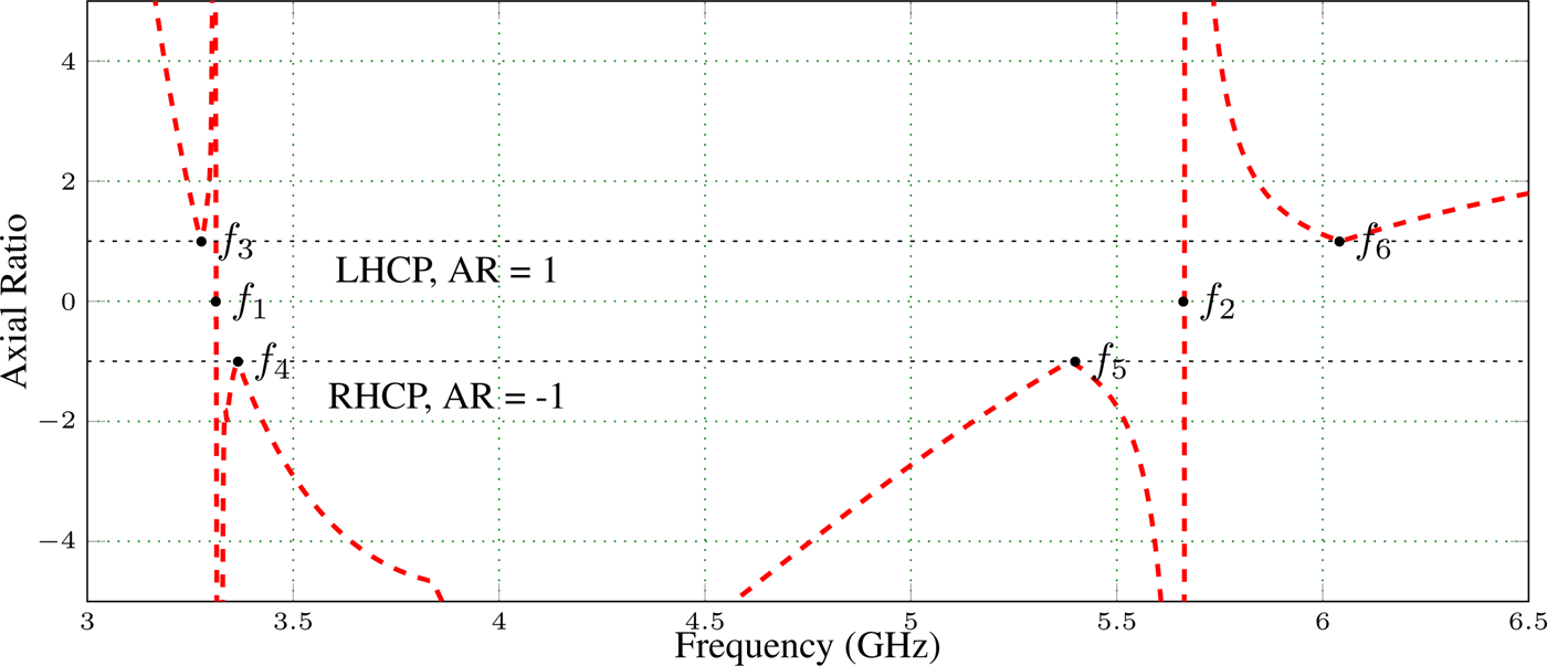
For further analysis, the LHCP and RHCP component coefficients and the axial ratio of the reflected wave are computed at different frequencies using equations (7)–(9) and the reflection phase data. The axial ratio versus frequency graph and the axial ratio in dB versus frequency graph are plotted in Figs 9 and 10, respectively. From Fig. 9, it is observed that at f 1 and f 2, i.e. at 3.32 and 5.67 GHz, the axial ratio attains a value of, AR = −1, hence the reflected wave is RHCP at these frequencies. Further the axial ratio is almost 0 dB at f 1 and f 2 as can be observed from Fig. 10. Since at these frequencies, the sense of polarization of reflected wave remains the same as that of the incident CP wave, these frequencies are called in-polarization band frequencies. There are frequency bands where the reflected wave is LHCP also, as observed from Fig. 10. Furthermore, the peaks in Fig. 10 indicate that the reflected wave is also LP at some frequency points.

Fig. 9. Axial ratio of the reflected wave in case of CP incident wave.

Fig. 10. Axial ratio in dB in case of CP incident wave.
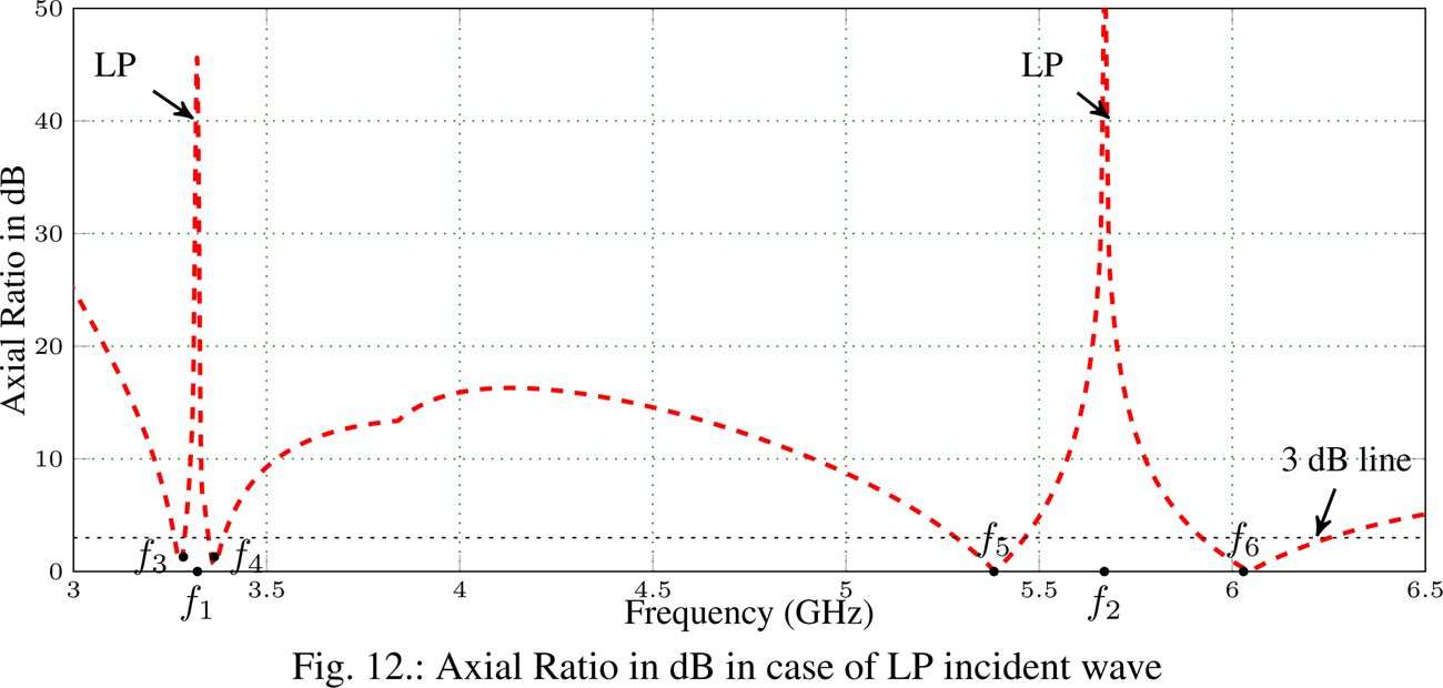
Case II – Response to LP incident wave: In this case, consider that an LP plane wave is incident upon ES-PDEBG structure. The LHCP and RHCP component coefficients and the axial ratio of the reflected wave are again computed for the LP incidence case. The axial ratio versus frequency graph and the axial ratio in dB versus frequency graph for this case are plotted in Figs 11 and 12, respectively. From Figs 11 and 12, it can be observed that at frequencies f 1 and f 2, the axial ratio is very high. This implies that at these frequencies, the LP wave is reflected. However, at these frequencies, the cross-polar component is more dominant as compared to the co-polar component. Thus at f 1 and f 2, LP conversion is achieved. From Fig. 12, it is also observed that the axial ratio is minimum at frequencies, f 3, f 4, f 5, and f 6, i.e. at 3.28, 3.37, 5.39, and 6.04 GHz. Thus, at these frequencies, the reflected waves are CP, even though the incident wave was LP. Besides, from Fig. 11 the axial ratio value is, AR = 1 at frequency f 3 and f 6; hence a pure RHCP wave is reflected at these frequencies. Similarly, the axial ratio value is, AR = −1 at frequencies f 4 and f 5; hence a pure LHCP wave is reflected at these frequencies. Consequently, with an LP incident wave, the reflected waves could be LHCP, RHCP, and transpolarized LP depending upon the frequency of operation. The LP to CP conversion property of the proposed ES-PDEBG structure can be utilized to design quad-band CP antenna using the principle discussed in [Reference Yang and Rahmat-Samii10–Reference Krishnamoorthy, Majumder, Mukherjee and Ray14].

Fig. 11. Axial ratio of the reflected wave in case of LP incident wave.

Fig. 12. Axial ratio in dB in case of LP incident wave.
Thus, from the above discussion, it is observed that the frequency (f 180), where θy − θx = 180°, plays an important role in deciding the polarization of the reflected wave. A comparison of the proposed ES-PDEBG structure with other existing PDEBG structures is presented in Table 1. From Table I, it can be observed that ES-PDEBG has two (f 180) bands, while also being more compact than many of the existing PDEBG structures. Thus, this structure can be utilized for multi-band operation in satellite communication systems to convert the sense of polarization of the received signal so as to avoid interference with the transmitted signal. Also, it can be used as stealth material for RCS reductions and in communication systems for designing quad-band circularly polarized antenna.
Table 1. Comparison of f 180 frequency and size of ES-PDEBG with other PDEBG structures.

Conclusion
In this paper, a compact size ES-PDEBG structure has been proposed. Two square slots and three vias in the unit cell of ES-PDEBG increase the overall capacitance and inductance of the unit cell. This results in lowering the surface wave bandgap and reflection phase bandgap resonant frequency. The asymmetric structure of ES-PDEBG results in different surface wave bandgaps along the orthogonal directions. Eigenmode simulations have been performed to study the surface wave bandgap characteristics. The proposed structure is fabricated, and the surface wave bandgap is measured using SML. From the measurement results, two surface wave bandgaps are observed in the X-direction, and one bandgap is observed in the Y-direction. As compared to R-PDEBG, the first surface wave bandgap center frequency of ES-PDEBG reduces by 24.7 and 23%, in X- and Y-directions, respectively. For the proposed structure the reflection phase characteristics are also studied. As compared to R-PDEBG, the reflection bandgap frequency of ES-PDEBG decreases by 12.34 and 69.85%, respectively, for x-polarized and y-polarized incident plane wave. The ES-PDEBG structure possesses unique reflector properties. It has two in-polarization bands where the sense of polarization of incident CP wave remains the same after reflection. It also has four operating bands where the incident LP wave is reflected as CP wave. The proposed structure is more compact than many of the existing PDEBG structures. Thus, for applications where multi-bandgap, polarization-dependent and compact size EBG is desired, ES-PDEBG can be an appropriate candidate.
 Priyanka Dalal received her B.Tech degree with Gold Medal in Electronics and Communication Engineering from Kurukshetra University, India, in 2007. She obtained her M.Tech degree with Honours in Electronics and Communication Engineering from Maharshi Dayanand University, Rohtak, India, in 2011. She has more than 9 years of experience in teaching B.Tech and M.Tech students. She is currently working towards her doctorate in “Applications of EBG structures in Antenna Engineering” from Guru Jambheshwar University of Science and Technology, Hisar, India. She has authored/co-authored several research papers in refereed Journals and Conferences. Her research area includes microwave communications, designing microstrip antennas, EBG structures, PBG structures, Frequency selective surfaces, Defected ground structures, UWB antennas. Her skills include modeling antennas and RF circuits using Ansys HFSS/CST Microwave Studio and their measurements using Vector Network Analyzer and Anechoic Chamber.
 Sanjeev K. Dhull received his B. Tech. degree in Electronics and Communication Engineering from Manipal University, Manipal, India, in 1996. He received his M.E. degree from the Department of Electronics and Communication Engineering, NITTTR, Chandigarh, India, in 2004. He received his Ph.D. degree from the Department of Electronics and Communication Engineering, Guru Jambheshwar University of Science and Technology, Hisar in 2013. He joined Guru Jambheshwar University of Science and Technology as Assistant Professor in Electronics and Communication Engineering Department, in 2005. Presently, he is working as a Professor in the same Department. He has served the university at various key portfolios, i.e. Chairperson of the Department, Member of Board of Studies, Member of Research Committee, etc. He has authored/co-authored more than 80 research papers in refereed Journals and Conferences. He has supervised 40 M.Tech students and currently supervising 8 Ph.D. research scholars.