I. INTRODUCTION
As a key element used for combining and dividing the power in the microwave system, many types of power dividers have been studied in the past decades [Reference Song and Xue1–Reference Cheng and Li26]. In these designs, several waveguide-based power dividers/combiners, such as ring-cavity power divider [Reference Song and Xue1], substrate integrated waveguide power dividers [Reference Eom, Byun and Lee2–Reference Zou, Tong and Yu4], radial waveguide power dividers [Reference Song, Fan and He5, Reference Hong, An and Yook6], and coaxial waveguide power dividers [Reference Xue and Song7, Reference Song and Xue8] have been studied, and some good performance is achieved. But the waveguide-based power dividers are not compact and not easy to be integrated.
Nowadays, the planar power dividers especially the dual-band power dividers draw many attentions. Although much progresses have been made on dual-band power dividers [Reference Park9–Reference Dai and Wei12], but the issue of unequal power divider is not much concerned, which was first proposed by Parad and Moynihan in 1965 [Reference Parad and Moynihan13]. The dual-band dividers in [Reference Wang and Sakagami14–Reference Wu, Zhou, Zhang and Liu16] adopt reactive components, which mean that the power divider cannot be fabricated easily and characteristic distortion of reactive components may not be avoided at high frequency. Several dual-band unequal power dividers without reactive elements are proposed [Reference Sun, Zhang and Yan17–Reference Yang and Kahng24], but these power dividers cannot operate at high frequency ratios or the operating bandwidths are narrow. In [Reference Dai and Wei12, Reference Sun, Zhang and Yan17], two resistors are adopted to increase the capacity of power handling. Two-section cascaded dual-band impedance transformers introduced by [Reference Monzon27] are adopted in [Reference Wu, Liu, Zhang and Gao18] for the impedance matching of the output ports. In [Reference Park19–Reference Chen, Liu and Li23], dual-band Wilkinson power dividers with other structures of impedance transformer are proposed. Recently, slow wave structures or CRLH phase shift lines are used to reduce the circuit size [Reference Yang and Kahng24–Reference He, Liu, Wu and Su25], but these circuits are complicated and not easy to be fabricated. A power divider presented in [Reference Cheng and Li26] has a very simple layout because the two section transformers are removed at the output ports.
In this paper, we propose a new configuration using both open- and short-ended stubs. This arrangement leads to larger frequency ratios from 2.3 to 3.7, assuming the range of the transmission-line impedance is 15–130 Ω. The analytical equations and scattering parameters are derived based on the modified even- and odd-mode analysis containing all parameters of the novel structure. Since there is one more degree of freedom in the design equations, it is flexible to choose the transmission-line impedance of the power divider if we use different impedance ratio n (when n equals to 1, the power divider becomes equal dividing). That means the proposed design method can offer flexibility in fabrication. For verification, two samples operate at 1/2.5 GHz with different values of line impedance are fabricated and tested. The measured results show matching, isolation, and amplitude balance are simultaneously achievable for the two operating frequency bands.
II. THEORY AND DESIGN EQUATIONS
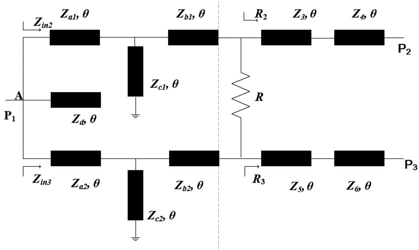
The circuit construction of the proposed dual-band unequal power divider is shown in Fig. 1. All lines have a common electrical length. The whole structure of the proposed circuit is asymmetric to achieve unequal power division. f 1 and f 2 (f 2 = m·f 1, assuming the frequency ratio is an arbitrary rational number larger than 1) are the center frequencies of the lower- and upper-bands, respectively, and f 0 is defined by (1) below, θ1 and θ2 are the electrical lengths corresponding to the two frequencies [Reference Wang and Sakagami14].
 $$f_0=\displaystyle{{f_1+f_2 } \over 2}\comma \;$$
 $$\theta _1=\displaystyle{\pi \over 2} \times \displaystyle{{f_1 } \over {f_0 }}=\displaystyle{\pi \over {1+m}}\comma \;$$
 $$\theta _2=\displaystyle{\pi \over 2} \times \displaystyle{{f_2 } \over {f_0 }}=\displaystyle{{m\pi } \over {1+m}}.$$
To obtain the design equations, the concept of the even- and odd-mode analysis is extended and applied in this asymmetric circuit. Assuming the power dividing ratio between port 3 and port 2 is equal to k Reference Eom, Byun and Lee2 (P 3/P 2 = k Reference Eom, Byun and Lee2), so the impedance R 2, R 3, Z in2, Z in3 should satisfy [Reference Wu, Liu, Zhang and Gao18, Reference Park19].
 $$Z_{in2}=k^2 Z_{in3}\comma \;$$
 $$R_2=k^2 R_3.$$
In Fig. 1, the right side of the isolation resistor R is considered as two-section transformers with the input impedance R 2 in the upper half circuit and R 3 in the lower half circuit. Based on the Monzon's theory [Reference Monzon27], the characteristic impedances of the two-section transformers can be expressed as
 $$Z_3=Z0\sqrt {\displaystyle{{k\lpar k - 1\rpar } \over {2\tan ^2 \theta }}+\sqrt {k^3+\left({\displaystyle{{k\lpar k - 1\rpar } \over {2\tan \theta }}} \right)^2 } }\comma \;$$
 $$Z_4=\displaystyle{{kZ_0 ^2 } \over {Z_3 }}\comma \;$$
 $$Z_5=\displaystyle{{Z_4 } \over k}\comma \;$$
 $$Z_6=\displaystyle{{Z_3 } \over k}.$$
Fig. 1. Proposed dual-band unequal power divider topology.
A) Even-mode analysis
In this case, appropriate sources which result in no current flows through the isolation resistor are applied to the port 2 and port 3. In addition, for the convenience of analysis, Z d is separated into two parts (Z d is equal to a parallel connection of Z d1 and Z d2), the impedance ratio between two parts is equal to k Reference Eom, Byun and Lee2. So we can obtain the following equation
 $$Z_{d1}=\lpar 1+k^2 \rpar Z_d.$$
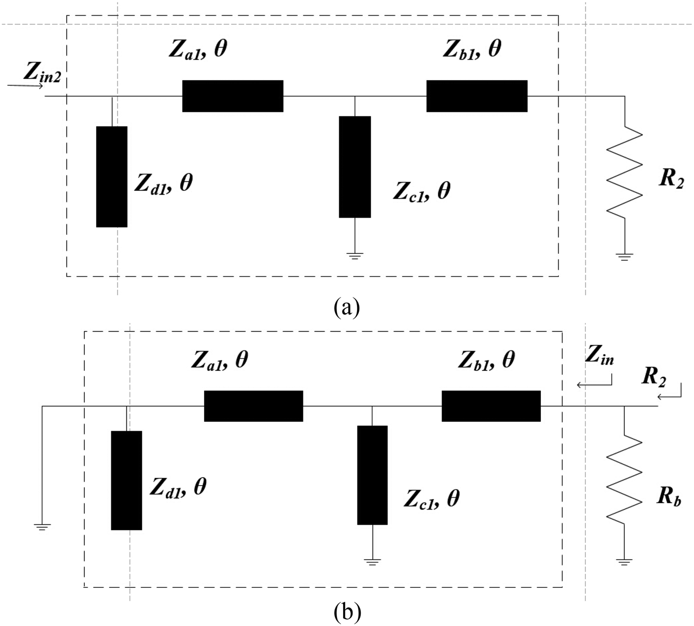
The upper half circuit and the lower side are distinguished only by the impedance level, so only the upper half circuit of even mode is depicted in Fig. 2(a).
Fig. 2. Upper half circuit of power divider. (a) Even mode. (b) Odd mode.
Because Z in2 and Z in3 should be matched to port 1, then we can get
 $$Z_{in2}=\lpar 1+k^2 \rpar Z_0\comma \; Z_{in3}=\displaystyle{{1+k^2 } \over {k^2 }}Z_0.$$
For convenience, R 2 and R 3 are assumed as
 $$R_2=kZ_0\comma \; R_3=\displaystyle{{Z_0 } \over k}.$$
The ABCD parameters of the block in Fig. 2(a) can be calculated as
 $$\eqalign{\left[{\matrix{ {{A_1}} & {{B_1}} \cr {{C_1}} & {{D_1}} \cr } } \right]& = \left[{\matrix{ 1 & 0 \cr {j{Y_1}} & 1 \cr } } \right]\left[{\matrix{ {\cos \theta } & {j{Z_{a1}}\sin \theta } \cr {j\displaystyle{{\sin \theta } \over {{Z_{a1}}}}} & {\cos \theta } \cr } } \right]\cr & \times \left[{\matrix{ 1 & 0 \cr {j{Y_2}} & 1 \cr } } \right]\left[{\matrix{ {\cos \theta } & {j{Z_{b1}}\sin \theta } \cr {j\displaystyle{{\sin \theta } \over {{Z_{b1}}}}} & {\cos \theta } \cr } } \right]\comma}$$
where
 $$Y_1=\displaystyle{1 \over 2}Y_{d1} \tan \theta\comma \;$$
 $$Y_2=- Y_{c1} \cot \theta.$$
After some algebraic manipulation, the element of the above matrix equation can be calculated as
 $$A_1=\cos ^2 \theta+\displaystyle{{Z_{a1} } \over {Z_{c1} }}\cos ^2 \theta - \displaystyle{{Z_{a1} } \over {Z_{b1} }}\sin ^2 \theta\comma \;$$
 $$B_1 = j\left({Z_{b1}+\displaystyle{{Z_{a1} Z_{b1} } \over {Z_{c1} }}+Z_{a1} } \right)\sin \theta \cos \theta\comma \;$$
 $$\eqalign{{C_1} =\,& j\left({\displaystyle{1 \over {Z_{d1} }} + \displaystyle{{Z_{a1} } \over {Z_{c1} Z_{d1} }}+\displaystyle{1 \over {Z_{a1} }}+\displaystyle{1 \over {Z_{b1} }}} \right)\sin \theta \cos \theta \cr&\!\!\!- j\displaystyle{{Z_{a1} } \over {Z_{b1} Z_{d1} }}\tan \theta \sin ^2 \theta - j\displaystyle{1 \over {Z_{c1} }}\displaystyle{{\cos ^2 \theta } \over {\tan \theta }}\comma \; }$$
 $$\eqalign{D_1 =& - \left({\displaystyle{{Z_{a1}+Z_{b1} } \over {Z_{d1} }}+\displaystyle{{Z_{d1} } \over {Z_{a1} }}+\displaystyle{{Z_{a1} Z_{b1} } \over {Z_{c1} Z_{d1} }}} \right)\sin ^2 \theta \cr & +\left({1+\displaystyle{{Z_{b1} } \over {Z_{c1} }}} \right)\cos ^2 \theta.}$$
Then, the input impedance of the circuit can be derived and expressed as [Reference Hong28]
 $$Z_{in2}=\lpar 1+k^2 \rpar Z_0=\displaystyle{{A_1 R_2+B_1 } \over {C_1 R_2+D_1 }}.$$
Assuming that the network in Fig. 2 is reciprocal and lossless, it is obvious that (11b) and (11c) are imaginary, whereas (11a) and (11d) are real. By separating the real and imaginary parts of (12), the following equations can be obtained
 $$A_1=\displaystyle{{1+k^2 } \over k}D_1\comma \;$$
 $$B_1=\lpar 1+k^2 \rpar kZ_0 ^2 C_1.$$
B) Odd-mode analysis
In the case of an odd mode, appropriate signals are applied to port 2 and port 3 to make the voltage at marker “A” equals to zero. The whole circuit can be divided into two parts by grounding the plane at a certain point. The upper half circuit is shown in Fig. 2(b), R b is part of the isolation resistor R (the other part is R c, R is equal to a series connection of R b and R c). Considering the matching condition in the right side of Fig. 2(b), we can obtain
 $$R_2=\displaystyle{{Z_{in} R_b } \over {Z_{in}+R_b }}\comma \;$$
where
 $$Z_{in}=\displaystyle{{B_1 } \over {A_1 }}\comma \;$$
From (10b), we can obtain that B 1 is an imaginary number and A 1 is real. It is very clear that Z in is an imaginary number, and so that the right side of equation (13) is a complex number because R b is a real number. But this is incompatible with the left side of (13). To satisfy (14), the following relationship must be satisfied
 $$A_1=0\comma \;$$
 $$R_b=kZ_0.$$
Substituting (11a) into (16), the generalized solution can be given by
 $$1+\displaystyle{{Z_{a1} } \over {Z_{c1} }} - \displaystyle{{Z_{a1} } \over {Z_{b1} }}\tan ^2 \theta=0.$$
Because the network is assumed to be reciprocal, the following expression is satisfied [Reference Pozar29]
 $$A_1 D_1 - B_1 C_1=1.$$
Finally, (13), (16), (18), and (19) are combined and after some algebraic manipulation, the corresponding design parameters can, therefore, be expressed by the following formulas
 $$Z_{a1}=\displaystyle{{\sqrt {k\lpar 1+k^2 \rpar } Z_0 } \over {\sin \theta \cos \theta \lpar 1+\tan ^2 \theta \rpar }}\comma \;$$
 $${\rm Z}_{d1}=\displaystyle{{\lpar 1+\tan ^2 {\rm \theta }\rpar n} \over {\lpar 1+\cot ^2 \theta \rpar \lpar 1 - 1/n\rpar }}{\rm Z}_{b1}\comma \;$$
 $$Z_{c1}=\displaystyle{{\sqrt {k\lpar 1+k^2 \rpar } Z_0 } \over {\sin \theta \cos \theta \lpar 1+\tan ^2 \theta \rpar \lpar n\tan ^2 \theta - 1\rpar }}\comma \;$$
where
 $$n=\displaystyle{{Z_{a1} } \over {Z_{b1} }}.$$
In the same manner, the characteristic impedances in the lower half circuit can be obtained and expressed as
 $$Z_{a2}=\displaystyle{{Z_0 } \over {\sin \theta \cos \theta \lpar 1+\tan ^2 \theta \rpar }}\sqrt {\displaystyle{{1+k^2 } \over {k^3 }}}\comma \;$$
 $$Z_{b2}=\displaystyle{{Z_0 } \over {n\sin \theta \cos \theta \lpar 1+\tan ^2 \theta \rpar }}\sqrt {\displaystyle{{1+k^2 } \over {k^3 }}}\comma \;$$
 $${\rm Z}_{c2}=\displaystyle{{{\rm Z}_0 } \over {\sin \theta \cos \theta \lpar 1+\tan ^2 \theta \rpar \, \lpar n\tan ^2 \theta - 1\rpar }}\sqrt {\displaystyle{{1+k^2 } \over {k^3 }}\comma \; }$$
 $$Z_{d2}=\displaystyle{{Z_0 } \over {\sin \theta \cos \theta \lpar 1 - 1/n\rpar \lpar 1+\cot ^2 \theta \rpar }}\sqrt {\displaystyle{{1+k^2 } \over {k^3 }}}\comma \;$$
 $$R_c=\displaystyle{{Z_0 } \over k}\comma \;$$
 $$R=R_b+R_c=\displaystyle{{1+k^2 } \over k}Z_0.$$
In conclusion, the parameters of this proposed unequal power divider can be calculated by (4), (20), (22), and (24). It is worth mentioning that although all the characteristic impedances of the proposed power divider are odd in θ, they have the same values of A, B, C, D at dual frequencies f 1 and f 2, respectively. That's why this proposed circuit can operate at both design frequencies.
C) Analysis of impedance values
To ensure that the resistance values of (22d) are real and positive, n > 1 is a necessary condition. From the solutions of (4), (20), and (22), all the transmission-line impedances vary with the different frequency ratio if the value of n is fixed. However, the impedance of the transmission lines is always limited to a certain range by the restriction of printed circuit board (PCB) fabrication technology. So if we choose appropriate values of n, practical line impedance can be achieved.
The characteristic impedances of the power divider calculated as a function of f 2/f 1 under different values of n when  $k=\sqrt 2 $ are shown in Fig. 3, where the values of n at different frequency ratios are listed in Table 1. It is observed that the proposed dual-band power divider can be constructed to operate over a wide range of frequency ratio (2.3–3.7) if the available transmission-line impedance values are limited to 15–130 Ω. Furthermore, the curves shown in Fig. 3 can also be used for the design charts of the proposed power divider when
  $k=\sqrt 2 $.
Fig. 3. Line impedance of the power divider versus frequency ratio with fixed power division ratio. (a) The upper part of the divider and isolation resistor, (b) the lower part and the part of two-section transformers.
Table 1. Values of n under different frequency ratios when  $k=\sqrt 2 $.

Figure 4 shows the line impedances of the power divider versus power division ratio when the frequency ratio f 2/f 1 is fixed at 2.5, the value of n is 1.8. A power division ratio up to 1:4.2 can be achieved using this proposed circuit if the line impedances are limited less than 130.5 Ω.
Fig. 4. Line impedance of the power divider versus power division ratio with a fixed frequency ratio (f 2/f 1 = 2.5) and n = 1.8. (a) The upper part of the divider and isolation resistor, (b) the lower part and the part of two-section transformers.
Table 2 shows the line impedances under different values of n in the case of f 1 = 1 GHz and f 2 = 2.5 GHz when  $k=\sqrt 2 $. It can be obtained that there are many groups of values which can be chosen to achieve the same frequency response. By choosing the value of n properly, we can tune the impedance value of the transmission line for convenient implementation. That means the proposed design method can offer flexibility in fabrication. Furthermore, there is one more transmission line of freedom to share the power and the input impedance in Fig. 2, which is the reason why this proposed circuit can operate at higher frequency ratios and power ratios.
Table 2. Line impedances under different values of n when  $k=\sqrt 2$ (in the case of f 1=1 GHz and f 2 = 2.5 GHz).
III. EXPERIMENTAL RESULTS
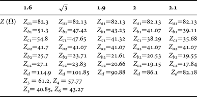
To validate the design and derived formulas, power divider A (n = 2) and power divider B (n=  $\sqrt 3 $) with the power ratio k Reference Eom, Byun and Lee2 = 2, designed to operate at 1 and 2.5 GHz were fabricated on a RF-35 substrate. The data of the substrate are ε r = 3.5, tanδ = 0.0018, thickness of the dielectric layer is 0.508 mm, and the conductor thickness is 0.018 mm. The theoretical values of the transmission-line are listed in Table 3, R = 106 Ω (for the actual implementation, the isolation resistor used in this power divider is 110 Ω).
Table 3. Measured performance comparison between the proposed and the reported ones.
aRBW: relative bandwidth, S ii and S 23<15 dB.
bPower divider A.
cNull: S ii (i = 1, 2, 3) or S 23 is larger than −15 dB.
The pictures of the two fabricated power dividers are shown in Fig. 5. The two power dividers are measured by Agilent 8757D network analyser. The simulated and measured results are presented in Fig. 6. It can be observed that there is good agreement between the simulated and measured results. Seen from Figs 6(a), 6(d) and 6(f), the measured values of ports matching are larger than 20 dB at both 1 and 2.5 GHz, indicating that there are good return losses. The isolation values are better than 28 dB for both 1 and 2.5 GHz, as shown in Fig. 6(e). In Fig. 6(b), the insertion losses of power divider A are 4.93 and 5.21 dB at 1 and 2.5 GHz, and the insertion losses of power divider B are 4.97 and 5.14 dB at 1 and 2.5 GHz. In Fig. 6(c), the insertion losses of power divider A are 2.02 and 2.28 dB at 1 and 2.5 GHz, and the insertion losses of power divider B are 1.95 and 2.23 dB at 1 and 2.5 GHz. According to the measured results, with a pass band ripple of 0.5 dB, power divider A has an operating bandwidth over 405 MHz in S 21 and 515 MHz in S 31, power divider B has an operating bandwidth of 425 MHz in S 21 and 575 MHz in S 31.
Fig. 5. Photos of the two fabricated power divider. (a) Power divider A and (b) power divider B.
Fig. 6. Measured, and simulated S-parameters of the proposed power divider. (a) S 11, (b) S 21, (c) S 31, (d) S 22, (e) S 23, and (f) S 33.
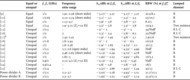
Comparison between this proposed work and the previously ones are shown in Table 3. Assuming the line impedances is range from 15 to 130 Ω. In [Reference Lee15, Reference Wu, Zhou, Zhang and Liu16, Reference Li, Yang and Yang20, Reference Li, Yang and Yang21, Reference Chen, Liu and Li23], the measured S ii (i = 1, 2, 3) or S 23 is larger than −15 dB at f 1 and f 2. Compared with [Reference Park9–Reference Cheng and Law11, Reference Wu, Zhou, Zhang and Liu16–Reference Yang and Kahng24], this circuit can operate at wider bandwidth. Compared with [Reference Park9–Reference Cheng and Wong10, Reference Wu, Zhou, Zhang and Liu16–Reference Kim, Lee and Park22], this circuit can work at higher frequency ratios. Compared with [Reference Yang and Kahng24], the proposed circuit has better performance in insertion loss and bandwidth. It can be observed that the circuit in [Reference He, Liu, Wu and Su25] has bigger insertion loss compared with the proposed circuit.
IV. CONCLUSION
In this paper, a new topology of dual-band unequal power divider has been presented. Closed-form design equations have been obtained using the modified even- and odd-mode analysis technique. The range of lower and upper band frequency ratio discussed in the paper was from 2.3 to 3.7. The proposed power divider can offer sufficient flexibility in fabrication and wide operating bandwidth. In addition, two experimental power dividers have been implemented. Good agreement between the simulated and measured results has been achieved, validating this proposed methodology.
Cong Tang was born in Shangqiu, Henan Province, China, in 1987. He received his B.S. degree in Electronic Engineering from PLA Information Engineering University, Zhengzhou, China in 2010, and is currently working toward Ph.D. degree at the University of Electronic Science and Technology of China (UESTC), Chengdu, China. His research interests include millimeter-wave and microwave devices, circuits and systems.
Yong Fan was born in 1963. He received his B.E. degree from Nanjing University of Science and Technology, Nanjing, Jiangsu, China, in 1985, and M.S. degree from the University of Electronic Science and Technology of China Chengdu, Sichuan China, in 1992. From 1985 to 1989, he was interested in microwave integrated circuits. Since 1989, he has been dedicated himself to researching and teaching on subjects of Electromagnetic Fields and Microwave Techniques for many years. His main research fields are as follows: electromagnetic theory, millimeter-wave communication, millimeter-wave, and terahertz circuits etc. Besides, he was interested in other subjects including broadband wireless access, automobile anti-collision, intelligent transportation intelligent transportation, etc. He has authored and co-authored over 130 papers.
Kaijun Song (M’09-SM’12) received his M.S. degree in radio physics and Ph.D. degree in Electromagnetic field and Microwave technology from the University of Electronic Science and Technology of China (UESTC), Chengdu, China, in 2005 and 2007, respectively. Since 2007, he has been with the EHF Key Laboratory of Science, School of Electronic Engineering, UESTC, where he is currently a full Professor. From 2007 to 2008, he was a postdoctoral research fellow with the Montana Tech of the University of Montana, Butte, USA, working on microwave/millimeter-wave circuits and microwave remote sensing technology. From 2008 to 2010, he was a research fellow with the State Key Laboratory of Millimeter Waves of China, Department of Electronic Engineering, City University of Hong Kong, on microwave/millimeter-wave power-combining technology and ultra-wideband (UWB) circuits. He was a senior visiting scholar with the State Key Laboratory of Millimeter Waves of China, Department of Electronic Engineering, City University of Hong Kong in November 2012. He has published more than 80 internationally refereed journal papers. His current research fields include microwave and millimeter-wave/THz power-combining technology; UWB circuits and technologies; microwave/millimeter-wave devices, circuits and systems; and microwave remote sensing technologies. Prof. Song is the reviewer of tens of international journals, including IEEE transactions and IEEE letters.