


I. INTRODUCTION
The rapid advancements in modern wireless communication systems have made the devices smaller and the design more intricate. Due to the miniaturization in the size of the device there often is a need for two RF traces on a PCB (printed circuit board) to cross each other while maintaining a high degree of isolation. A microwave crossover is a device that allows intersection of two transmission lines while maintaining the desired isolation for the appropriate functioning of the device. Crossover finds major application in the design of Butler matrix for antenna array. Initially, crossovers were designed using three-dimensional (3D) structures such as bond wires, underpasses, via-holes, and air-bridges [Reference Horng1–Reference Yang and Alexopoulos3]. These designs not only presented a problem in fabrication, but also exhibited considerable return loss in the passband. Considering the drawbacks in 3D crossovers, the first planar microstrip crossover was developed using a two-section cascaded branch-line structure [Reference Wight, Chudobiak and Makios4]. In [Reference Yao, Lee and Yeo5], multi-section branch-line structures for the design of crossovers have been studied and bandwidths of crossover having up to seven cascaded branch-line sections has been reported. A microstrip coupler using double-ring structure has been presented [Reference Chen and Yeo6]. In [Reference Chiou, Lai and Kuo7], the double-ring structure is extended by connecting arbitrary port-impedances to it. Crossover consisting of dual transmission lines of high impedance and different length has been proposed [Reference Ng and Pang8]. The concept of fractal geometry to design a crossover using Sierpinski carpet patch has been demonstrated [Reference Henin and Abbosh9]. A highly compact wide-band crossover of dimension 1 × 1 cm2, designed by employing only lumped elements such as capacitor and inductor has been presented [Reference Arigong10]. The design of crossover having wide-band response has been demonstrated in [Reference Tang, Lin and Chen11] by connecting a stop-band filter at each port of the proposed crossover. The band stop filter rejected the harmonics produced in the stop band of the crossover. A crossover having two-section branch-line coupler configuration with open-ended shunt stubs has been reported [Reference Liu, Yu, Liu, Li, Wu and Su12]. The crossovers reported in [Reference Yang and Alexopoulos3–Reference Liu, Yu, Liu, Li, Wu and Su12] operate at single frequency. But in the present day, microwave devices are required to function at multiple frequencies to support the current wireless standards. Several techniques to design a dual-band microwave crossover have been proposed in [Reference Lee and Pang13–Reference Maktoomi, Hashmi and Ghannouchi21]. A two-section branch-line coupler is adopted to realize a dual-band crossover [Reference Lee and Pang13]. In [Reference Yeung, Ip and Cheng14], a crossover with a tri-section branch-line structure is proposed. To facilitate dual-band operation each branch arm of the structure is replaced by a dual-band structure such as π-section. The two-section branch-line has been used to design a microwave crossover in [Reference Lin, Chu and Wong15] without any additional stubs by just increasing the length of vertical transmission line by twice its original electrical length. The inner transmission line of this crossover is replaced by a T-shaped transmission line model [Reference Lin, Chu and Wong15]. Size reduction in a dual-band crossover by 59% in area as compared with conventional crossover has been shown in [Reference Hsieh and Chi16] by using composite right/left-handed material. A dual-band crossover has been designed in [Reference Wu, Zhao, Liu and Shi17] using a cascaded structure as a replacement of the conventional branch arm. In [Reference Shao, Ren, Arigong, Li and Zhang18], the crossover derived from cascaded branch-line couplers supporting flexible frequency ratios has been presented and the derived structure was later on named as window-shaped crossover. The window-shaped crossover was modified in [Reference Tang, Lin and Chuang19] by replacing the inner transmission lines of the structure by an asymmetrical-shaped transmission line model. This design covered a wide range of frequency ratio from 2.2 to 6.89. The modified window-shape crossover was shown to be fundamentally incorrect in [Reference Sinha and De20] due to the fact that a symmetrical transmission line cannot be replaced by an asymmetrical transmission line. A dual-band crossover operating for wide-band of frequency ratios has been reported [Reference Maktoomi, Hashmi and Ghannouchi21]. This crossover was found to operate with good characteristics for the frequency ratio in between 1.35 and 4.8. In the existing literature, it is found that the crossovers can be realised only for a small range of frequency ratios.
In this paper, a new dual-band transmission line model is used to design dual-band crossovers, which can work at small as well as large frequency band ratios. The design parameters of the crossovers are obtained using closed-form equations derived analytically. Based on the design equations, the realizable small and large frequency band ratios are obtained as 1.65–2.14 and 4.1–8.76, respectively. To validate the proposed model, three examples of dual-band crossover are designed. Finally, two prototypes are fabricated and tested for the frequency ratios of 2.08 and 6. The measured return loss and isolation of the fabricated crossovers are better than 20 dB. The measured and full-wave simulated results are found in good agreement.
II. ANALYSIS OF THE DUAL-BAND TRANSMISSION LINE MODEL
The proposed topology of the dual-band cross-shaped microstrip line is depicted in Fig. 1. It is composed of two series transmission lines each of characteristic impedance Z 1 and electrical length θ1 and two open-ended shunt stubs with same electrical length of θ2 and different characteristic impedances of Z 2 and Z 3 are tapped at the center of the series lines. This dual-band microstrip line is used to replace the branch lines of the conventional crossover to produce dual-frequency characteristics. In order to compute the closed-form design equations, the ABCD matrix of the proposed topology is derived, by multiplying individual matrices of the transmission lines as follows:
 $$\left[ {\matrix{ A & B \cr C & D \cr}} \right] = M_1 M_2 M_3 M_1,$$
where
 $$M_1 = \left[ {\matrix{ {\cos \theta _1} & {jZ_1 \sin \theta _1} \cr {\displaystyle{{j\sin \theta _1} \over {Z_1}}} & {\cos \theta _1} \cr}} \right],$$
 $$M_2 = \left[ {\matrix{ 1 & 0 \cr {\displaystyle{{j\tan \theta _2} \over {Z_2}}} & 1 \cr}} \right],$$
 $$M_3 = \left[ {\matrix{ 1 & 0 \cr {\displaystyle{{j\tan \theta _2} \over {Z_3}}} & 1 \cr}} \right].$$

Fig. 1. The topology of the proposed dual-band cross-shaped transmission line.
Each coefficient of the ABCD matrix in (1) can be written as:
 $$A = D = \cos 2\theta _1 - \displaystyle{{Z_1} \over 2}\left( {\displaystyle{1 \over {Z_2}} + \displaystyle{1 \over {Z_3}}} \right)\sin 2\theta _1,$$
 $$B = jZ_1 \sin 2\theta _1 - jZ_1 ^2 \left( {\displaystyle{1 \over {Z_2}} + \displaystyle{1 \over {Z_3}}} \right)\sin ^2 \theta _1 \tan \theta _2,$$
 $$C = j\displaystyle{{\sin 2\theta _1} \over {Z_1}} + j\left( {\displaystyle{1 \over {Z_2}} + \displaystyle{1 \over {Z_3}}} \right)\cos ^2 \theta _1 \tan \theta _2.$$
The ABCD matrix of a conventional transmission line of impedance Z T and electrical length θ T can be given by:
 $$\left[ {\matrix{ {A_T} & {B_T} \cr {C_T} & {D_T} \cr}} \right] = \left[ {\matrix{ {\cos \theta _T} & {jZ_T \sin \theta _T} \cr {\displaystyle{{j\sin \theta _T} \over {Z_T}}} & {\cos \theta _T} \cr}} \right].$$
To facilitate dual-band operation, the proposed structure is imposed to provide microstrip line with characteristic impedance of Z T and electrical length of θ T at two arbitrary frequencies, i.e. A = cosθ T and B = Z T sinθ T . Therefore, the equations (3a) and (3b) can be written as:
 $$\cos 2\theta _1 - \displaystyle{{Z_1} \over 2}\left( {\displaystyle{1 \over {Z_2}} + \displaystyle{1 \over {Z_3}}} \right)\sin 2\theta _1 = \cos \theta _T,$$
 $$Z_1 \sin 2\theta _1 - Z_1 ^2 \left( {\displaystyle{1 \over {Z_2}} + \displaystyle{1 \over {Z_3}}} \right)\sin ^2 \theta _1 \tan \theta _2 = Z_T \sin \theta _T.$$
By solving the above equations, the closed-form design formulas for Z 1 and Z 2 can be obtained as:
 $$Z_1 = \displaystyle{{Z_T} \over {\tan \theta _1}},$$
 $$Z_2 = \displaystyle{{Z_1} \over 2}(1 + k){\rm tan}2\theta _1 \tan \theta _2,$$
where
 $$k = \displaystyle{{Z_2} \over {Z_3}}. $$
In order to obtain the dual-frequency operation, the magnitude of A T and B T should remain equal at two arbitrary frequencies. This implies the electrical length of the series arms and shunt stubs are computed as θ 1 and θ 2 at f 1 and mπ−θ 1 and nπ−θ 2 at f 2, respectively. Hence, the design formulas of θ 1 and θ 2 can be given as:
 $$\theta _1 = \displaystyle{{m\pi} \over {1 + p}},$$
 $$\theta _2 = \displaystyle{{n\pi} \over {1 + p}}.$$
The design guidelines for the proposed dual-band crossover working for smaller and larger frequency band ratios can be described as follows:
-
(1) Select the characteristic impedance of Z T and electrical length of θ T of the conventional transmission line.
-
(2) Set two arbitrary frequencies f 1 and f 2.
-
(3) Based on the desired frequencies, the electrical length of the series arms and shunt open stubs are computed from (8), by choosing appropriate values of m and n.
-
(4) For compactness, the value of m is chosen as 1. The smaller and larger frequency ratios can be obtained by selecting n = 2 and 1, respectively.
-
(5) Equation (6) and the values computed in former steps can be used to compute the values of Z 1 and Z 2.
-
(6) The physical parameters of the proposed structure can be evaluated at the first operating frequency f 1.
In the present days, due to the inclusion of various wireless standards/applications such as GPS, Wi-Fi, Bluetooth, WLAN, WiMAX, and LTE, dual-band RF front-end components have found significant challenges to cover closely/widely spaced communication standards. Recently, many microstrip crossovers have been developed for dual-frequency operations, which exhibit smaller band ratios [Reference Lee and Pang13–Reference Hsieh and Chi16] and large/wide-band ratios [Reference Shao, Ren, Arigong, Li and Zhang18, Reference Maktoomi, Hashmi and Ghannouchi21]. It is essential for a dual-band design to provide flexibility in terms of frequency ratio. Considering this issue, we propose a dual-frequency transmission line to cover commonly used communication standards for smaller as well as larger band ratios. The design curves to calculate the parameters of dual-band crossover operating at smaller and larger band ratios are shown in Figs 2 and 3, respectively. In both the plots, the value of k is varied to obtain realizable impedances for ease fabrication. Figure 2 shows the graphical solution for Z 1 and Z 2 versus frequency ratios (P) by choosing m = 1 and n = 2. Therefore, this solution can be used to implement dual-band crossover for smaller frequency ratios. From the plot, it is computed that the range of ratio from 1.65 to 2.14 can be devised, assuming the limitation of practical realizable impedance for microstrip technology as 20–150 Ω. Similarly, the plot of Z 1 and Z 2 versus frequency ratio (P) by choosing m = 1 and n = 1 is depicted in Fig. 3. From the graph, the range of ratio is calculated as 4.1 to 8.76, considering the same limitation of microstrip technology.

Fig. 2. Design curve of Z 1 and Z 2 as function of frequency ratio (f 2/f 1) for smaller band ratio.

Fig. 3. Design curve of Z 1 and Z 2 as function of frequency ratio (f 2/f 1) for different values of k.
III. DESIGN OF DUAL-BAND CROSSOVER
A conventional two-section branch-line coupler is modified to work as a crossover [Reference Yao, Lee and Yeo5]. The configuration of the conventional crossover is shown in Fig. 4. The required characteristic impedances and electrical lengths of the crossover are obtained as Z a = Z b = Z c = 50 Ω and θ = 90°. The proposed dual-band crossover is developed by using a cross-shaped transmission line in the place of the quarter wavelength branch-arm of the conventional crossover. To support the theoretical analysis in Section II, three examples of dual-band crossovers are designed at different frequency ratios. Finally, two prototype of dual-band crossover are fabricated and demonstrated.

Fig. 4. Schematic diagram of a two-section branch-line conventional crossover.
The design parameters for all the examples are summarized in Table 1. For example, type A crossover is designed for small band ratio, i.e. P = 2. The simulated result of the dual-band crossover operating at the global system for mobile communications (GSM) lower (0.9 GHz) and upper (1.8 GHz) bands is depicted in Fig. 5. Similarly, types B and C crossovers are developed for the frequency ratios of 4.1 and 8, respectively. Figures 6 and 7 show the circuit simulation results for types B and C crossovers, respectively. It is revealed that both channels are well isolated by over −25 dB in all examples. With the ideal transmission line, insertion losses and return losses are of 0 dB and well below −25 dB at two operating frequencies for all designs. For these designs, it is clear that the proposed dual-frequency transmission line is suitable for smaller as well as larger frequency band ratios.

Fig. 5. Frequency response of the crossover operating at 0.9 and 1.8 GHz (frequency ratio = 2).

Fig. 6. Frequency response of the crossover operating at 1 and 4.1 GHz (frequency ratio = 4.1).

Fig. 7. Frequency response of the crossover operating at 0.9 and 7.2 GHz (frequency ratio = 8).
Table 1. Design parameters of the proposed crossover for different frequency bands.

* Design parameters of the fabricated dual-band crossovers.
† Type X (smaller frequency ratio).
‡ Type Y (larger frequency ratio).
IV. MEASUREMENT AND ANALYSIS OF THE PROTOTYPE
To validate the theoretical analysis, two prototypes of dual-band crossover working for smaller (type X) and larger (type Y) frequency ratios are designed, fabricated and tested. The design parameters of the dual-band microstrip line for types X and Y are illustrated in Table 1. The type X is operating at 2.4 and 5 GHz, whereas type Y is operating at 0.9 and 5.4 GHz. The final physical layout of the dual-band crossover is shown in Fig. 8. The dimensions are computed and depicted in Table 2. The circuit size of the proposed crossovers is 0.477λ g × 0.68λ g or equivalently, 42.2 × 60.98 mm2 for type X and 0.143λ g × 0.286λg or equivalently, 35.16 × 70.32 mm2 for type Y, here λ g is the guided wavelength at f 1. The proposed dual-band crossovers are fabricated on a RT Duroid 5870 substrate of thickness 0.787 mm, with a dielectric constant ε r = 2.33. The fabricated prototypes of dual-band crossover are presented in Fig. 9.

Fig. 8. Final Layout of the proposed dual-band crossovers.

Fig. 9. Photograph of the fabricated dual-band crossovers. (a) Type X and (b) type Y.
Table 2. Computed dimensions of the physical layout for types X and Y.

The measurements of the fabricated crossovers are carried out using Rohde Schwarz Network Analyser. The return loss of the crossovers at the design frequencies are above 20 dB. The two signal paths are well isolated from each other by >20 dB at all the operating frequencies for both the prototypes. Insertion losses at f 1/f 2 are obtained as 0.33/0.72 dB for type X and 0.62/0.67 dB for type Y. The measured and simulated frequency responses of the crossovers are shown in Fig. 10 (type X) and Fig. 11 (type Y). Frequency responses depict good agreement between simulated and measured results, and both exhibit similar characteristics. The bandwidth of the fabricated prototypes is greater than 50 MHz at all operating frequencies, which is suitable for most of the applications. Table 3 shows the comparison between the proposed crossover and the current state-of-the-art crossovers.

Fig. 10. Frequency response of the crossover depicting (a) return loss, (b) isolation (S 21), (c) insertion loss, and (d) isolation (S 41).
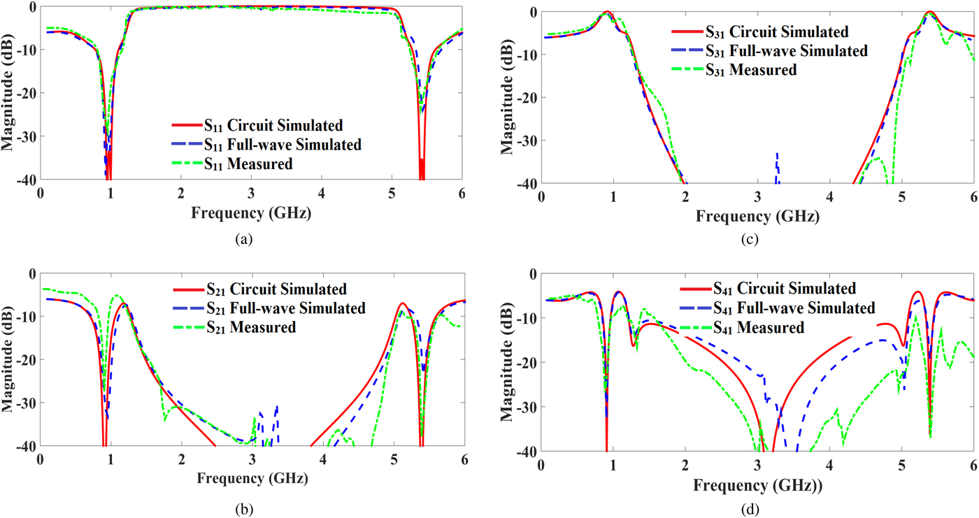
Fig. 11. Frequency response of the crossover depicting (a) return loss, (b) isolation (S 21), (c) insertion loss, and (d) isolation (S 41).
Table 3. Comparison with the current state-of-the-art crossovers.

* Type X (smaller frequency ratio)
† Type Y (larger frequency ratio).
a Estimated from the figure given in [Reference Yeung, Ip and Cheng14–Reference Maktoomi, Hashmi and Ghannouchi21], considering −20 dB reference level for S 11, S 21, and S 41.
IV. CONCLUSION
In this paper, the design of dual-band crossovers working at smaller and larger frequency ratios are presented. The derived smaller and larger band ratios for the proposed cross-shaped crossover are 1.65–2.14 and 4.1–8.76, respectively. The proposed crossover uses the cross-shaped transmission line for dual-band operation. The simulated and measured results indicate isolation and return loss above 20 dB for both the fabricated prototypes. The insertion loss in diagonal ports of each fabricated prototype is observed as <0.72 dB at the design frequency. The proposed cross-shaped structure and the design methodology described in this paper can be used for design of dual-band branch-line and rat-race coupler.
 Idury Satya Krishna received a B.Tech. degree in Electronics and Communication Engineering from the TJ Institute of Technology of Anna University in 2014. He is currently working towards Master of Design degree at Indian Institute of Information Technology Design & Manufacturing Kancheepuram. His research interest includes design of microwave passive components.
 Rusan Kumar Barik was born in Odisha, India. He received the B. Tech. degree in Electronics and Tele-Communication Engineering from Biju Patnaik University of Technology, Rourkela, India in 2012 and the M. Des. degree in Communication Systems Design from Indian Institute of Information Technology Design and Manufacturing, Kancheepuram, India in 2015, where he is currently working toward his Ph.D. degree. His research interests include design of multi-band microwave passive components and low noise amplifier for millimeter wave applications.
 S. S. Karthikeyan was born in Mayiladuthurai, Tamilnadu, India. He received the B.E. degree in Electronics and Communication Engineering from Bharathidasan University, Trichy, in 2001 and M.E. in Applied Electronics from Sathyabama University, Chennai, in 2005. He obtained his Doctoral Degree from the Indian Institute of Technology Guwahati, Assam, India in 2011. Currently he is working as an Assistant Professor at the Indian Institute of Information Technology, Design, and Manufacturing Kancheepuram, Chennai, India. His research interests include electromagnetic bandgap substrates, microwave filters, metamaterials, microwave sensors, etc.


