


Introduction
The microstrip antennas are widely used these days as they are low profile and lend themselves well with simple planar technologies while providing high front to back ratio (FBR). But, these antennas inherently have narrow bandwidth [Reference Balanis1]. The conventional bandwidth given by such antennas varies between 3 and 5% only. The other alternative to achieve low back lobe can be by utilizing a reflector behind the dipole antenna as the dipole antennas have much wider bandwidth compared to microstrip antennas.
From image theory [Reference Balanis1, Reference Balanis2], we know that when a horizontal dipole antenna is placed over a perfect electric conductor (PEC) reflector, then its image current is out of phase, thus cancelling out the effect of antenna current. Whereas, if a Perfect Magnetic Conductor (PMC) surface is used as a reflector, the image current is in the same direction and reinforces the antenna current. The high-impedance surface (HIS) is such a periodic structure which replicates the in-phase reversal property of PMC. The HIS is a periodic structure with the period of its surface texture small compared to the operating wavelength. D. Sievenpiper [Reference Sievenpiper, Zhang, Broas, Opolous and Yablonovitch3] proposed such a mushroom-like electromagnetic band-gap (EBG) structure for the first time [Reference Sievenpiper, Zhang, Broas, Opolous and Yablonovitch3]. Since then, many other structures were intended to enhance the properties of EBG structures [Reference Kovacs and Puskely4, Reference Zhang, Hagen, Younis, Fischer and Wiesbeck5]. These EBG structures are widely used to enhance antennas capabilities [Reference Yang and Rahmat-Samii6–Reference Zhu, Cheung, Liu and Yuk8].
The dipole antenna placed over a HIS can solve the problem of narrow bandwidth while giving low FBR [Reference Engheta and Ziolkowski9]. But, this system cannot provide dual-band resonance. Moreover, such a design will no longer be planar.
To solve these drawbacks, we combined the above two methodologies while preserving their advantages. We used a slotted bow-tie, complementary to the conventional dipole (Babinet theorem [Reference Balanis1]) to solve the non-planar issue of a conventional dipole antenna and the patch antenna for dual-band resonance. We integrated this bow-tie slot over a rectangular patch antenna such that it resonates for two bands while giving a wider bandwidth.
We designed a HIS to function as an artificial magnetic conductor (AMC) over 3 to 5 GHz bandwidth. In the other range of 2 to 3 GHz, it behaves as a PEC. A coplanar waveguide (CPW) fed patch antenna was designed to operate at 2.6 GHz with a bow-tie slot working at 3.5 GHz. In this manner, the HIS beneath the antenna provides a conventional PEC reflector for the patch and an AMC reflector for the bow-tie slot. To attain the circular polarization, the HIS unit cell has been designed asymmetrically by cutting slots only along one dimension. Such HIS behaves differently for the incident wave of x and y-polarization [Reference Engheta and Ziolkowski9]. This characteristic is utilized to convert a linearly polarized (LP) radiation into circularly polarized (CP) one.
In the literature, single band CP antenna [Reference Agarwal, Nasimuddin and Alphones10, Reference Yang and Rahmat-Samii11] and dual-band linear polarized antenna [Reference Zhu, Cheung and Yuk12, Reference Zhu and Langley13] have been proposed. In [Reference Yan, Soh, Mercuri, Schreurs and Vandenbosch14], a similar dual-band planar antenna with coaxial feed is proposed, but the antenna gives LP radiation. In [Reference Yi and Qu15], the mechanism to achieve CP from a rectangular cell AMC is discussed for the dipole antenna. Our design combines the planar antenna in [Reference Yan, Soh, Mercuri, Schreurs and Vandenbosch14] with the asymmetric cell AMC of [Reference Yi and Qu15] to achieve dual-band CP radiation.
This paper is categorized in the following section: 1. Proposed Antenna Design and Analysis, 2. Simulation Results, 3. Experimental Results, and 4. Conclusion. For numerical simulations, an Ansys HFSS tool is used.
Proposed antenna design and analysis
HIS unit cell design
Figure 1 shows the unit cell of the proposed HIS. The 8 × 8 array HIS structure is designed over an FR4 substrate (ε r = 4.4) with a thickness of 1.6 mm. For fabrication simplicity, the HIS cell is kept planar, i.e. without vias. To make it polarization dependent, a slot is cut in the x-direction in the unit cell such that the effective x- and y-dimensions are not the same. Due to this asymmetry, the HIS behaves differently for the incident wave of x- and y-polarization [Reference Sievenpiper, Zhang, Broas, Opolous and Yablonovitch3]. Above this surface, the proposed antenna is placed over a distance of 0.5 mm from the HIS array.

Fig. 1. HIS unit cell.
Antenna design
Figure 2 shows the bow tie slotted patch antenna. The proposed antenna is designed using an FR4 substrate (= 4.4) with a thickness of 1.6 mm and loss tangent is 0.0025. The antenna utilizes CPW feed. The dimension of patch is 20.70 × 23.50. The separation between ground and microstrip feed is 0.30 mm and the width of the microstrip line is 1.75 mm. The substrate is 60 × 60 separation between ground and patch is 14.25 mm.

Fig. 2. Bow tie slotted patch antenna.
HIS operation
HISs can be designed in many ways such as to perform different functions viz. it can be utilized to have in-phase reflection, to control the propagation of surface waves and even to have variable surface impedance depending upon the incident wave polarization. These structures are periodic in nature and to maintain their periodicity their dimensions are less than the quarter of their operating wavelength. The electrical equivalent of such structure is a parallel LC circuit. This structure provides a high-impedance boundary condition for all directions of propagation and for both kinds of polarizations. They also posse in-phase reflection rather than 180° in the case of PEC. These structures are also called AMC as they imitate the boundary condition satisfied by the magnetic conductors i.e. at the surface, the tangential component of magnetic field becomes zero which is opposite to the PEC behavior where the tangential component of the electric field is zero at the conductor boundary.
In this paper, the asymmetry of the HIS cell enables it to behave differently for the incident x- and y-polarized waves. Due to slot along the x-direction, the effective length in y dimension is reduced. Hence, for the incidence of the y-polarized wave, the structure gives zero reflection at higher frequency, which can be seen in Fig. 3 [Reference Zhang, Hagen, Younis, Fischer and Wiesbeck5]. The HIS shows + reflection phase for x-polarized and for y-polarized waves at the required frequencies. This behaviour is utilized to convert the linear polarization of the antenna into circular polarization [Reference Engheta and Ziolkowski9, Reference Liang, Sanz-Izquierdo, Parker and Batchelor16].

Fig. 3. Reflection phase (∟S11) of the unit cell (degree).
The antenna radiates a linear polarized wave that, in time-harmonic form, can be expressed as the sum of two orthogonal components in x- and y-directions. Thus, radiated electric field  $(\vec{E}_d)$ from the antenna can be expressed as,
 $$\vec{E}_d = \; \displaystyle{{E_0} \over 2}Re\lsqb {\lpar {{\hat{a}}_x + {\hat{a}}_y} \rpar e^{\,j\lpar {\omega t-\beta z} \rpar }} \rsqb $$
 The HIS gives 90° rotation to x- and − 90° rotation to y-polarized waves. Thus, the reflected electric field  $(\vec{E}_r)$ is,
 $$\vec{E}_r = \; \displaystyle{{E_0} \over 2}Re\lsqb {\lpar {{\widehat{{\,ja}}}_x-j{\hat{a}}_y} \rpar e^{\,j\lpar {\omega t-\beta z} \rpar }} \rsqb $$
 The total radiated electric field in the +z direction is superimposition of this radiated field  $\vec{E}_d$ and the reflected field
  $\vec{E}_r$.
 $$\vec{E}\; = \overrightarrow {\; E_r\;} + \overrightarrow {\; E_d} = \; \displaystyle{{E_0} \over 2}Re\lsqb {\lcub {\lpar {1 + j} \rpar {\hat{a}}_x + \lpar {1-j} \rpar {\hat{a}}_y} \rcub e^{\,j\lpar {\omega t-\beta z} \rpar }} \rsqb $$
Equation (3) shows that the radiated wave has equal magnitude for x- and y-components of the waveform while being 900 out of phase, which shows that the whole assembly of the HIS and antenna radiates CP waves.
Simulation and results
Reflection phase of HIS unit cell
The reflection phase (phase of reflection coefficient, ∟S11) of the unit cell of the HIS for normally incident wave is shown in Fig. 3. Here, x-polarized waves have 90° phase at 2.5 GHz and y-polarized waves have −90° at the same frequency. The combination produces right hand circularly polarized (RHCP) waves from equation 3. Similarly, at 3.5 GHz the phase of reflected wave for the x-polarized wave is −90° and for the y-polarized wave is 90°. A left hand circularly polarized (LHCP) wave is produced from the aforementioned combination.
Reflection coefficient of bow tie antenna
The CPW fed bow tie slotted patch antenna gives resonance at frequencies of 2.5 and 3.5 GHz. The simulated S 11 (reflection coefficient) for these frequencies are −43 and −35 dB respectively as shown in Fig. 4. The designed antenna shows a bandwidth of 75 MHz at both frequencies. The real WiMax bandwidth for 2.496–2.690 GHz is 5–10 MHz, and for (3.4–3.8) GHz is 5 MHz [17].

Fig. 4. Reflection coefficient (|S11|) of the antenna.
The conventional bow-tie antenna offers a wide bandwidth because (a) the radiation depends on the angle of bow-tie opposite to the length in standard dipole antenna [Reference Balanis1]; and (b) the volume is higher which enables the more radiation modes to fit in the structure [Reference Balanis1]. The designed antenna here has a small length and width (hence less volume). Also, it is not a conventional bow-tie antenna but a bow-tie shaped slot is cut in the microstrip patch antenna. The microstrip patch antennas are inherently narrow-band structure. Hence, the designed antenna shows narrowband behavior.
Reflection coefficient and axial ratio of bow tie antenna above HIS
Figure 5 shows a bow-tie slotted patch antenna over 8 × 8 HIS aligned with 45° shift. The separation between patch and HIS is 4.5 mm. S 11 at 2.4 GHz is around −26 and −22 dB at 3.42 GHz as shown in Fig. 6. Around 100 MHz or 4% of frequency reduction is obtained at lower frequency. A total of 2.2% or 80 MHz of frequency reduction is observed at higher frequency due to placement of the HIS below antenna. Equation (3) shows the form of field for circular polarization [Reference Yi and Qu18]. The axial ratio (AR) of less than 3 dB is achieved for both bands (Fig. 7). The AR is around 2.8 dB at 2.42 GHz and 2.8 dB at 3.42 GHz.
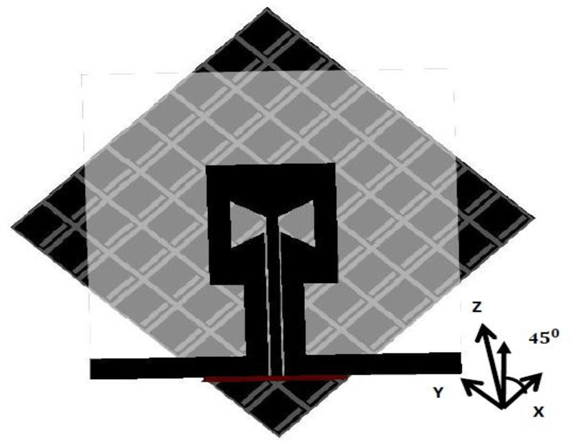
Fig. 5. Bow tie slotted patch antenna on top of the HIS.

Fig. 6. Simulated and measured reflection coefficient of the antenna (solid blue line: measured, solid red line: simulations).

Fig. 7. Simulated and measured AR of the antenna (solid red line: measured, solid black line: simulations).
Parametric study
Parametric sweep is shown in Fig. 8. As the separation between the HIS and antenna increases, the AR shifts right side and it shifts left side for a decrease in separation. The AR nearly remains constant for all sweep. The reflection coefficient with parametric sweep is observed in Fig. 9. The reflection coefficient value is shifting left and decreased as the separation between the HIS and antenna is minimized. Similar results are realized, when HIS separation is increased from 4.5 mm.

Fig. 8. Axial ratio for different gap values.

Fig. 9. Reflections from the antenna for different gap values.
Radiation pattern of bow tie slotted patch antenna
The radiation patterns are obtained for a bow tie slotted patch antenna at two required frequencies as shown in Figs 10 and 11. The RHCP pattern is realized in xz and yz planes while cross polarization is low in both planes at 2.4 GHz. For 3.42 GHz cross polarization is low i.e. RHCP while LHCP is high in xz and yz planes.

Fig. 10. Radiation pattern of the antenna at 2.4 GHz.
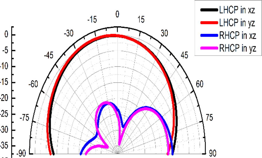
Fig. 11. Radiation pattern of the antenna at 3.42 GHz.
Experimental results
Figure 12 shows the fabricated design of the CPW fed bow tie slotted patch antenna and the polarization dependent EBG reflector. As discussed in the above section, the antenna gives the optimum performance when the gap between the two layers is 4.5 mm.

Fig. 12. Fabricated antenna and HIS.
Measured reflection coefficient of proposed antenna above HIS
Figure 6 shows the simulated and measured S 11 of the antenna. The measured result at higher frequency is shifted from the simulated however; at lower frequency, the result is close with a shift of 100 MHz. The measured reflection coefficient at 2.5 GHz is −27 dB and it is −20 dB for 3.5 GHz. The shift in frequencies is due to general fabrication and measurement errors.
Measured axial ratio of proposed antenna above HIS
The simulated and measured ARs are plotted in Fig. 12. The AR at lower frequency (2.5 GHz) is 2.5 dB, while for upper frequency (3.5 GHz) the AR is 0.9 dB. The measured AR shows 10 and 67% of improvement at lower and higher frequencies as compared to simulated result.
Measured radiation pattern of proposed antenna above HIS
Figures 13 and 14 show the measured radiation pattern of the antenna for the two resonating frequencies. The cross-polarization level in the measured pattern is comparable to the simulated pattern; however, more variations are obtained in the measured result. Deviation from simulated results is due to the feeding cable effect, fabricated and measurement errors.

Fig. 13. Measured radiation pattern of the antenna at 2.4 GHz.

Fig. 14. Measured radiation pattern of the antenna at 3.42 GHz.
Conclusion
A dual-band bow tie slotted patch antenna is designed and evaluated for WiMAX application. The antenna is fed by the CPW technique. Its low profile and circular polarization have been enabled using the polarization dependent HIS. A total of 4 and 2.2% of frequency reduction are realized at lower and higher frequency, respectively when the HIS is placed below the proposed antenna. RHCP and LHCP patterns are observed at two frequencies, respectively. The designed antenna can be used for an application where two different circular polarizations are needed in two bands. The discussed findings can also be used to alter the results according to the requirement in other applications.
 Kumar Goodwill did M.Tech in RF & Microwave from IIT Roorkee, Roorkee, India and B.Tech in Electronics & Communication Engg from Galgotia College of Engineering and Technology, Gr Noida, India. He worked as an Asst. Professor in Dept. of ECE, Sharda University, Delhi NCR, India. Currently, he is a Ph.D. scholar in Dept. of Electronics and Communication at IIT Roorkee, India. He has more than 1.5 years of teaching experience and has published several papers in International and National conferences. His area of research includes Antenna Designing, Planar Antenna Design, and UWE MIMO Antennas.
 Neha Singh received the M.Tech degree in RF and Microwave from IIT Roorkee, Roorkee, India, in 2017. Since 2017, she has been with CDAC Pune, Pune, India, where she is currently working as a Technical Officer in High Performance Computing Technologies Group. Her current research interests include Electromagnetics, Planar Antennas, High Speed System Design, and Signal and Power Integrity.
 M. V. Kartikeyan (SM'03) received the M.Sc. degree in physics, and the Ph.D. degree in electronics engineering from IIT (BHU) Varanasi, Varanasi, India, in 1985 and 1992, respectively. He has been a Full Professor with the Department of Electronics and Communication Engineering, IIT Roorkee, Roorkee, India, since 2009. His current research interests include millimeter/THz wave engineering (electron cyclotron masers, high power devices, and components), metamaterials and fractals, planar microstrip antennas and filters, MICs, and RF and microwave design with soft computing techniques. Prof. Kartikeyan is a Senior Member of IEEE, Fellow of the IET (UK), Institution of Electronics and Telecommunications Engineers (India), Institution of Engineers (India), and Vacuum Electronic Devices and Applications Society (India).


