


I. INTRODUCTION
This paper introduces a new approach to field-effect transistor (FET) capacitance modeling, which we call division by current. Although the focus is primarily on microwave FETs, the method is relevant to other types of FET devices as well, and to any kinds of devices using capacitances with multiple control voltages. In doing this, we compare it to two existing formulations, which we call division by capacitance and division by charge. Although it is possible to create an equivalence between our new formulation and a division-by-charge formulation (but not division-by-capacitance), the new one has a number of advantages:
1) It avoids many of the endemic problems of existing modeling approaches, such as charge nonconservation and inconsistency. Since it is based on a single charge region, it avoids a situation where gate charge is conserved but individual gate-to-source and gate-to-drain charges are not.
2) It is straightforward to implement.
3) Properly implemented, it is numerically efficient and stable.
4) Parameter extraction for models using the division-by-current approach is straightforward and well conditioned.
Early nonlinear FET capacitance models suffered from serious errors, which by now have been well documented. One was called the consistency problem: small-signal models were not equivalent to large-signal models operated at weak excitations [Reference Root1]. Another was charge nonconservation, in which the charge at the completion of a period of a periodic waveform was unequal to that at the beginning [Reference Statz, Newman, Smith, Pucel and Haus2–Reference Yang, Epler and Chatterjee6]. In particular, it sometimes happened that dividing the gate charge into two regions, the gate-to-drain and gate-to-source capacitances, created two nonconservative charge regions while the original gate charge was conservative [Reference Statz, Newman, Smith, Pucel and Haus4].
Capacitance, which is, after all, a linear concept, must be carefully defined in nonlinear circuits; describing nonlinear capacitances by charge functions eliminates many of the difficulties. The consistent use of charge concepts, instead of capacitance, would do much to eliminate endemic conceptual errors in nonlinear circuit modeling. For this reason, this paper focuses primarily on charge. We use the term capacitance loosely, to refer to nonlinear capacitive reactances, which are defined by charge functions.
II. THEORY
All FETs experience gate charging. The gate charge is balanced by an oppositely charged region below the gate. In junction FETs, this is a depletion region, but in HEMTs and MOSFETs, that charge region is somewhat more complex. A circuit element that models this capacitance is unusual, as it has three terminals: the FET's intrinsic source, gate, and drain (Fig. 1). As such, it is controlled by (i.e., its charge is a function of) the voltages between any two pairs of terminals. Traditionally, the control voltages are chosen to be the gate-to-source and drain-to-source voltages, V gs and V ds, respectively, but the use of gate-to-source and gate-to-drain voltages, V gs and V gd, respectively, preserves the symmetry existing in most FETs. For this reason, we shall use the latter, in most cases, in the remainder of this paper.

Fig. 1. An FET's intrinsic gate-to-channel capacitance can be viewed as a kind of three-terminal capacitor, where the terminals are those of the FET. Any pair of branch voltages defines the capacitor's charge.
The gate is one terminal of this capacitor. As such, the reactive gate current is easily defined as dQ g(t)/dt, where Q g(t) = Q g(V gs(t), V gd(t)) is the gate charge. This current is divided between the drain and source terminals in a manner that is not obvious, but, clearly, it must satisfy Kirchoff's current law; thus,
where I g, I s, and I d are the reactive components of the gate, source, and drain current, respectively.
Knowing that the gate charge balances the reactive component of the channel charge, we can determine an expression for the charge and thus the gate current. The rationale for dividing that current between the source and drain remains to be determined. Any of three approaches could conceivably be used. We call those approaches division by charge, division by capacitance, and division by current. They are explained below.
A) Division by charge
The most common treatment is to divide the channel charge into a pair of two-terminal charges, Q gs(V gs, V gd) and Q gd(V gs, V gd). This division, which seems to follow in a straightforward manner from the circuit in Fig. 1, is shown in Fig. 2.

Fig. 2. Division-by-charge formulation: the three-terminal capacitor is represented by two separate nonlinear capacitors.
To satisfy (1) we require that
where, as before, Q g(V gs, V gd) is the total gate charge. In a symmetrical device,
simplifying the formulation considerably. With this formulation, however, we must use transcapacitances in the small-signal, linear equivalent circuit. Specifically, for the gate-to-source current,
showing that a component of the gate-to-source current I s results from changes in V gd. This controlled charge source, which depends on a remote voltage, is called a transcapacitance [Reference Snider7], analogous to a controlled voltage source or current source. Similarly,
and a component of the gate-to-drain current I d results from V gs. Thus, if this formulation is used, a small-signal, linear equivalent circuit must have two capacitances and two transcapacitances. Measuring all four capacitances and transcapacitances can become a difficult problem [Reference Struble8, Reference Scheinberg and Chisholm9]. It is also possible for the individual capacitances to fail to conserve charge, even if the total gate charge is conserved; thus, an additional constraint on the division exists, which is sometimes not respected [Reference Divekar3]. Especially problematical is a charge discontinuity occurring when the drain-to-source voltage passes through zero [Reference Cheng and Hu5]. Even if such difficulties are avoided, the conversion of a single charge region into two has the potential to overcomplicate an otherwise simple situation. We examine these problems further in later sections.
B) Division by capacitance
Given the gate charge, Q g(V gs, V gd), the gate current is
We hypothesize that
which defines two nonlinear capacitances:
Again, the three-terminal capacitor of Fig. 1 has been divided into two capacitors, in a manner similar to that shown in Fig. 2, but that division is defined by the incremental capacitance, not the large-signal charge. In this case, however, the capacitor currents depend only on the time derivatives of their own terminal voltages, and not on changes in any remote voltage. The resulting small-signal equivalent circuit consists, simply, of these capacitances, evaluated at the dc bias voltages. The small-signal circuit is completely consistent with the large signal, and it requires no transcapacitances.
This approach is not convenient for harmonic-balance analysis. In harmonic-balance analysis, it is much more convenient to calculate charge waveforms and to differentiate them in the frequency domain by multiplying by jω. The simplest way to calculate (7) is to generate the time derivatives by frequency-domain differentiators in the linear subcircuit and to use the voltage derivatives as the control quantities. This doubles the number of control quantities and, in a naive implementation, causes the Jacobian matrix to become ill-conditioned. To avoid this ill conditioning, and the resulting poor convergence, the voltage derivatives must be scaled smaller and the capacitances larger by a factor approximately equal to the fundamental excitation frequency.
It is important to note that there is no underlying theoretical justification for this formulation. It is largely a conjecture, justified by its intuitive reasonableness and made attractive by its simplicity. Empirical results, including those presented later, indicate that it is indeed valid for many applications. It has been employed in widely used FET models; for example, [Reference Parker and Skellern10–Reference Hallgren and Litzenberg12].
C) Division by current
A third possibility, introduced in this paper, is to calculate the gate charge and gate current directly, then to use appropriate functions to divide it between the source and drain. Specifically, we use the division functions f gs(V gs, V gd) and f gd(V gs, V gd) in conjunction with the gate charge, Q g(V gs, V gd). Then,
To satisfy Kirchoff's current law, the division functions must have the property
for all V gs and V gd. In general, f gs approaches unity when V ds >> 0. In symmetrical FETs, when V ds = 0, f gs = 0.5 and with V ds = V gs–V gd,
An example of a set of division functions meeting these criteria, for a symmetrical FET, is
where α is a constant and g odd(x) is an odd function whose maximum value is 1.0. A promising candidate for g odd(x) might be tanh(x). If the FET is asymmetrical, (10) must still hold, but (11) and (12) in general do not. Although this is an added complication, this idea can be applied to asymmetrical FETs.
The equivalent circuit of this model is shown in Fig. 3.

Fig. 3. Large-signal equivalent circuit of a FET's channel capacitance. Q g is a charge source.
Q g is a charge source controlled by V gs and V gd. The source and drain current sources are nonlinear controlled sources, whose controlling quantity is ![]() and I/V functions are f gs and f gd, respectively.
and I/V functions are f gs and f gd, respectively.
The use of a single charge source should ease the avoidance of discontinuities caused by a switch in charge ownership at V ds = 0. Additionally, with f gs and f gd formulated as in (12), discontinuities in those functions should be easy to avoid as well. Finally, the formulation guarantees consistency between large- and small-signal formulations, charge conservation, and good convergence in simulation, as long as the three functions f gs, f gd, and Q g are smooth and continuously differentiable throughout the (V gs, V gd) space.
A seeming difficulty of this formulation is the need to evaluate the two-dimensional functions Q g(V gs, V gd) and either f gs(V gs, V gd) or f gd(V gs, V gd). The nature of the formulation makes this simpler than it at first appears. Fig. 4(a) shows the model, excluding extrinsic elements.

Fig. 4. Transformation of the division-by-current equivalent circuit. (a) Shows the circuit, according to the original concept. In (b), the gate-to-drain current source has been transformed to a pair of shunt sources. In (c), the pair of gate-to-source current sources has been replaced by its equivalent, the gate-charge capacitance. Then, the division function remains only in the drain-to-source branch, where it can be treated simply as part of the channel current.
The current source in the gate-to-drain branch can easily be transformed into two sources, one in parallel with the gate-to-source branch and another with the drain-to-source. This is shown in Fig. 4(b). Finally, in Fig. 4(c), the two controlled sources in the gate-to-source branch are simply replaced by the nonlinear gate-charge capacitor. This leaves a controlled source in parallel with the channel, which is easily absorbed into the channel-current function.
Since the division function now appears in only one place, the choice of the function is arbitrary. Any convenient function f gd(V gs, V gd) can be used, as long as the total channel current, represented by the combination of the two current sources, is correct. It seems obvious that some forms of f gd would be better than others. While f gd is real, f gd I g introduces a phase shift in the channel current that may be difficult to compensate with the channel current source I ch in a manner that is amenable to use in a circuit simulator. Thus, two branches are likely to be necessary.
D) Small-signal equivalent circuit
The small-signal gate current, i g, is simply
where the derivatives are evaluated at the bias point, (V gs0, V gd0). From (9), the small-signal reactive drain current, i d, is
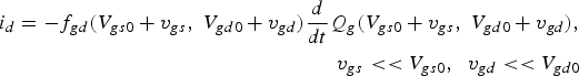
where v gs and v gd are the small-signal gate-to-source and drain-to-source voltages. Expanding f gd and Q g in Taylor series' and taking the limit as v gs, v gd approach zero gives the small-signal current,
where the derivatives are evaluated at V gs0 and V gd0.
The equivalent circuit is shown in Fig. 5; it consists of a capacitance and a transcapacitance at the gate side and a controlled source at the drain side. These elements are all easy to characterize from small-signal, Y-parameter measurements.

Fig. 5. Small-signal equivalent circuit derived from the large-signal equivalent circuit in Fig. 4(c).
This circuit is entirely consistent with the large-signal circuit; both the small- and large-signal circuits give identical results as v gs and v gd approach zero.
E) Determination of the Q g and f gd functions
It is possible to determine the Q g and f gd functions in a manner that is straightforward and numerically well conditioned. From the small-signal equivalent circuit in Fig. 5, we note that, at low frequencies, the following approximations are valid:
where G m is the magnitude and τ is the time delay of the transconductance; that is, we assume that the transconductance has the form
For practical implementation in a nonlinear simulator, it is necessary to assume τ to be constant. From (16) and (17) both ![]() and
and ![]() can be determined uniquely, and Q g can be found by path integration. Finally, f gd and τ can be selected to optimize the fit in (18) to Im{Y 21} over the required (V gs, V gd) space.
can be determined uniquely, and Q g can be found by path integration. Finally, f gd and τ can be selected to optimize the fit in (18) to Im{Y 21} over the required (V gs, V gd) space.
F) Determination of Q g from small-signal measurements
Given a general nonlinear charge function Q(V 1, V 2) we define the incremental capacitances:
The small-signal reactive current i Q(t) is found from small-signal voltages v 1(t) and v 2(t) as
where V 10 and V 20 are bias values. Clearly, C 1 can be found by setting v 2 = 0 and measuring the admittance I 1/V 1 and C 2 similarly. Then Q is found by path integration:

Q(V 1,0, V 2,0) can be set to any convenient value, usually zero, as constant charge does not affect the current in the capacitor. The path of integration is shown in Fig. 6.

Fig. 6. Values of charge are found by path integration of the capacitance in the (V 1, V 2) plane as indicated. As long as the model is charge conservative, any path may be used, although for practical reasons integrating along the axes is preferred.
In the case of FETs, V 1 represents the V gs axis and V 2 the V gd. In theory, at least one integration in the V gd direction is necessary; however, if the initial point V gs,0 is chosen well below pinch-off, there may be little charge variation with V gd, so the integration in that direction can be eliminated.
This process is applicable to all capacitance formulations. In division by charge, the two capacitances are treated separately. For the gate-to-source capacitance, ![]() and
and ![]() ; the gate-to-drain capacitance, Q gd, is treated similarly. In division by current or capacitance, the gate charge is determined directly, so
; the gate-to-drain capacitance, Q gd, is treated similarly. In division by current or capacitance, the gate charge is determined directly, so ![]() and
and ![]() .
.
G) Definition of the (V gs, V gd) space
It is worthwhile to note that a large range of the (V gs, V gd) space need not be mapped. In Fig. 7, we have plotted the FET's I/V plane in a somewhat different form from the usual; that is, we plot V gs versus V gd. This results in lines of constant V ds. The figure indicates the (V gs, V gd) space that must be considered. It is clear that a large area is not accessible, as it is limited by turn-on of the gate Schottky junction. Conversely, at voltages well below pinch-off, the gate charge varies only weakly, and linear, intermetallic capacitances dominate. Voltages above some power-dissipation limit need not be mapped, as continued operation in that region damages the device. Finally, if the device is symmetrical, only half of the accessible space (the region below the V ds = 0 contour) need be mapped.

Fig. 7. This figure illustrates the area of the (V gs, V gd) space that must be mapped, for a hypothetical device having approximately −1.0 V pinch-off. This is called the accessible region. Contours of constant V ds are shown as well. The accessible region is within the limits established by power dissipation, gate-to-channel conduction, and hard pinch-off. Furthermore, if the device is symmetrical, only the accessible region below the V ds = 0 contour must be mapped; the rest can be determined by symmetry.
For this reason, it is generally not possible to perform the contour integration as simply as is implied in Fig. 7. Invariably, multiple integration steps are necessary. Fortunately, this exercise is necessary only for determining the form of the Q g and f gd equations; once those are determined, parameters can be found by fitting to the capacitance functions, obtained by differentiating Q g, rather than the charge function.
III. CHARGE CONSERVATION
Much has been written about charge conservation in FETs, and a great deal of that material has been misleading. The requirement is often stated as
without a clear indication of the definitions of C gs and C gd. Frequently, it is assumed that these are the primary capacitances from a division-by-charge formulation; that is,
This criterion guarantees charge conservation for the total gate charge when ![]() and
and ![]() but not for the individual charges Q gs and Q gd. As such, this could be called a weak criterion for charge conservation. Conservation of the individual charges is also necessary. The criterion for charge conservation in both formulations, which we shall call the strong criterion, is given below.
but not for the individual charges Q gs and Q gd. As such, this could be called a weak criterion for charge conservation. Conservation of the individual charges is also necessary. The criterion for charge conservation in both formulations, which we shall call the strong criterion, is given below.
A) Division by charge
The conditions for charge conservation apply to a single charge source controlled by two (or more) voltages. It simply states that any change in charge is completely defined by the initial and final values of the control voltages, independent of the path taken by those voltages. For this to be the case, it is necessary and sufficient that its derivatives be continuous throughout the (V gs, V gd) space. Functions that are continuous and infinitely differentiable throughout a specified space are called analytic within that space. The charge functions we consider here need not be strictly analytic; continuity through the second derivative is sufficient. Thus, in the case of division by charge, the requirement for charge continuity, similar to (26), should be stated as
where
and similarly for Q gd. Then, both sides of (28) become
We shall call this the strong criterion for charge conservation. Any ordinary algebraic expression satisfies this property.
It should be obvious that charge conservation in the individual gate-to-source and gate-to-drain charge elements guarantees charge conservation for the total gate charge Q gs + Q gd. Thus, this strong criterion satisfies the weak criterion in all cases. The weak criterion simply states, for the total gate charge,
This has little practical value, however, and does not guarantee charge conservation for the individual Q gs and Q gd charge functions.
Charge nonconservation is strong evidence of model invalidity, as real capacitors always conserve charge. Additionally, it creates practical difficulties in circuit simulation. Time-domain simulators sometimes carry capacitor charge as a variable, and if a capacitor does not conserve charge, numerical overflow quickly occurs. In harmonic-balance simulation, the existence of a finite charge difference between the beginning and end of a waveform period results in the appearance of dc current in the capacitor. If the weak criterion, but not the strong, is satisfied, no dc gate current is created, but dc currents in the individual gate-to-source and gate-to-drain capacitances are possible. Satisfying the strong criterion prevents this.
B) Division by current
The division-by-current formulation is based on a single charge function, so charge conservation requires only that the function satisfies the fundamental requirement,
throughout the entire (V gs, V gd) region.
For a number of mostly obvious reasons, f gs and f gd should also have continuous derivatives throughout this region as well. As long as Kirchoff's current law is satisfied, however, discontinuities in the f gs and f gd functions do not affect charge conservation.
IV. THE “CHARGE OWNERSHIP” PROBLEM
Charge nonconservation is likely to occur in division-by-charge models when V ds(t) passes through zero. In most model formulations, the Q gd and Q gs charge functions are interchanged, as are their control voltages, when V ds changes its sign.
The case is made in [Reference Statz, Newman, Smith, Pucel and Haus4] that, as the V ds(t) passes through zero, Q gs and Q gd are interchanged. The change in “charge ownership” by the gate-to-source and gate-to-drain capacitances results in nonconservation of the individual charges. This point is illustrated by tracing the FET charge through a closed path in the (V gs, V gd) plane, including the V ds = 0 point. The example shows that, while total gate charge is conserved, the individual charges are not.
If the charge functions are individually conservative (i.e., in the strong sense) and the device is symmetrical, Q gs = Q gd at V ds = 0 of necessity. Then, a change in charge ownership does not affect the drain or source currents. Discontinuities in the derivatives of these functions at V ds = 0 are still possible, however, and may be subtle. Such difficulties still may lead to convergence failure in harmonic-balance analysis.
A lack of appreciation of this point has resulted in model behavior that is not physically correct. An example is the widely used BSIM3 model for MOSFETs [Reference Cheng and Hu5]. This model treats the gate charge as a single element, but then employs a clumsy technique for partitioning it between the drain and source. Documentation for the model frankly admits that some of the partitioning methods result in nonphysical drain- and source-current impulses occurring as V ds(t) passes through zero. This is a strong indication of a charge-ownership problem.
V. VALIDITY OF DIVISION BY CAPACITANCE
We noted that the division by capacitance approach is based on the hypothesis in (7). It seems likely to be valid when the device is in current saturation, as C gd is dominated by intermetallic capacitances and shows little variation with V gd. In the device's linear region, however, it is not at all clear that this hypothesis is valid; thus, measurements on the device in that region should clarify the matter.
Consider the device in a common-gate configuration, as shown in Fig. 8, with C ds and all terminal parasitics removed. We evaluate the device at V ds = 0, which is likely to be the worst case.

Fig. 8. Dependence of i s on v gd or i d on v gs can be determined from Y-parameter measurements of the device in common-gate configuration.
In this case, if the small-signal i s varies with v gd, indicated by a nonzero value of Y 12, a transcapacitance, C gsm in the figure, must exist.
Figure 9 shows measured values of Y parameters of a small-signal HEMT, a Triquint foundry device, biased at V ds = 0. At values of V gs close to zero, there is a clear indication of a transcapacitive effect in Y 12. As V gs becomes more negative, however, but still remains above the threshold voltage, the effect disappears quickly. Further measurements show that it disappears rapidly with V ds as well. It appears that the division by capacitance approach may be useful for circuits in which the device remains in saturation, or dips only lightly into its linear region. If the device is operated primarily in its linear region, as is the case in switches and FET resistive mixers, this approach to modeling probably is not useful.

Fig. 9. Measurements of Y parameters at V ds = 0 and various values of V gs. The positive imaginary part of Y 12 is a clear indication of a transcapacitance. Note that at V ds = 0, Y 12 = Y 21. The frequency range is 0.1–26 GHz.
VI. EQUIVALENCES IN THE FORMULATIONS
All formulations are equivalent, in the sense that they derive from a single gate charge, Q g(V gs, V gd). In division by charge, this quantity is divided into two charges, Q gs and Q gd, where Q g = Q gs + Q gd, whose derivatives define the source and drain reactive currents. In division by capacitance, the partial derivatives of Q g(V gs, V gd) define those currents, while in division by current, they are split by a pair of separate functions, f gs(V gs, V gd) and f gd(V gs, V gd).
A) Division by charge and division by current
Equivalence between division by charge and division by current can be shown as follows. We consider the case of the gate-to-source current; the drain current follows by analogy. The current is
Straightforward algebraic manipulation gives
showing that f gs(V gs, V gd) and, therefore, f gd(V gs, V gd) can be derived directly from terms of the division-by-charge formulation. This implies that
which is the definition of the capacitance C gs in both the division-by-current and division-by-charge small-signal equivalent circuits.
Since these two approaches can be equated algebraically, one can legitimately question the need for the division-by-current formulation. That formulation has the advantage of helping to avoid many of the previously described pitfalls in FET modeling. In addition, it has significant advantages in numerical conditioning in parameter extraction and in its implementation in a simulator.
B) Division by charge and division by capacitance
Again, for simplicity we consider the gate-to-source current. For the division-by-charge case, we have
For the division-by-capacitance case,
In (36) the current is a function of the V gs and V gd time derivatives, while in (37) it is a function of the V gs derivative only. Since V gs and V gd are independent quantities, it is clearly impossible to equate the two approaches.
VII. PARAMETER EXTRACTION
From an analysis of Fig. 5 we obtain
From these, the derivatives of the charge are determined unequivocally, and the charge function is found by path integration. An appropriate value for τ is selected and f gd determined accordingly. Finally, f gs is found from (10). Drain-to-source capacitance C ds is found from Y 22. Since these quantities are determined from low-frequency measurements, parasitic inductance, and series resistance affect the extraction minimally. In any case, these can be removed by well-known means [Reference Parker and Mahon15–Reference Aaen, Bridges, Pla and Wood18].
Figure 10(a) shows the small-signal circuit as implemented in a circuit simulator, and Fig. 10(b) shows the results of fitting to Y parameters of a Triquint foundry device, at moderate frequencies. The f gd function behaved as expected, and a constant value of τ fit the data accurately.

Fig. 10. Small-signal equivalent circuit (a) and Y-parameter fitting (b) of the model.
VIII. CONCLUSIONS
We have shown that existing FET capacitance formulations are based on one of two fundamental approaches, which we call division by capacitance and division by charge. We have additionally proposed a third formulation, called division by current, which has significant advantages compared to the former two.
One central purpose of this study was to introduce the division-by-current formulation and to compare it to the others. It was determined that this formulation is practical, and it has significant advantages in parameter extraction and, perhaps, simulation efficiency and numerical conditioning. As it can be made equivalent to the division-by-charge formulation, it has many identical properties.
We have also examined a number of matters regarding these formulations, which, in our view, either have never been clearly addressed in the literature or are frequently confused. Finally, we have evaluated the characteristics, validity, and practicality of the three formulations. We found that the division-by-charge and division-by-current formulations are quite general. The division-by-capacitance approach, however, may be invalid for resistive FET applications.
ACKNOWLEDGEMENTS
This work was supported by Ericsson AB and Chalmers University of Technology, Göteborg, Sweden.
 Stephen Maas received BSEE and MSEE degrees in Electrical Engineering from the University of Pennsylvania in 1971 and 1972, respectively, and a Ph. D. in Electrical Engineering from UCLA in 1984. He has been involved in research, design, and development of low-noise and nonlinear microwave circuits and systems at the National Radio Astronomy Observatory (where he designed the receivers for the Very Large Array), Hughes Aircraft Co., TRW, the Aerospace Corp., and the UCLA Department of Electrical Engineering. Subsequently he worked as an engineering consultant and founded Nonlinear Technologies, Inc., a consulting company, in 1993. He is currently Chief Scientist of AWR, Inc.
Dr. Maas is the author of Microwave Mixers (Artech House, 1986 and 1992), Nonlinear Microwave Circuits (Artech House, 1988; second edition 2003), The RF and Microwave Circuit Design Cookbook (Artech House, 1998), and Noise in Linear and Nonlinear Circuits (Artech House, 2005). From 1990 until 1992 he was the editor of the IEEE Transactions on Microwave Theory and Techniques and from 1990–93 was an Adcom member and Publications Chairman of the IEEE MTT Society. He received the Microwave Prize in 1989 for his work on distortion in diode mixers and the MTT Application Award in 2002. He is a Fellow of the IEEE.


