


I. INTRODUCTION
Satellite COTM (communication on the move) terminals require both transmitting and receiving antenna systems with the capability to track different targets during motion with high resolution and low probability of interception. Electronically steerable antennas offer many advantages over conventional mechanically scanned arrays such as fast scanning rate, low weight, and beam shaping capability. The electronic beam steering is realized by using variable loads, phase shifters or true time delay (TTD) networks to control the phase of the individual radiating element of the antenna array without any mechanical motion [Reference Schoebel1]. MEMS represent an extremely attractive alternative for the realization of TTD and programmable phase shifters due to the low loss, low-power consumption, and excellent linearity compared to the traditional monolithic microwave integrated circuit. In recent years a very large number of electronically reprogrammable MEMS phase shifters and TTD have been presented in literature showing superior performance in different frequency ranges [Reference Kim2–Reference Sundaram5]. Such a technology, however, presents significant reliability issues that have prevented so far the actual integration of MEMS in telecommunication systems. Most critical aspects reside in the manufacturing and packaging process stability and most often depend on the specific technology and design. For these reasons it is difficult to identify and select in advance the most promising MEMS switch typology from the large variety that have been developed up to now (i.e. cantilever/clamped–clamped beams, ohmic/capacitive contact, shunt/series, in-line/broadside configuration, etc.). As an example, cantilever beams show several advantages with respect to clamped–clamped bridges, such as lower loss and improved robustness to temperature variation. On the other hand, cantilevers are intrinsically more sensitive to process stress gradient variations and they can show low restoring force that make them more prone to remaining in down position in case of dielectric charging or micro-welding phenomena.
This paper presents the design, manufacturing, and testing of three K-band 5-bit MEMS phase shifters to be used in a phased array antenna for satellite COTM terminals. The three designs, namely PS1, PS2, and PS3, are based on the same hybrid architecture (switched and loaded lines) but differ in the typology of single pole single throw (SPST) switch utilized (cantilever or clamped–clamped beams) and in the RF junctions (SP2T or SP4T) as described in Section 2. They have been monolithically manufactured on 200 µm thick high resistivity silicon substrate by using the well-established eight-mask FBK MEMS process [Reference Farinelli6]. Section 2 presents the design of the three MEMS phase shifters together with full-wave simulations. The manufacturing and experimental results of the MEMS SPST cantilever and air-bridge switches are shown in Section 3. Section 4 presents the RF performance obtained for the different phase shifter single bits as well as the full devices. Finally Section 5 shows the design, simulation, and measured RF performance of the developed low-cost one-level SMT package.
II. PHASE SHIFTER DESIGN
The three-phase shifters, PS1, PS2, and PS3, are based on a similar hybrid architecture consisting of the combination of switched line and loaded line topologies. They have been designed to provide a programmable phase shift in the range 0–360° in the 20.2–21.2 GHz frequency band. The most significant 4 bits are realized by using switched microstrip lines and series ohmic MEMS switches whereas the less significant bit consists of a microstrip line section loaded by shunt capacitive MEMS devices. The three-phase shifters differ in the typology of the SPST switch utilized and in the RF junctions that have been developed to drive the signal into the desired path.
PS1 is based on clamped–clamped beam MEMS switches and SP2T junctions [Reference Bastioli7]. The designs adopted for the realization of the air-bridge series ohmic and shunt capacitive switches are similar to the ones presented in [Reference Farinelli6] that already demonstrated high performance in terms of both RF response and reliability. The main difference with respect to such a tested design resides in the removal of the dielectric on top of the fixed electrodes in order to mitigate the dielectric charging phenomena [Reference Mardivirin8]. Mechanical stoppers have been integrated in the fixed electrodes in order to avoid their contact with the movable beams when activated. In addition, mechanical stoppers have been deposited on the microstrip line below the shunt capacitive switch central part in order to obtain a repeatable C on/C off ratio of 5. No higher ratios are needed indeed for the realization of the 5th bit, which provides the 11.25° phase shift at the center frequency 20.7 GHz.
PS2 is based on cantilever beams (size: 90 µm ×220 µm) and SP2T junctions; also in this case the dielectric-free pad solution has been adopted. Finally, PS3 is based on the same cantilever switches as PS2 and SP4T junctions to realize the first 4 bits whereas the loaded line bit is identical to PS2. By using a SP4 T building block the same phase shift states are achieved with a halving of the number of series switch to be crossed by the RF signal in the input–output path (four switches instead of eight in the case of 4 bits).
Figure 1 shows the photos of the three-phase shifters whereas Fig. 2 presents zoomed images of the different junctions. The space occupation of PS1 is 11.35 × 3.2 mm2, of PS2 is 6.5 × 3.2 mm2, and of PS3 is 6.5 × 4.5 mm2. Note that the dimensions of PS3 could be significantly reduced by adding additional meanders to the transmission lines. On the contrary the dimensions of PS1 can hardly be reduced since they are limited by the utilization of the pretty large broadside clamped–clamped MEMS switches.

Fig. 1. Photos of the 5-bit K-band MEMS phase shifters: (a) PS1 (clamped–clamped and SP2T design), (b) PS2 (cantilever and SP2T design), and (c) PS3 (cantilever and SP4 T design).

Fig. 2. Zoomed view of the different junctions adopted in PS1 (a), in PS2 (b), and PS3(c).
Full-wave simulations (Fig. 3) of every single bit have been performed (by using ADS Momentum [9]) in order to avoid off path resonances in the frequency band of interest [Reference Bahl and Bhartia10]. Such resonances are due to the non-zero off-state capacitance of the MEMS switches (about 5 fF for clamped–clamped design and 9 fF for cantilevers) that lead to resonances clearly visible in the simulations (Fig. 3(c), S21 dips at 19 and 24 GHz). In the SP2 T-based design such resonances have been widely moved out of band by properly dimensioning the reference paths of every line bit. On the other hand, the SP4T-based design requires the simultaneous optimization of the four transmission paths and a narrowband design around the 20.2–21.2 GHz has been obtained. Return loss better than 18 dB and insertion loss better than 0.6 dB have been obtained for all designs in the operating frequency band 20.2–21.2 GHz (the simulations do not account for the switch contact resistance). The phase shift is extremely linear and a phase error is less than 2° for all designs.

Fig. 3. Full-wave simulations of the single bits: (a) PS1 (clamped–clamped and SP2T design), (b) PS2 (cantilever and SP2T design), and (c) PS3 (cantilever and SP4T design).
III. MANUFACTURING AND SPST SWITCH EXPERIMENTAL RESULTS
The 5-bit phase shifters and all their building blocks (single bits, SP2T, SP4T, and SPST switches) have been monolithically manufactured on 200 µm thick high resistivity silicon substrate (4″) by using the well-established eight-mask FBK RF MEMS process [Reference Farinelli6]. The process allows the electro-deposition of two gold layers of different thicknesses for highly complex movable bridges and microstrip lines. The air bridges are realized without the need of any planarization steps by using a 3 µm thick photoresist as sacrificial layer. The bridge release is done with a modified plasma ashing process in order to avoid sticking problems. The bias network is realized by depositing a high resistivity 0.63 µm thick poly-silicon layer covered with silicon oxide for isolating the DC from the RF lines. This layer is also used for realizing the stopping pillars used in the capacitive switches and the contact bumps for the ohmic switches. The process allows the monolithic manufacturing of both ohmic and capacitive switches. Low temperature oxide is used as dielectric for capacitive switches as well as MIM capacitors. A third gold layer is deposited for the realization of low resistance metal-to-metal electro-mechanic contacts for ohmic switches. The mechanical stoppers integrated in the switch fixed electrodes have been realized by stacking polysilicon, dielectric and gold layer in order to reach a stopper thickness about 0.55 µm higher than the electrode thickness. This prevents the MEMS membrane from contacting the dielectric-free fixed electrodes when activated.
Figure 4 shows a photo of the manufactured MEMS wafer and illustrates how the different devices have been arranged in the wafer: the top part has been occupied by a high number of repetitions of the SPST switches constituting the phase shifters (included for reliability test purposes); the central part consists of PS1 and PS2 phase shifters to be diced and packaged; the bottom part is occupied by the three-phase shifters PS1, PS2, PS3 and their single bits to be tested on-wafer.

Fig. 4. Photo of the manufactured 4″ HR silicon wafer.
A batch fabrication of 20 wafers has been completed; the RF characterization has been performed sparsely on different wafers in order to monitor the measurement repeatability and yield.
The cantilever and air-bridge ohmic SPST switches have been realized in coplanar technology (Figs 5(a) and 5(b)) and characterized in the 5–30 GHz frequency band (Fig. 5(c)). High and repeatable performance was measured for both devices. The air-bridge series ohmic switch shows an off-state isolation better than 20 dB and an insertion loss better than 0.4 dB up to 30 GHz. On the contrary, the cantilever switch shows an isolation better than 12 dB and an insertion loss better than 0.2 dB in the same frequency range. These correspond to an off-state capacitance of 5 and 9 fF and an on-state resistance of 1.8 and 0.9 Ω for the air-bridge and cantilever designs, respectively. As expected the cantilever shows half loss and half isolation with respect to the air-bridge configuration due to the single contact compared to the double contacts of the clamped–clamped devices. Note, however, that both switches are based on the same contact mechanism and material, consisting of the application of a controlled force (not dependent on the voltage applied) on multiple gold bumps. For both designs it has been observed that the mechanical stoppers introduced to realize the dielectric-less pad switches do not lead to any variations of the RF performance with respect to the standard design (without stoppers). On the contrary the dielectric-free pad solution has significantly reduced the dielectric charging phenomena and no variation of the pull-in voltage is recordable when cycling the switches [Reference Tazzoli11]. Cycling at low RF power of both switches has shown no degradation of the ohmic contact at least up to 107 cycles for both devices. Additional tests are going on in order to better understand and improve the contact mechanism, i.e. by optimizing the number and shape of the contact bumps as well as replacing the gold-to-gold contact with harder materials. Preliminary thermal tests on similar designs have shown improved robustness of cantilever with respect to air bridge due to the single clamping which releases the stress introduced by the different CTE factors of silicon substrate and gold membrane.
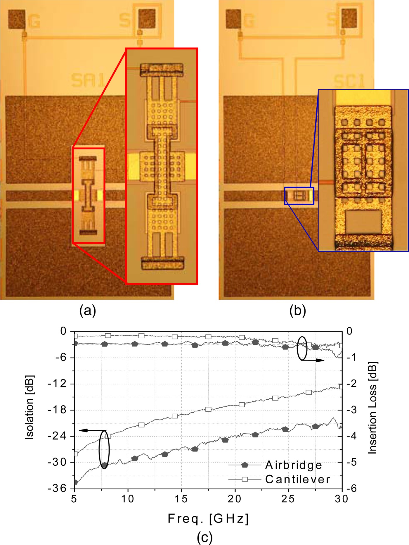
Fig. 5. Photos and performance of the MEMS SPST switches constituting the phase shifter: (a) series ohmic air-bridge switch, (b) series ohmic cantilever switch, and (c) measured isolation (left y-axis) and insertion loss (right y-axis) of the two switches. The measurements include the 1.3 mm long CPW line.
For the capacitive load an off-state capacitance of 55 fF and an on-state capacitance of 270 fF were measured, resulting in a C on/C off ratio equal to 4.9 (Fig. 6). This value is in very good agreement with the theoretical one: the down-state capacitance of such a device is indeed insensitive to dielectric roughness or bridge shape factors due to the stopping pillars that lead to an almost ideal metal-air-metal capacitor.

Fig. 6. Photo (a) and measured performance (b) of the MEMS shunt capacitive load. Transmission parameter S21 for the switch in up-state and down-state. The measurements include the 1.3 mm long CPW line.
IV. PHASE SHIFTER EXPERIMENTAL RESULTS
The three-phase shifters and their single bits have been characterized on-wafer in the 15–25 GHz frequency band using coplanar RF microprobes. In order not to increase the manufacturing complexity, via-less microstrip-to-coplanar interconnections have been designed resulting in pretty large and narrowband transitions. In order to de-embed the measurements from the contributions of such transitions, a specific TRL calibration kit has been designed, realized on-wafer, and utilized for the phase shifter characterization.
The measured performances of the single bits are presented in Fig. 7. A return loss better than 18 dB has been measured for all bits of the three designs in the frequency band of interest 20.2–21.2 GHz. However note that in case of SP2 T-based designs PS1 and PS2 low return loss is obtained in a significantly large frequency band with respect to PS3. The insertion loss is better than 1.3 dB for the clamped–clamped design PS1 and better than 0.7 dB for both cantilever-based designs PS2 and PS3.

Fig. 7. Measured performances of the single bits: (a) PS1, (b) PS2, and (c) PS3.
The phase response of the single bits of the three designs is shown in Fig. 8 and summarized in Table 1. The phase error is on average below 2° in all bits (Table 1) with the exception of the 45° lines of PS3 that showed an anomalous behavior (positive phase error of 8.63°). Such phase error is very repeatable over bits belonging on different wafers. This suggests an error in the simulation that can be corrected in the next design cycle. Note that in case of SP2T-based designs PS1 and PS2 the phase shift is linear over a very wide frequency band, larger than the measured 15–25 GHz. On the contrary the PS3 single bits present off-paths resonances that limit the phase linearity to the 20–22 GHz frequency band. Such resonances were pretty well predicted by the full-wave simulations shown in Fig. 5(c).

Fig. 8. Measured phase shift of the single bits: (a) PS1, (b) PS2, and (c) PS3.
Table 1. Single bit phase error at 20.7 GHz.

The on-wafer measurements of the full 5-bit phase shifters are shown in Fig. 9 for the shorter and longer paths and summarized in Table 2. The three designs showed return loss better than 15 dB for all states. However note that as expected the 15 dB bandwidth is obtained in a significantly larger band for the PS1 and PS2 designs with respect to the PS3. The average insertion loss is about 3.5 dB for the clamped–clamped design PS1, 2.2 dB for PS2, and 2.1 dB for PS3.

Fig. 9. Measured performances of the 5-bit MEMS phase shifters (shorter and longer paths): (a) PS1, (b) PS2, and (c) PS3.
Table 2. Comparison of the three-phase shifters performance.

Comparison between PS1 and PS2 clearly indicates that significantly higher performance can be obtained by using the cantilever design with respect to air bridge. This is indeed not only due to the halving of the contact resistance but also to the shorter RF line lengths allowed by the series in-line cantilever design (PS1 and PS2 lengths of 11.8 and 6.5 mm, respectively). On the contrary comparing PS2 and PS3 performance, it seems that in both designs the losses are not dominated by the cantilever contact resistance but by the microstrip line loss. The average insertion loss of PS2 and PS3 is very similar even though PS3, in principle, could be optimized for a more compact design and consequently lower loss. The insertion loss variation of the different phase shifter states is 0.5 dB for PS1, 0.4 dB for PS2, and it is around 1 dB for PS3. Such a significant variation for PS3 can be attributed to the higher return loss of some states as well as higher coupling between different paths. Proximity effects and off-state resonances can indeed worsen the RF performance of some PS3 phase shifter states. A more accurate optimization of the single paths as well as the reduction of the off state MEMS switch capacitance can most likely reduce such effects and enlarge the phase shifter bandwidth. However, these results indicate that the SP4T-based design requires higher design efforts since it is intrinsically more sensitive to proximity and coupling effects.
Looking at the performance obtained for the three MEMS phase shifters monolithically manufactured on HR silicon substrate the best trade off in terms of high compactness, low loss, low design complexity, and high switch robustness seems to be provided by the SP2T-based cantilever design PS2.
V. PACKAGE DESIGN AND CHARACTERIZATION
A low-cost packaging solution has been developed in order to test and integrate the phase shifters PS1 and PS2 into a phased array antenna by using automatic surface mounting equipment. Laminate RT Duroid 5880 [12] was chosen as a substrate since it is a good trade-off between high RF performance and low cost. Five layers, 254 µm thick each, have been necessary to complete the one-level MEMS package. Wire bonding techniques have been adopted to interconnect the phase shifter with the RF signal line in the package. Three parallel bonding wires (25 µm in diameter) have been used for each interconnection in order to reduce the total series inductance introduced by the wires. A transition with two via-holes has been designed to bring the RF signal from the intermediate laminate layer into the external bottom surface thus allowing surface mounting solutions. Capacitive pads have been patterned between the two via-holes stages in order to compensate for the parasitic inductance generated from the vias. It has been verified that nevertheless the utilization of three parallel bonding wires their inductive effect would strongly deteriorate the return loss of the interconnection and consequently of the K-band phase shifters. In order to obtain a good matching in a very wide frequency band, inductive–capacitive (L–C) matching sections have been then designed and added in the silicon die as well as in the package side. Such sections have been accurately dimensioned starting from their equivalent lumped element circuit and then optimized by using the full-wave 3D simulator CST Studio [13]. The 3D layout of the single die-carrier transition is shown in Fig. 10.

Fig. 10. 3D-layout of the one-level plastic package single transition: (a) prospective view and (b) side view.
In order to evaluate the package RF characteristic it has been analyzed a 50 Ω line of the same length of the phase shifters packaged by using a row interconnection or the optimized one. The latter includes the L–C compensation sections. The analyzed structures consist of an 11.55 mm long 50 Ω microstrip line (on HR silicon substrate) wire-bonded and packaged on the one-level Duroid and mounted on a Teflon printed circuit board (PCB) (Fig. 11). The length of the packaged line is 15.55 mm since it includes the two 2 mm long interconnections shown in Fig. 10. The launch input and output lines are 6.5 mm long 50 Ω microstrip lines patterned on the PCB substrate. The total length of such a simulated structure is 28.55 mm. Figure 12 presents the comparison between the simulated parameters of the line with and without the L–C compensation structures. For the non-compensated structure simulated results show insertion loss of 2.8 dB and return loss of 6 dB at the phase shifter central frequency 20.7 GHz. Such a package performance would not be compatible with the present K-band application. On the contrary, a significant improvement has been obtained by adopting the L–C compensation sections: the optimized structure presents insertion and return loss better than 1.8 and 22 dB, respectively, from DC up to 27 GHz.

Fig. 11. Photo of an 11.55 mm long 50 Ω microstrip line (on HR silicon substrate) wire-bonded and packaged on the one-level Duroid and mounted on a Teflon PCB.

Fig. 12. Comparison between the CST studio simulations of the not compensated and L–C compensated structure of Fig.10.
The compensated structure has been realized and characterized in the 18–22 GHz frequency band by using an Inter-Continental Microwave text fixture (WK-3001-A, [14]) and coaxial cable connectors. The cables have been calibrated by using standard mechanical calibration kit. However such a procedure does not remove the loss contribution introduced by the coaxial connectors and coaxial-to-microstrip transition that becomes pretty significant at K-band. The measured performance of the packaged microstrip line has been thus compared with the measurements of a perfect 50 Ω line of the same length (22.55 mm) realized on the PCB (Fig. 13). The return loss of both lines is very similar, better than 20 dB at 20.7 GHz, indicating an impedance of packaged line pretty close to 50 Ω. On the other hand, the packaged structure shows an insertion loss of 2.8 dB at 20.7 GHz, about 1.8 dB higher than the simple 50 Ω line. This is due to different loss contributions, namely the wire-bonding interconnections, the pretty large L–C compensation sections and the double-stage vias. These results indicate that the present surface mountable package solution does not introduce any additional mismatch at K-band but it brings a loss contribution of about 1.8 dB. However it allows to obtain SMD K-band phase shifters to be easily tested and integrated in IC, without requiring expensive and sophisticated technologies. The total space occupation of the packaged phase shifter is 16.95 × 8.40 × 1.27 mm3.

Fig. 13. Comparison between the performance of the packaged microstrip line and a perfect 50 Ω line of the same length (22.55 mm) measured by using the same test fixture and calibration procedure.
VI. CONCLUSIONS
The design, manufacturing, and measurements of three K-band 5-bit MEMS phase shifters based on different SPST MEMS switch and SPnT junctions has been presented. High RF performances were measured for the dielectric-free pad MEMS switches constituting the device, both clamped–clamped and cantilevers, ohmic, and capacitive devices. The single bits and the full 5-bit devices showed as well excellent performance in the frequency band of interest 20.2–21.2 GHz. Return loss better than 15 dB has been obtained for all devices, with average insertion loss of 3.5 dB for PS1, 2.2 dB for PS2, and 2.1 dB for PS3. The best trade off in terms of high compactness, low loss, low design complexity, and high switch robustness seems to be provided by the SP2 T-based cantilever design PS2. The design and realization of a low-cost SMT packaging solution has also been shown. Particular attention has been focused on the optimization of the die-package transition in order to preserve the extremely high performance of the device. The measurements show that the package introduces negligible reflection loss and about 1.8 dB insertion loss at 20.7 GHz.
ACKNOWLEDGEMENTS
This work has been supported by Selex-Comms. The authors would like to acknowledge OPTO-I [15] who took care of the package manufacturing.
 Paola Farinelli was born in Assisi, Italy, on September 19, 1978. She received the Laurea degree (with distinction) in electronic engineering from the University of Perugia, Italy, in 2002. In 2002 she joined the Department of Electronic and Information Engineering of the University of Perugia as a PhD student. In 2003 she conducted research work at the “Institut de Recherche en Communications Optiques at Microondes (IRCOM)”, Limoges University, (France). From November 2004 to May 2005 she has been a visiting researcher at VTT Millilab (Finland). In January 2006 she received the PhD degree and she is currently working at the University of Perugia as a contract researcher. Her research activity includes the electromagnetic modelling and design of reconfigurable RF MEMS devices such as SPDT switches, phase shifters, power dividers, filters.
 Simone Bastioli (S‘10) was born in Spoleto, Italy, on June 19th, 1981. He received the Laurea degree (with distinction) and the Ph.D. degree from the University of Perugia, Italy, in 2006 and 2010, respectively, all in electronic engineering.
In 2006, he joined the Department of Electronic and Information Engineering (DIEI) of the University of Perugia, Italy, under the advice of Prof. Roberto Sorrentino. His research activities include the design of microwave filters and diplexers, as well as LTCC and reconfigurable circuits. In 2009, he was an intern at RS Microwave, Butler, New Jersey, US, under the advice of Dr. Richard V. Snyder. Mr. Bastioli is an IEEE MTT-S member, as well as an European Microwave Association member. In 2008, he was the recipient of the Best Student Paper Award (First Place) at the IEEE MTT-S International Microwave Symposium held in Atlanta, GA, USA, and the recipient of the Young Engineers Prize at the European Microwave Conference held in Amsterdam, The Netherlands. In 2009, he received the IEEE Hal Sobol Travel Grant at the IEEE MTT-S International Microwave Symposium held in Boston, MA, USA.
 Elisa Chiuppesi was born in Orvieto, Italy, on January 7th, 1981. She received the Laurea degree in electronic engineering from the Università degli Studi di Perugia, Perugia, Italy in 2008. In 2008, she joined the Department of Electronic and Information Engineering (DIEI) of the University of Perugia (Italy) as a Research student, under the advice of Prof. Roberto Sorrentino. Her research activity include: Characterization and Measure of the devices RF MEMS and design of MEMS devices.
 Francesco Di Maggio received his degree in Electronic Engineering in 1999 from Palermo University (Italy). Since then he has been working with Selex-Communications. He is currently in charge of the Radio Frequency Group on the Satellite Communications Terminals Division. His activities have been focused on the architectural and circuital design of the RF Front-End of ground station terminals for satellite communications. He has also been involved in a research program on RF-MEMS in cooperation with Perugia University (Italy) and FBK foundry (Italy). His research activity is currently focused on the development of phased array antennas for communication on the move terminals.
 Benno Margesin received his doctor degree in physics from the University of Bologna, Italy, in 1980. From 1982 to 1985 he was involved in the development of heavy ion sources and heavy ion implanters at the ITC-irst Material Science Division. In 1986 he joined the Integrated Circuit Laboratory at former ITC-irst where he worked on the development of low temperature microcalorimeters and mixed ISFET/CMOS chemical sensors. Since 1997 he heads the Micromechanics Group of FBK-irst and since the beginning of 2008 he is responsible for the MEMS Research Unit of FBK. Currently he is involved in the development of RF-MEM switches for space applications, capacitive microphones and bolometer arrays.
 Sabrina Colpo received the MSc degree in Electronic Engineering from the University Federico II of Naples (Italy) in 2005. In 2001 she was involved in design and characterization of Microstrip Lines on micromachined silicon substrate at the Microwave Component Group (MCG)-DIMES Technology Centre (Technical University of Delft, the Netherlands). From June 2006 she joined the MEMS-Group at ITC-irst (now FBK), in Trento (Italy), as Process-Engineer on MEMS technology. Her current research interests include RF-MEMS switches and silicon capacitive microphones.
 Alessandro Ocera received the phd degree in electronic engineering from the University of Perugia, Perugia, Italy in 2004. His doctoral thesis concerned the design and development of mems reconfigurable circuits for microwave applications. His research interests regarded also the development of microwave sensors for the characterization and processing of materials.
 Massimo Russo got graduated in Electronic Engineering at University of Catania (Italy), in 2001. He is now a Project Manager in Selex Communications; he's working in the Satellite Communications Department. He is responsible of engineering of the satellite products development. His background have been focused on the architectural and circuital design of the RF Front-End of ground station terminals for satellite communications. His research activity is currently focused on the development of phased array antennas for satellite communication on the move terminals. He has also been involved in research program on RF-MEMS in cooperation with Perugia University (Italy) and FBK foundry (Italy).
 Ignazio Pomona received the Doctor Degree in Electrical (Telecommunications) Engineering from the University of Catania in 1979. In 1980 he joined the Microwave Laboratory of ITALTEL Space Activity Division Milan, which, in 1981, moved from Milan to Misterbianco (Catania) becoming part of Selenia Spazio, Alenia Spazio, Marconi Company and now Selex Communications a Finmeccanica Company. He was involved in the design of RF subsystems (Up and Down Converters, LNAs, SSPAs) utilized in the Earth stations for Satellite Telecommunication systems operating in C, X, Ku, Ka and EHF bands. He is currently in charge of the Selex Communications Hardware Competence Centre Function, within the Engineering Direction, as staff member of the Head. He is the Mentor of the MEMS Focus Group [MindSh@re FNM Project], within the Advanced Materials & Enabling Technologies Community. He is co-author of some patents and several technical papers.


