


Introduction
Quadrature hybrid couplers are the most common directional couplers that are used in microwave systems. Quadrature hybrid couplers are the special case of directional couplers. They have four ports and transfer input power to the through and coupled ports equally with a 90° phase difference while providing isolation between input ports. There are plenty of quadrature hybrid coupler topologies such as coupled line couplers, lange couplers, Schwinger-reversed phase couplers, Riblet short-slot couplers, couplers with apertures in planar lines [Reference Pozar1]. One of the main performance indicators of couplers is phase imbalance between output ports of the couplers. Phase imbalance has a significant role where hybrid couplers are utilized as a part of a beamforming network. In beamforming networks, multiple hybrid couplers are connected to each other so that a specific phase distribution can be acquired at the output ports of the beamforming network. In such topologies, phase imbalances of the couplers have a cumulative effect on phase distribution at the output ports of the beamforming network. Therefore, in order to have a broadband performance in beamforming networks, couplers used in such networks should have wideband performance with very low phase imbalance values.
There are several studies performed on wideband quadrature hybrid couplers. In order to acquire wideband performance, the authors in [Reference Alqahtani, Sheta and Alkanhal2–Reference Yoon and Min5] used cascaded branch line topologies and enhanced the performance of the branch line couplers significantly at the expense of larger area of implementation. In some studies substrate-integrated waveguide (SIW)-based hybrid couplers are used [Reference Djerafi and Wu6–Reference Hao, Hong, Chen, Zhou and Wu8].
However, SIW-based structures seem to have some phase imbalance problems along the operating band. In [Reference Sun and Zhu9, Reference Jing, Jiang, Sun and Zhu10], patch resonators with cross-slots are also utilized to acquire wideband characteristics. The achieved bandwidth with these types of patch resonators is limited with patch's maximum achievable bandwidth. Therefore, it may not be possible to get wider bandwidth with this type of topology. Most wideband performance seems to be acquired by the authors of [Reference Abbosh and Bialkowski11] which proposes coupling through slots between elliptically shaped resonators. Similar studies are also performed by [Reference Moscoso-Martir, Wanguemert-Perez, Molina-Fernandez and Marquez-Segura12, Reference Ahmed, Sebak and Dedidni13]. The main problem with these types of multilayer structures from manufacturing point of view is alignment of layers and repeatability. Since layers are combined and aligned manually, it is highly probable to see different results in each production.
In this paper, we propose an improved manufacturing method in order to get better multi-layer wideband quadrature hybrid coupler performance. The layers of the multi-layer structure are aligned and combined to each other via prepreg material during the production process. Prepreg materials are one of the main materials that are used in multilayer printed circuit board (PCB) topologies. They are used to bond PCB layers to each other under temperature and pressure. In this study, a multi-layer quadrature hybrid coupler accomplishes coupling via aperture coupling method is presented. The proposed topology uses prepreg material to bond top and bottom PCB cards. It has been observed that insertion of a prepreg material in between top and bottom PCB cards had caused a discontinuity in between ground planes of the top and bottom PCB cards where aperture coupling happens. This discontinuity causes unwanted surface waves on prepreg material and performance of the coupler degrades at several frequencies. This issue is solved by specially adjusted shielding vias around the microstrip lines and resonators. The resulting manufactured structure operates within 3–12 GHz where return loss is <−18 dB within the whole frequency range. Equal power division and 90° phase difference between output ports of the directional coupler is achieved with ±2.5° of phase imbalance.
Design and theory
The proposed quadrature hybrid coupler is a multi-layer microstrip structure. This structure has four ports, and it consists of two equally thick microstrip PCB cards. Microstrip PCB cards are combined with each other back-to-back from their ground planes. Input port 1 and through output port 2 lays on the top PCB card while coupled output port 3 and isolated port 4 lay on the bottom PCB card. Geometry of the proposed structure is shown in Fig. 1. As it can be seen from Fig. 1, the bottom PCB card is the mirrored version of the top PCB card. Coupling in this structure is accomplished by coupling of butterfly shaped resonators. Apertures used for coupling also have butterfly shape and they are etched to the ground planes of the top and bottom PCB cards.
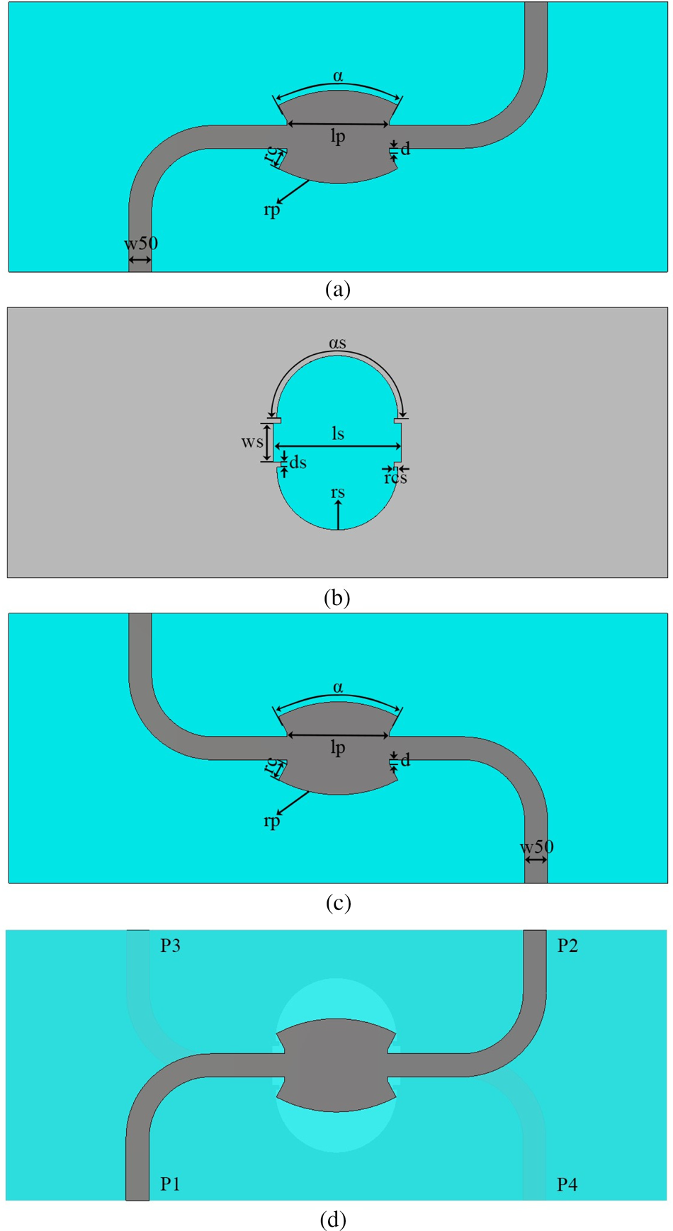
Fig. 1. (a) Front view of the top PCB card of the coupler. (b) Ground plane of both top and bottom PCB cards of the coupler. (c) Front view of the bottom PCB card of the coupler. (d) Transparent view of the coupler.
The electrical and physical properties of the PCB cards that are used in this multi-layer structure are εr = 3, tan δ = 0.017 and PCB cards thickness is 0.508 mm. In order to design a multi-layer aperture coupled coupler and acquire initial design dimensions for butterfly shaped resonators, the static approach mentioned in [Reference Wong, Hanna, Picon and Baudrand14] is utilized. In Fig. 2, the coupler model used for quasi-static analysis is presented. As can be seen from Fig. 2, the resonators and aperture in [Reference Wong, Hanna, Picon and Baudrand14] are both rectangularly shaped. Both resonators and aperture have the same length of L. In this study, to be able to acquire initial design parameters for butterfly shaped resonator, area equivalent rectangularly shaped resonators and aperture will be used. Quasi-static approach presented in [Reference Wong, Hanna, Picon and Baudrand14] combines relationship between coupling and characteristic impedance of the structure by utilizing from even and odd mode impedances:


where


Fig. 2. Coupler model used for quasi-static analysis in [Reference Wong, Hanna, Picon and Baudrand14].
The ratio K(k)/K′(k) in equations (1) and (2) are calculated by using Hilberg formulas [Reference Hilberg15] as follows:


However, in order to simplify the model and make it more realizable, upper and lower shields are removed from the model shown in Fig. 2 by modifying ho such that ho→∞. Hence equations (4) and (6) are equal to zero while new even and odd mode impedances are given in equations (9) and (10) as follows:


First of all, even and odd mode impedances (Zoe and Zoo) of equivalent rectangular structures are calculated using equations (9) and (10). In order to design a hybrid quadrature coupler, magnitude of the coupling between output ports should be 3 dB which means coupling coefficient C must be equal to 0.5. In equations (11) and (12), relationship between coupling coefficient C and even/odd mode impedances Zoe/Zoo are given:


Using equations (7) and (8), it has been found that Zoe = 120.9 Ω and Zoo = 20.7 Ω for Zo = 50 Ω for all input and output ports. Initially, length of the resonators lp and length of the aperture ls, is equal to each other as they are quarter of effective wavelength, λeff. Hence 90° phase difference will be acquired between output ports of the coupler. Using equation (9), initial lp and ls values are found to be 5.31 mm. Hence length of the rectangular resonators and aperture L is also equal to 5.31 mm:

In order to find width of the equivalent rectangular resonator W and width of the equivalent rectangular aperture G, equations (9) and (10) are solved by iterating ratios W/h and G/h for even and odd mode impedances that are calculated using equations (11) and (12). The dimensions of the W and G are found to be 4.47 and 4.74 mm, respectively. In order to find initial dimensions of resonators and aperture of the proposed design, it is assumed that area of butterfly shaped resonators and slots should be equal to their rectangularly projected counterparts. Areas (A) of the butterfly shaped resonators and slots are calculated as follows:

Parameter d in equation (14) is the distance between a wing of the butterfly shaped resonator to the 50-Ω transmission line. This distance d is inserted into the butterfly shape in order to make sure ease of production and it is set to 0.25 mm. When equation (14) is solved iteratively for rc and α, as an initial point radial edge of the resonator rc is found to be 0.9 mm while angle of the arc of the butterfly shaped resonator α is found to be 52.6°. Besides, butterfly cavity requires additional calculations in order to represent rectangular middle section which is slightly different than the resonator. Following the same methodology, using equation (14) where resonator dimensions are replaced with aperture dimensions, radial edge of the aperture rcs is found to be 0.2 mm and angle of the arc of the butterfly shaped aperture αs is found to be 135.9 mm. The remaining parameter ds which is the distance between radial edges and straight section of the shapes at aperture is also set to 0.25 mm same as parameter d. However, these results are not suitable to be able to operate with a wideband performance since static approach is only solved at the center frequency of operation. Therefore, using the initial values acquired by analytical methods, further electromagnetic simulations and optimizations are performed to get wideband performance.
Results and discussion
All simulations in this study are performed in the CST Microwave Studio environment. In Fig. 3, the optimal simulated s-parameters of the proposed quadrature hybrid coupler and previously calculated rectangularly shaped quadrature hybrid coupler are presented. It is seen from Fig. 3 that return loss of the hybrid coupler is below −18 dB within the whole frequency band while rectangularly shaped hybrid coupler reaches to as much as −12 dB along the whole frequency band. According to Fig. 3, isolation between input port and isolated port is <−18 dB for the proposed structure while rectangularly shaped hybrid coupler's isolation performance deteriorates up to −11 dB at the end of the frequency band. In terms of coupling, response of the proposed structure is better than the rectangularly shaped hybrid coupler. Coupling of the rectangularly shaped hybrid coupler deteriorates rapidly as operating frequency gets further away from center of the operating frequency band.

Fig. 3. Simulated s-parameters of the proposed quadrature hybrid coupler and rectangularly shaped quadrature hybrid coupler.
In this study, instead of combining PCB cards manually with a tape, it has been decided to combine them with a prepreg material during the production process. Prepreg materials are the main components that are used to manufacture multilayer PCB structures. They are manufactured in a controlled environment where fiber cloths are impregnated with resin materials so that their electrical and physical properties are more reliable compared to the tapes. They are not only used as a bonding material but also used as an insulating material between PCB cards. In our topology prepreg is used as a bonding material. During the manufacturing process it has been placed in between top and bottom PCB cards and all layers are merged under pressure and heat. There are three main advantages to using prepreg material instead of tapes. First one is that electrical properties of the prepreg materials are known and reliable. To be able to design a broadband microwave component with multi-layer stack-up, it is of paramount importance to model all substrate materials with correct electrical properties. The second advantage of prepreg materials is that alignment errors are minimized in a controlled manufacturing environment where automated optical inspection and metrology equipment are used during the production process. Final advantage is that thickness inhomogeneities are minimized due to the merging process which is performed under pressure and temperature. Compared to any manual bonding process, usage of prepreg materials to realize multi-layer PCB stack-up is more reliable, repeatable, and more stable.
As an internal bonding agent, 0.092 mm thick prepreg material with ɛr = 2.91 and tan δ = 0.0018 is inserted in between PCB cards. In Fig. 4 the PCB layout with and without prepreg material is indicated.

Fig. 4. (a) PCB stack-up without any bonding agent. (b) PCB stack-up with prepreg material.
In Fig. 5, s-parameters of the new design with prepreg material in between PCB cards is shown. It is seen from the results that there are undesired performance dips at several frequencies. Further look at to these dips yielded that although standing waves are formed on the prepreg material due to the gap between ground planes of the PCB cards.

Fig. 5. s-parameters of the simulated quadrature hybrid coupler with prepreg material in between PCB cards.
In Fig. 6 electric fields at a plane in between PCB cards when there is no bonding agent and prepreg material is given at 7.56 GHz where the first dip occurs. It is seen from Fig. 6 that there is a serious standing wave problem due to the unwanted surface waves on prepreg materials at frequencies where there are unwanted performance dips.

Fig. 6. (a) Electric field distribution at a plane in between PCB cards when there is no bonding agent. (b) Electric field distribution at a plane in between PCB cards when there is prepreg material in between PCB cards.
Further parametric study has been performed to understand the nature of this problem. First of all, gap between PCB cards has been increased to see when standing waves began to form. A parameter sweep study showing effects of gap between PCB cards on return loss is given in Fig. 7.

Fig. 7. Effect of gap between PCB cards on return loss.
It is seen from Fig. 7 that after gap becomes larger than 20μm standing waves began to form and degrade the performance of the coupler. Usually, to be able to realize such multilayer structure mechanically, the bonding agent in between PCB cards is used. Often the electrical properties of such an agent are not known and typically they have a minimum thickness of 0.1 mm. In order to understand the effect of εr of the bonding agent on the coupler performance, 0.1 mm thick material with tangent loss of 0.01 has been inserted in between PCB cards. Effects of change in εr of the bonding material on return loss and phase difference between output ports are given in Figs 8 and 9.

Fig. 8. Effect of change in εr of the bonding material on return loss.

Fig. 9. Effect of change in εr of the bonding material on phase difference between output ports.
It is seen from Fig. 8 that as εr increases, return loss of the coupler changes drastically. Furthermore, when Fig. 9 is examined, it is also seen that as εr increases, number of unwanted sudden phase dips increases.
Another issue about this multilayer aperture coupled structure is alignment of the PCB cards. Axial shift between PCB cards may influence the performance of the structure negatively especially in terms of phase. In order to examine this issue, a parametric study that employs the same amount of axial shift at both horizontal and vertical axes is performed. In this study, no bonding agent is inserted between PCB cards and no gap between PCB cards was defined. The effect of axial shift on phase error for phase difference between output ports of the coupler when there is no gap between PCB cards is given in Fig. 10.

Fig. 10. Effect of axial shift on phase error for phase difference between output ports of the coupler when there is no gap between PCB cards.
It is seen from Fig. 10 that phase error for phase difference between outputs ports of the coupler increases up to approximately 4° even for a small axial shift of 0.4 mm. This issue may lead to serious performance degradation if not handled with utmost caution. In studies performed by the authors [Reference Abbosh and Bialkowski11, Reference Ahmed, Sebak and Dedidni13], PCB cards are combined to each other manually by a tape. Therefore, to be able examine this issue more realistically, a 0.1 mm thick material with εr = 3 and tan δ = 0.01 has been inserted between PCB cards and the same axial shift study is repeated. In Figs 11 and 12 effect of change in axial shift on return loss and phase difference between output ports of the coupler are presented.

Fig. 11. Effect of change in axial shift on return loss.

Fig. 12. Effect of change in axial shift on phase difference between output ports of the coupler.
It is seen from Figs 11 and 12 that using a bonding agent between PCB cards without taking any precautions may result in serious performance loss. This issue can be clearly seen in [Reference Ahmed, Sebak and Dedidni13]. Most of the discrepancies between simulation and measurement results of [Reference Ahmed, Sebak and Dedidni13] can be attributed to the misalignment and formation of unwanted standing wave within the operating frequency band. However, this issue can be missed if there is not enough measurement points as in [Reference Abbosh and Bialkowski11].
So as to fix this problem and avoid unwanted electric fields on the surface of the PCB cards, it has been decided to cage these electric fields around the microstrip lines with vias. To be able to effectively shield electric fields, vias' lengths have been chosen such that vias connect top layer conductor of the upper PCB card to bottom layer conductor of the lower PCB. In other words, through hole plated vias have been inserted to the structure. In order to avoid an unwanted surface waves on the prepreg material, not only the length of the vias but also placement of the vias on PCB cards have a significance. Therefore, although inserting shielding vias, distance between vias to the microstrip lines have been chosen carefully by using simulations so that inserted vias do not affect existing electric field distribution of the microstrip line. This resulted in coplanar waveguide (CPW) like structure. Generally, side metallic surfaces in CPW are much closer to the transmission lines. However, in this study, in order not to effect characteristics impedance of the transmission lines, gaps between transmission lines and metallic side surfaces are kept such that CPW's transmission line impedances are approximately the same as microstrip transmission line. Geometry of the new model with vias is given in Fig. 13.

Fig. 13. (a) Front view of the top PCB card of the proposed quadrature hybrid coupler. (b) Ground plane of both top and bottom PCB cards of the proposed quadrature hybrid coupler. (c) Front view of the bottom PCB card of the proposed quadrature hybrid coupler.
In Fig. 14, electric field distribution at a plane in between PCB cards after the insertion of shielding vias is given. It is seen from Fig. 14 that insertion of vias prevent standing waves on prepreg material.

Fig. 14. Electric field distribution at a plane in between PCB cards after the insertion of shielding vias.
After insertion of vias, further optimization is performed on the structure to acquire better results. Optimal dimension values are given in Table 1.
Table 1. Dimensions of the designed quadrature hybrid coupler

In order to see how robust this design is in terms of vulnerability to prepreg height and misalignment between PCB cards some parametric studies have been performed. The effect of change in height of prepreg material while shielding vias are present on return loss and phase difference between output ports of the coupler is given in Figs 15 and 16.

Fig. 15. Effect of change in height of prepreg material while shielding vias are present on return loss.

Fig. 16. Effect of change in height of prepreg material while shielding vias are present on phase difference between output ports of the coupler.
It is seen from Fig. 15 that change in height of the prepreg material has a minimal impact on return loss of the coupler. Minimum return loss value of the coupler even with 0.4 mm thick prepreg material is better than −18 dB and no unwanted standing waves are present.
When the effect of change in thickness of the prepreg material on coupler in terms of phase difference is examined, it is <1.5°. Looking at Figs 15 and 16, it can be said that the formation of standing waves can be prevented by the proposed model. To be able to judge the proposed model in terms of misalignment, similar axial shift study has been carried out as previous models. In Fig. 17, the effect of axial shift on phase error for phase difference between output ports of the coupler when prepreg material and shielding vias are present, is given.

Fig. 17. Effect of axial shift on phase error for phase difference between output ports of the coupler when there is prepreg material and shielding vias are present.
The shielding vias that are inserted into the model are 0.2 mm away from the edge of the ground plane. Therefore, misalignment above 0.2 mm is not possible due to the optical inspections and metrology equipment that are used during the production process. It is seen from Fig. 17 that the maximum phase error that can be seen due to the misalignment is <1.1° with the proposed topology. These results are even better that the results indicated in Fig. 10 and the proposed structure not only solves the issue of the formation of standing waves but also decreases vulnerabilities against height of bonding agent and misalignment between PCB cards.
The geometry of the manufactured quadrature hybrid coupler is shown in Fig. 18. The size of the manufactured design is 35 mm × 17 mm. Port numbers for the measurement results are marked on the manufactured geometry as shown in Fig. 18. In order to measure the whole performance of the coupler, a two-port PNA network analyzer is utilized. Connectors that are not used during two port measurements are terminated with 50-Ω terminators.
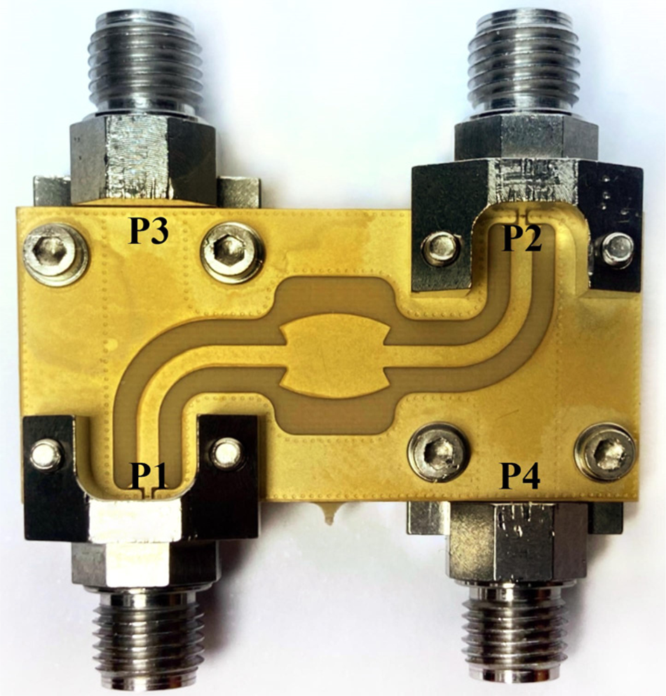
Fig. 18. Geometry of the manufactured quadrature hybrid coupler.
Figure 19 shows the s-parameter results of the simulated and measured quadrature hybrid couplers. It is seen from Fig. 19 that measured return loss and isolation results agree well with each other.

Fig. 19. s-parameter results of the simulated and measured quadrature hybrid coupler.
In Fig. 20, simulated and measured amplitude imbalances between the output ports of the directional quadrature hybrid coupler are shown. Along most of the frequency band measured and simulated amplitude imbalances seem to be very consistent with each other. It is seen that difference between measured and simulated amplitude imbalances is <0.2 dB within the whole frequency range.

Fig. 20. Simulated and measured amplitude imbalance between output ports.
Figure 21 indicates simulated and measured phase difference results between output ports. It is seen from Fig. 21 that the manufactured quadrature hybrid coupler has also good results in terms of phase response. The phase imbalance of the manufacture structure is <±2.5° within 3–12 GHz. It is seen that difference between the measured and simulated phase imbalance is <1.3° within the whole frequency range.

Fig. 21. Simulated and measured phase difference between output ports.
The performance of the quadrature hybrid couplers that are mentioned in the literature and proposed design are presented in Table 2. When performance of all structures in Table 2 is compared in terms of operating bandwidth, the proposed structure seems to have the widest frequency bandwidth by far except [Reference Abbosh and Bialkowski11, Reference Ahmed, Sebak and Dedidni13]. Although some of the papers did not include any phase imbalance data of the manufactured designs, it is safe to say that the proposed design has the lowest phase imbalance within the widest frequency range compared to other studies. In addition to that, in terms of sizes mentioned in Table 2, the proposed design is fairly compact considering its operating frequency band.
Table 2. Performance comparison of phase shifters operating at Ka-band in the literature and proposed phase shifters

Conclusion
In this paper, a multi-layer quadrature hybrid coupler that can operate within 3–12 GHz is designed. Multilayer stack-up of the proposed quadrature hybrid coupler is realized by combining top and bottom PCB cards with a prepreg material in order to obtain high precision alignment in manufacturing. However, prepreg material caused unwanted surface waves which resulted in undesired performance dips at several frequencies. In order to avoid unwanted effects of using a prepreg material in between top and bottom PCB cards, shielding vias around resonators and microstrip lines is utilized. The proposed design is both compact and has widest frequency bandwidth compared to other topologies mentioned in previous studies. When measurement results of the proposed design are evaluated, it can be said that the proposed structure not only has minimal amplitude imbalance between its output ports but also has minimal phase error of ±2.5° along the whole operating band.
 Meliksah Yayan received a degree in electrical and electronics engineering from the Bilkent University in 2009 and received his M.S. degree in electrical and electronics engineering 2012. He now works as an electromagnetic design engineer at Aselsan Ind. Inc. His main research interests are design and optimization of antennas and microwave devices.
 Alparslan Cagri Yapici received his B.Sc. degree in electrical and electronics engineering from the Hacettepe University, Ankara, in 2001, his M.Sc. degree in electrical and electronics engineering from the Middle East Technical University, Ankara, Turkey, in 2004, and his Ph.D. degree in electronics engineering at Erciyes University, Kayseri, Turkey, in 2008. He is now working as an Assistant Professor at Baskent University, Ankara, Turkey. His current research interests are in the areas of RF circuit design, RF power amplifier linearization for wireless communication systems, and Antenna design and optimization.


