


Introduction
Ultra-wideband (UWB) communication has become attractive since the Federal Communications Commission (FCC) released the frequency band of 3.1–10.6 GHz [1]. In a UWB system, compact and low-cost antenna design has always been a key issue. The monopole antenna can be applied in many areas, such as short-range technology for wireless communication, wireless body area network, UWB radar, and imaging systems with superior penetration and high resolution. Many novel UWB antenna designs have been proposed, where small printed monopole antennas with different slots and backplanes have drawn special attention because of their compactness and simple structure [Reference Ojaroudi and Ojaroudi2–Reference Ojaroudi, Yazdanifard, Ojaroudi and Naser-Moghaddasi6]. In [Reference Ojaroudi, Yazdanifard, Ojaroudi and Naser-Moghaddasi6], the impedance bandwidth has been successfully increased by cutting an inverted T-shaped slot on the radiating patch and adding an inverted T-shaped conductor to the ground plane. Furthermore, UWB antennas with one [Reference Young-Jun, Ki-Hak, Dong, Seung-Sik and Seong-Ook7–Reference Sharma, Vyas and Yadav11] or more band-notches [Reference Shinde and Mishra12–Reference Sarkar, Srivastava and Saurav20] are proposed to avoid unexpected interferences with other existing wireless communication systems such as the WLAN operating in 5.15–5.35 and 5.725–5.825, and the WiMAX in 3.3–3.7. Changing the current flow on the radiating patch of the antenna with a narrow slot is one of the easy and commonly used technique to reject a fixed frequency band [Reference Young-Jun, Ki-Hak, Dong, Seung-Sik and Seong-Ook7, Reference Chang and Kang10].
Most recently, reconfigurable antennas have also been proposed to avoid the frequency interference [Reference Nikolaou, Kingsley, Ponchak, Papapolymerou and Tentzeris21–Reference Tang, Wang, Deng and Ziolkowski23]. With the reconfigurable structures providing switchable band-notches, the antenna can be operated throughout the UWB spectrum whenever there is no coexisting system while filtering out interferences when necessary. In [Reference Nikolaou, Kingsley, Ponchak, Papapolymerou and Tentzeris21], microelectromechanical system switches are integrated to the antenna structures to switch the notching of the WLAN band, whereas in [Reference Valizade, Ghobadi, Nourinia and Ojaroudi22] a PIN diode is added to bridge one of the antenna slots to switch the band-notched function in the range of 5–6 GHz. Recently, Tang et al. [Reference Tang, Wang, Deng and Ziolkowski23] proposed a planar UWB antenna with continuously tunable, independent band-notches for cognitive radio applications. Band-notched frequency below 5 GHz and above 5 GHz is realized by adding varactor diode between the rectangular strip on the top and the leg of the parasitic element on the bottom.
In [Reference Sharma, Vyas and Yadav11], a UWB antenna with the tunable notched band is designed. The bandwidth of the notched band can be tuned by changing the air-gap distance between two T-shaped strips placed inside the radiating annular patch. Inspired by the document [Reference Sharma, Vyas and Yadav11], a compact reconfigurable UWB antenna design is proposed with dual switchable band-notches covering the 4.9–6.3 GHz band and the 3–3.8 GHz band to overcome the problem of unwanted interference from existing WLAN and WiMAX environment. The proposed antenna has advantages in frequency selection for different interference environment. The band-notching function is realized by electromagnetically adjusting the coupling between two pairs of T-shaped strips protruded inside the radiation patch through five PIN diodes. In other design, only two status can be realized by controlling the switch [Reference Nikolaou, Kingsley, Ponchak, Papapolymerou and Tentzeris21–Reference Tang, Wang, Deng and Ziolkowski23], and in our design, three status at UWB, WiMAX, or WLAN bands can be realized by changing the status of the diodes and reconfigure the antenna into three different structures. The proposed antenna is simulated, manufactured, and tested. Good agreements between simulation and measurement verify the design concept.
Antenna design
The proposed reconfigurable UWB antenna is printed on an FR4 substrate with a thickness of 1.5 mm. The relative permittivity of the substrate is ε r = 4.3, and loss tangent is 0.018. Figure 1 shows the schematics of the top and bottom layers of the antenna conductors. The basic antenna structure consists of a circular radiating patch with a radius R = 10 mm. A cambered conductor is placed at the bottom of the substrate serving as a ground plane. The proposed antenna is fed by a 50 Ω transmission line connected to a 50 Ω SMA connector. As illustrated in Fig. 1, two pairs of T-shaped strips are protruded inside the radiation patch working as half-wave resonant structures which perturb the resonant response [Reference Ojaroudi and Ojaroudi13].
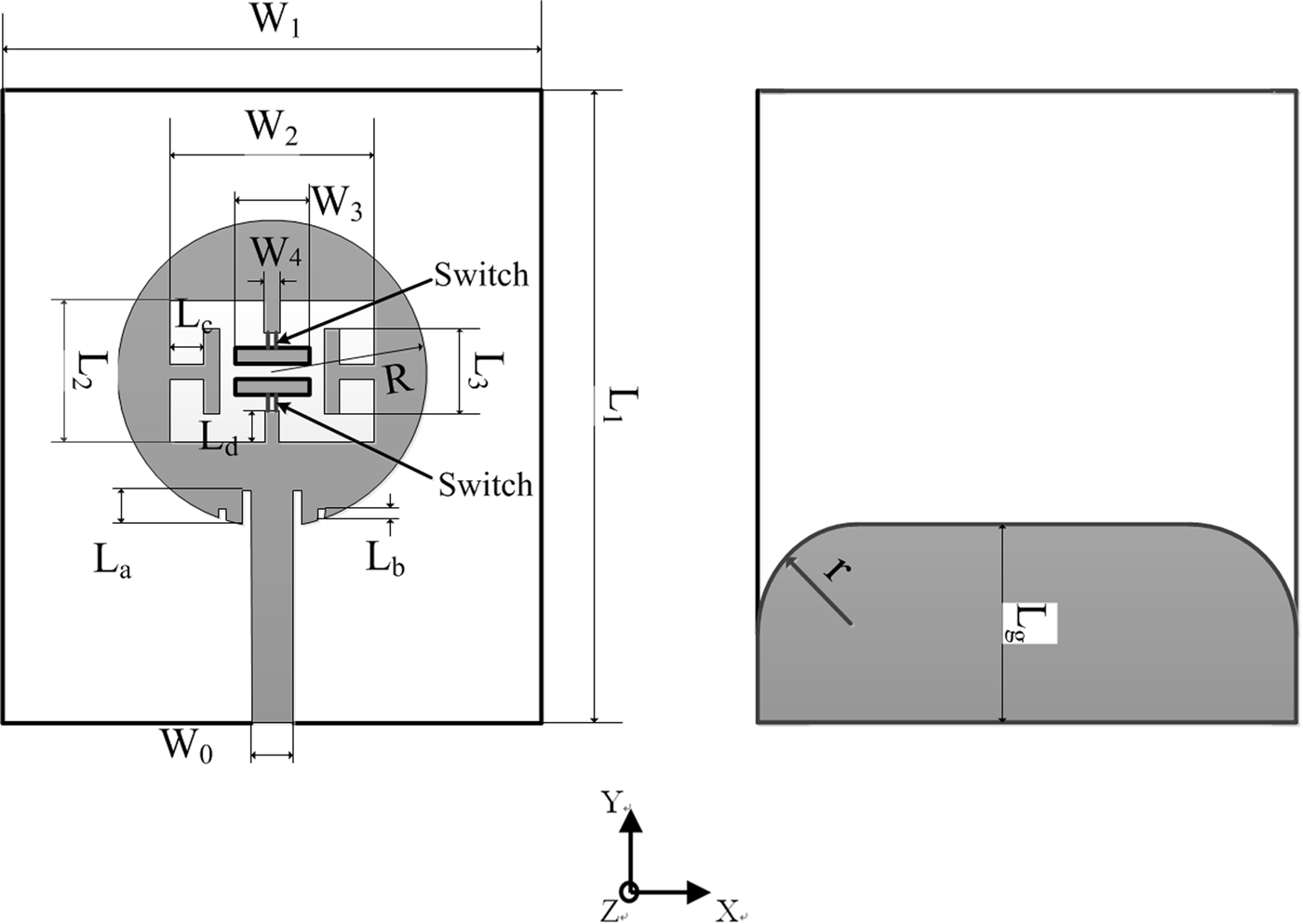
Fig. 1. Schematic representations of the proposed reconfigurable UWB antenna: (a) top layer; (b) bottom layer.
The evolution of the proposed slot antenna is shown in Fig. 2, and the corresponding reflection coefficient curves are compared in Fig. 3. As shown in Fig. 2(a), a printed circular disk monopole antenna with the rectangular ground (type-A) is presented. This type-A antenna has wide impedance bandwidth. The corresponding reflection coefficient curve of type-A antenna is shown in Fig. 3. However, the bandwidth of type-A antenna is 2.7–7.5 GHz, which does not meet the requirements of UWB 3.1–10.6 GHz. Figure 2(b) shows type-B antenna with the modified ground plane. It is found that the impedance at high frequencies has been improved by designing the ground plane with two circular tangent angles, as shown in Fig. 3. As we can see from Fig. 3, the corresponding reflection coefficient of type-B is near the −11 dB, which is not very good. To further improve the impedance characteristics in the antenna band, two pairs of narrow slots near the feeding line are added, as shown in Fig. 2(c). As seen in Fig. 3, the reflection coefficient curve is further reduced after adding the narrow slots on the radiating path, since the increased narrow slots on the radiation patch can extend the current path on the radiation patch, and improve the impedance characteristics in the band. Compared with type-A antenna, the bandwidth of type-C antenna is improved both at low and high frequencies and meeting the requirements of UWB. The type-C antenna can be further improved in terms of reconfigurability. For this purpose, two pairs of T-shaped strips are designed inside the circular radiation patch, leading to the type-D design as shown in Fig. 2(d). Type-D is one configuration of the proposed antenna functioning as UWB antenna with 3.5 GHz band-notched function. In addition, five PIN diodes are added to short or open the antenna slots among the T-shapes. The antenna can be reconfigured to different structures by controlling the status of the diodes. Three possible connections are shown in Fig. 4, corresponding to the antenna functionalities as (a) UWB antenna, (b) UWB antenna with a band-notch centered at 3.5 GHz, and (c) UWB antenna with a band-notch centered at 5.5 GHz. Simulated return losses of the three configurations are shown in Fig. 5. In order to isolate the RF signal from the DC biasing voltage, a 100 pF DC blocking capacitor was used between the PIN diodes and the antenna metal patch, as shown in Fig. 4. This way RF and DC isolation was completed in the circuit. HPND-4005 PIN diode model was selected, which is designed for use in stripline or microstrip circuits. The extremely low capacitance of the HPND-4005 makes it ideal for circuits requiring high isolation in a series diode configuration. Forward biasing the diode through a DC forward voltage (V F) of 1 V can be seen as an equivalent circuit of a series combination of inductance (L s = 0.15 nH) and resistance (R s = 4.7 Ω), and when the PIN diode is off, there is one resistance of 5 kΩ parallel with a capacitance of 0.017 pF as shown in Fig. 6(a). An RF choke (L c) of 0.15 nH in series with the diode efficiently implements RF isolation in the circuit. Three configurations of the proposed antenna functioning as (a) UWB antenna, (b) UWB antenna with 3.5 GHz band-notch, and (c) UWB antenna with 5.5 GHz band-notch curves of the simulated S 11 of the ideal switch and the equivalent circuit of PIN diode are compared, as shown in Fig. 6. It can be seen from Fig. 6 that although the impedance matching bandwidth of the diode is narrower than the ideal switch at high frequencies, the performance at low frequencies is excellent and has little effect on the other performance of the antenna. The antenna is simulated and optimized using CST MICROWAVE STUDIO [htttp://www.cst.com] targeting the best UWB performance and the two notched bands. The optimal antenna is manufactured with the following dimensions: W 0 = 2.84 mm, W 1 = 35 mm, W 2 = 13.2 mm, L 2 = 9 mm, W 3 = 4.8 mm, L 3 = 5.5 mm, W 4 = 1 mm, L a = 2.22 mm, L b = 0.75 mm, L c = 2.2 mm, L d = 2 mm, R = 10 mm, r = 7 mm.
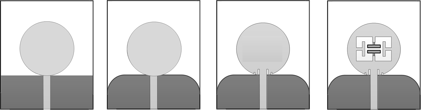
Fig. 2. The evolution of the proposed slot antenna, (a) type-A, (b) type-B, (c) type-C, (d) type-D.
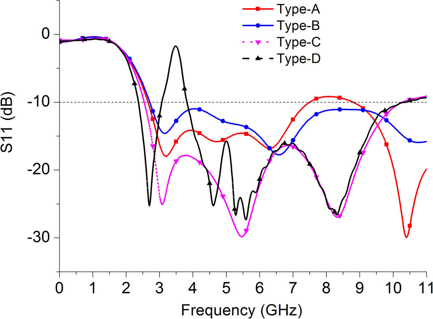
Fig. 3. Comparison of simulated reflection coefficients of the proposed antenna in Fig. 2.

Fig. 4. Three configurations of the proposed antenna functioning as (a) UWB antenna, (b) UWB antenna with 3.5 GHz band-notch, and (c) UWB antenna with 5.5 GHz band-notch.
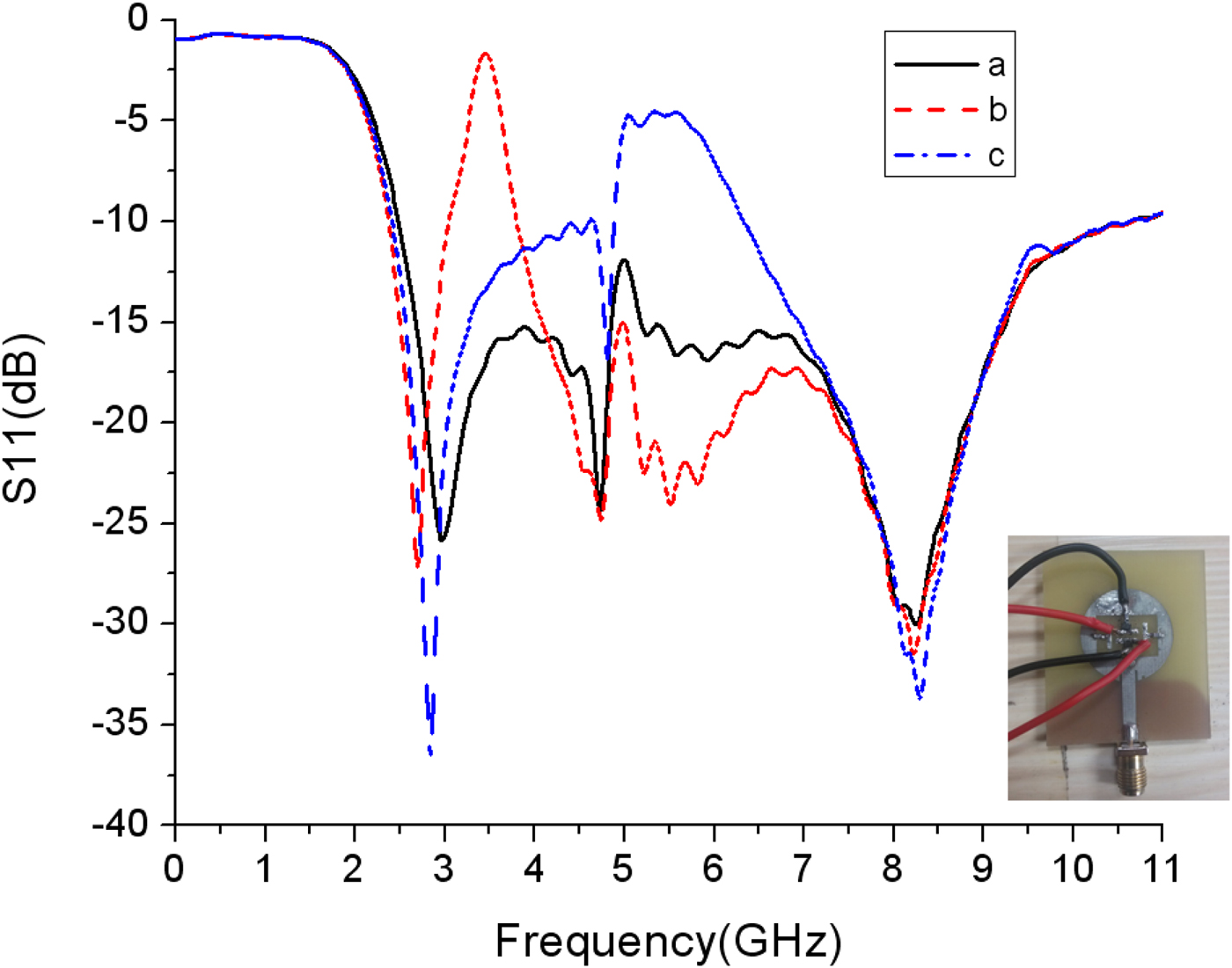
Fig. 5. Simulated return losses of the three configurations: (a) UWB, (b) UWB with 3.5 GHz notched band, and (c) UWB with 5.5 GHz notched band.
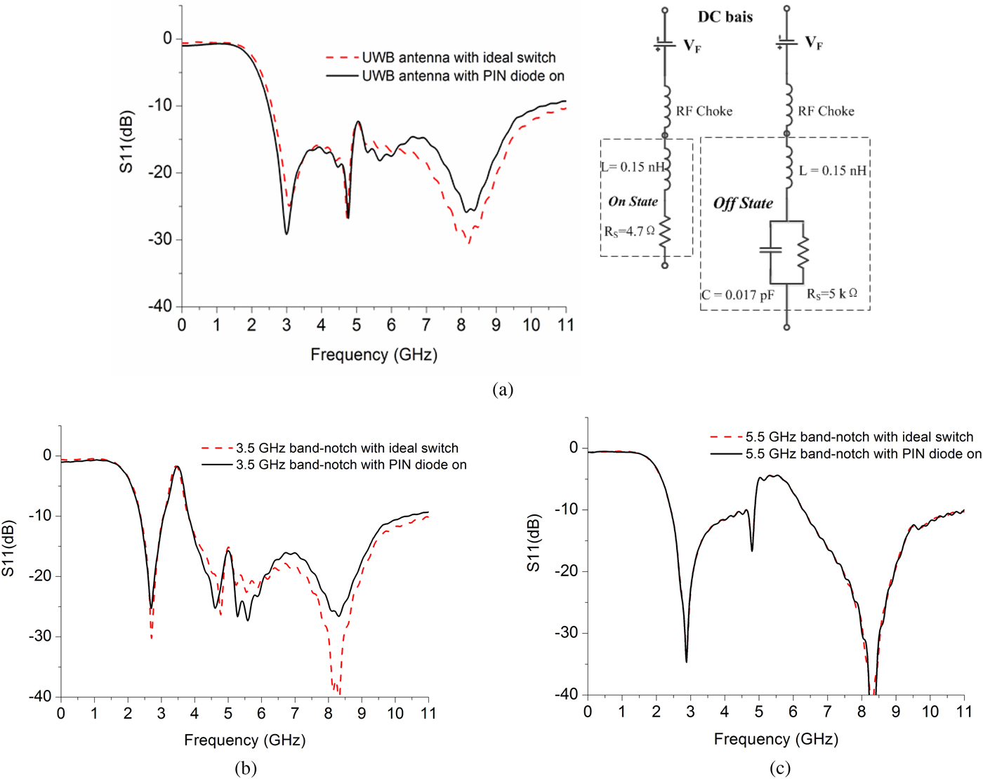
Fig. 6. The equivalent circuit of the PIN diode with the comparison between the S 11 curves of three configurations of the proposed antenna: (a) UWB, (b) UWB with 3.5 GHz notched band, and (c) UWB with 5.5 GHz notched band.
Results and discussions
The proposed antenna is manufactured and tested. In this section, the numerical and experimental results of the proposed reconfigurable antenna are presented and discussed, including its frequency- and time-domain analysis.
Frequency-domain analysis
Figure 5 shows the simulated return loss for the three configurations shown in Fig. 4. Very good UWB performances, as well as the two expected notched bands, are observed. Therefore, we could conclude that the band-notch characteristics are significantly affected by the connections of the two pairs of T-shaped strips due to the change in surface current path. In order to better understand the occurrences of band-notches, we simulated the current distributions at the two notched frequencies of 3.5 and 5.5 GHz as shown in Fig. 7. It is found that the dense current distributions around the T-shaped strips protrude inside the circular radiating patch. At the notch frequencies, the current concentration on the edges of the square ring and the feeding stripe produces the desired high attenuation [Reference Ojaroudi, Yazdanifard, Ojaroudi and Sadeghzadeh9]. At 3.5 GHz, the maximum current density occurs at the T-strips inside the patch ring, while at 5.5 GHz, it appears at the edges of the horizontal T-strips protrude inside the circular radiating patch and the narrow slots near the feeding line.
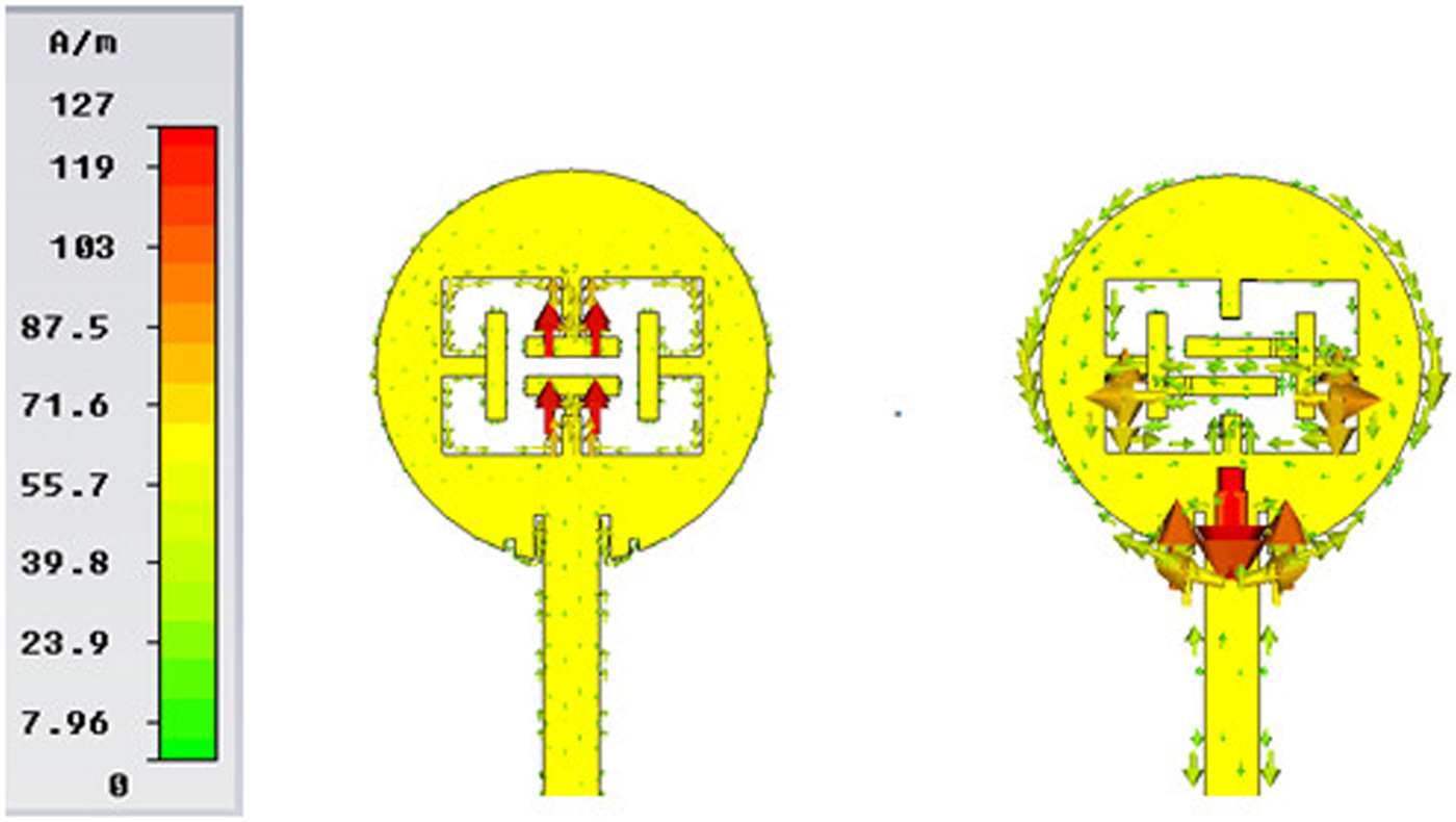
Fig. 7. Simulated current distributions at (a) 3.5 GHz and (b) 5.5 GHz.
Figure 8 shows comparisons between simulated and measured return losses for the three configurations. The overall agreement is good despite some small discrepancies possibly due to inaccuracy in the antenna parameters such as the fabrication dimensions, the thickness, and dielectric constant of the substrate, as well as the effect of the PIN diodes and their biasing circuit.
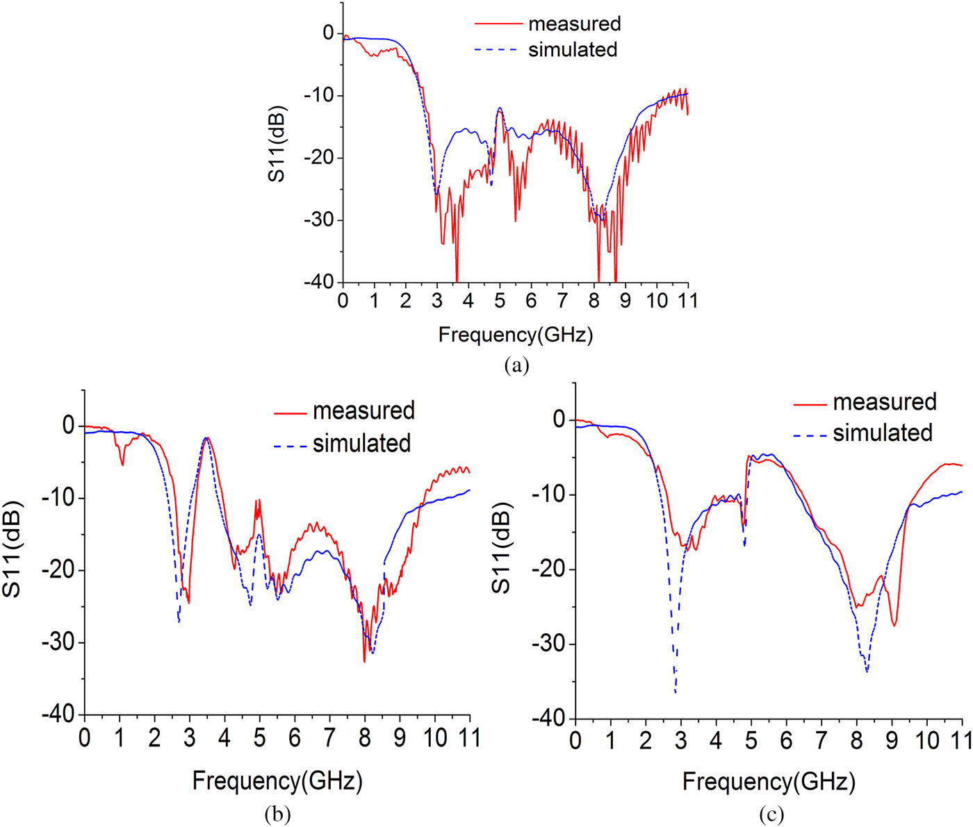
Fig. 8. Measured and simulated return loss for the three configurations of the proposed antenna: (a) UWB, (b) UWB with 3.5 GHz notched band, and (c) UWB with 5.5 GHz notched band.
Figure 9 shows the measured and simulated radiation patterns of the proposed UWB antenna at 4, 7, and 10 GHz, respectively. Good agreements are found in both the y-z plane (E-plane) and x-z plane (H-plane) results. The discrepancy is partly due to the pin diodes and the connected control lines during the measurement, whereas excluded in the simulation model. An acceptable approximate omnidirectional radiation pattern is observed which meets the requirement for UWB systems to be able to receive signals from all directions. The measured gains and efficiencies of the proposed antenna with and without band-notch are plotted in Fig. 10. Sharp decreases of antenna gains and efficiencies in the desired notched frequency band at 3.5 and 5.5 GHz are obtained. The measured gains and radiation efficiency is around 2.5 dBi and 80%, respectively. The proposed antenna is fully verified for rejecting interference signals from the WiMAX and WLAN systems.
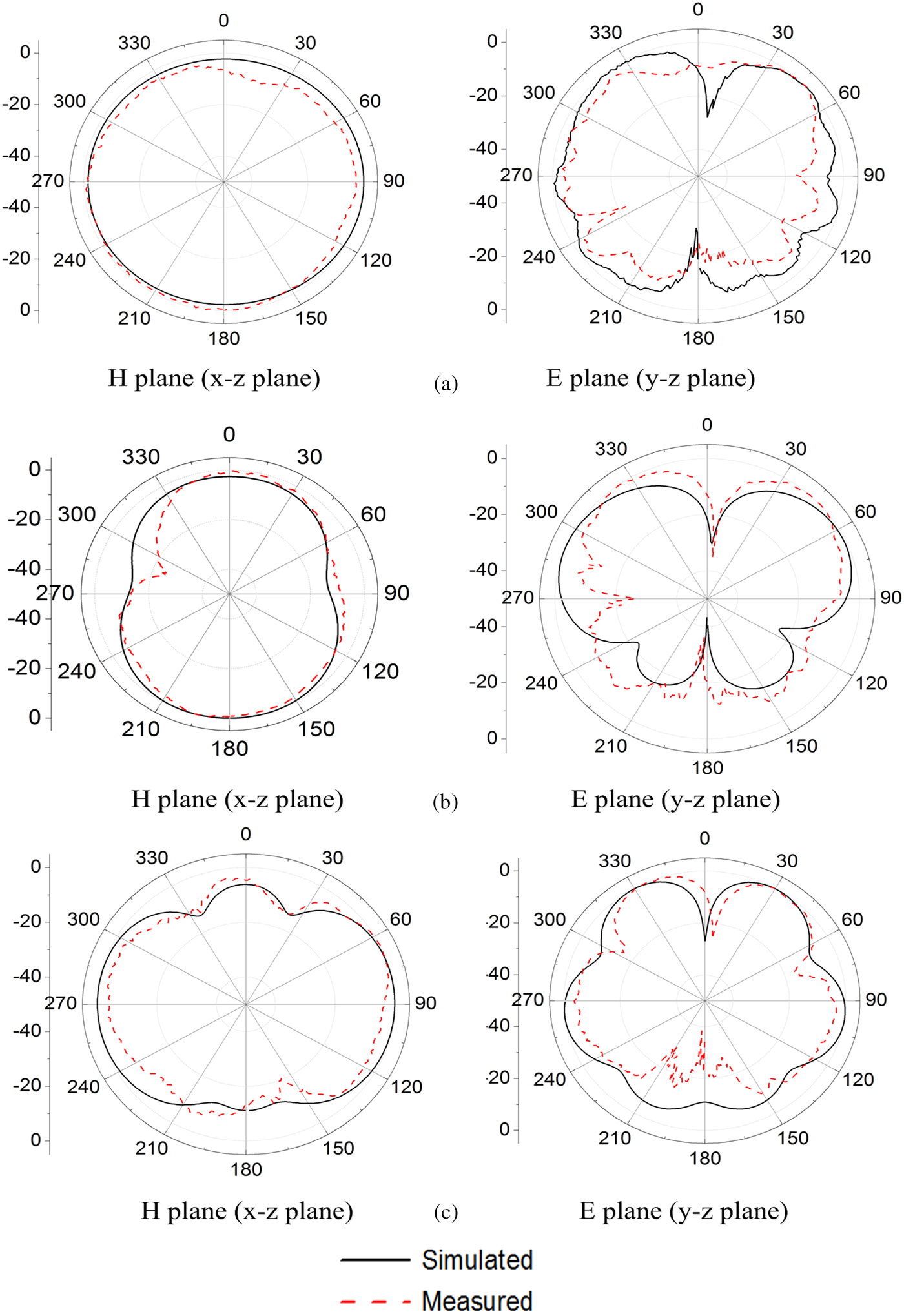
Fig. 9. Measured and simulated radiation patterns: (a) 4 GHz, (b) 7 GHz, (c) 10 GHz.
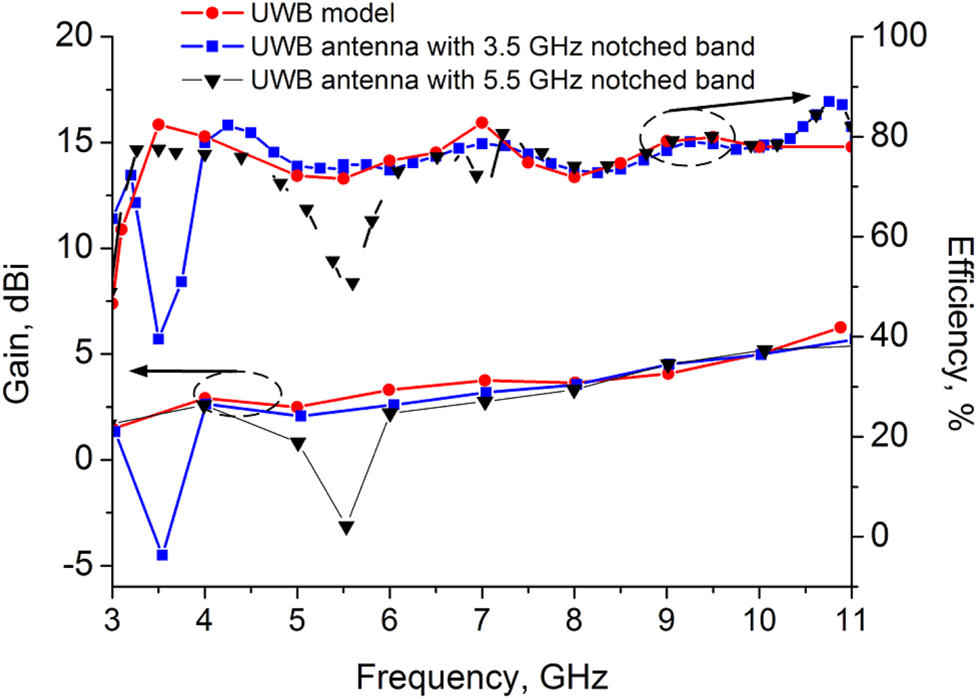
Fig. 10. Measured gains and efficiencies for three configurations of the proposed antenna.
Time-domain analysis
Having a good time-domain performance throughout the UWB band is another desired feature for a UWB antenna, dissatisfying that may lead to strong dispersion resulting in pulse distortion. To explore the time-domain characteristics of the proposed antenna, two identical antennas are employed as transmitter and receiver. The group delay is an important parameter in UWB antenna performance. It indicates the quantity of the far-field linearity. To measure it, two identical prototypes are used as transmitter and receiver, which are kept at a distance of 40 cm and placed in face-to-face and side-by-side orientations. Figure 11 shows the simulated group delay of the proposed antenna. As can be seen here, the group delay of the two antennas at 40 cm is stable at 1.5 ns, the variation of the group delay is kept small (within ± 0.5 ns) in the entire UWB band, except in the notched band.
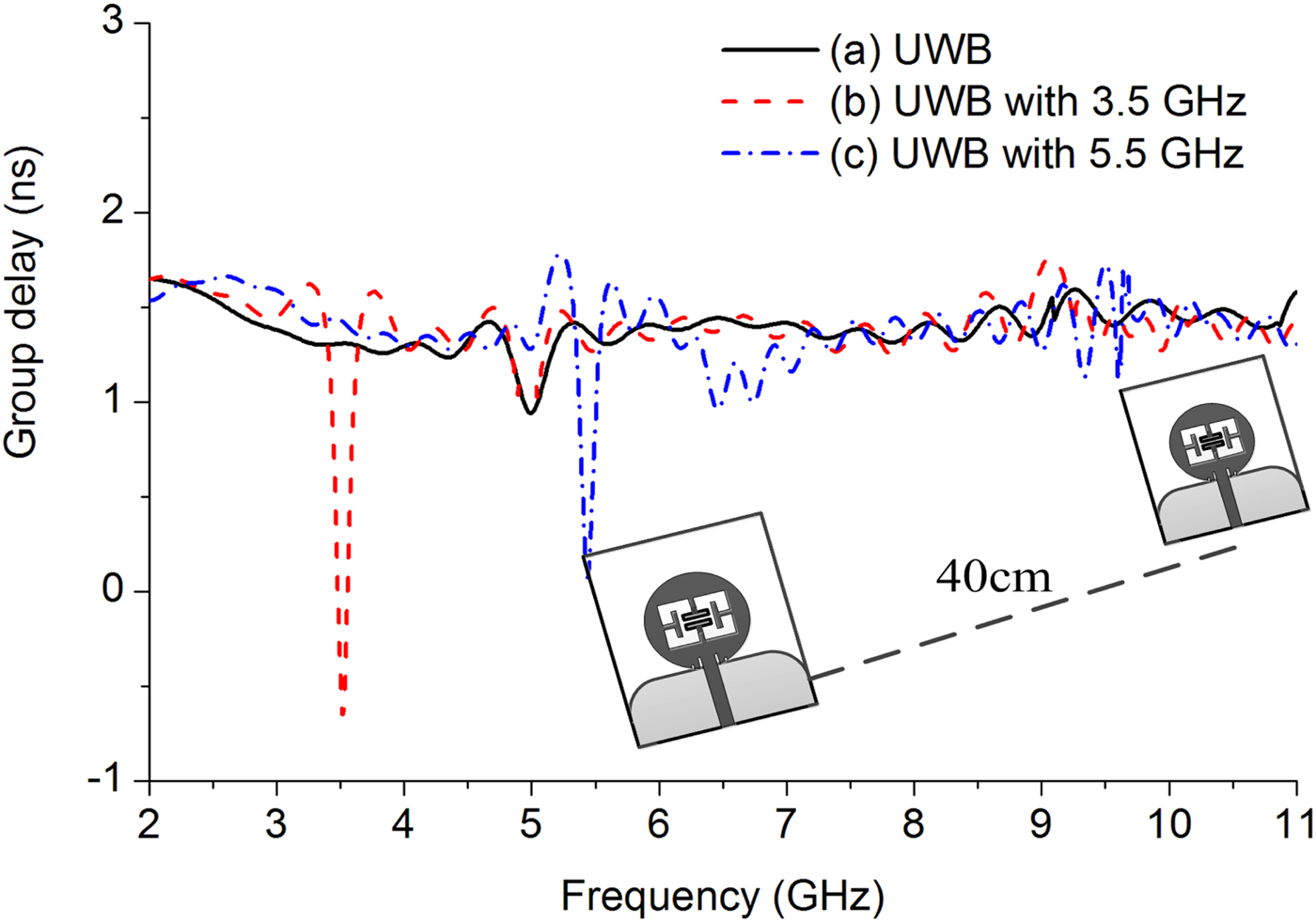
Fig. 11. Group delay of the three configurations for the proposed antenna.
To reduce the signal distortion caused by signal bandwidth and impedance mismatch, the short pulse reported in [Reference Telzhensky and Leviatan24, Reference Kim, Park and Joo25] is used to excite the UWB antenna. This signal is a fifth-order derivative of the Gaussian pulse and is given by
 $$\eqalign{ s_1(t) & = GM_5(t) = C\left( { - \displaystyle{{t^5} \over {\sqrt {2\pi} \sigma ^{11}}} + \displaystyle{{10t^3} \over {\sqrt {2\pi} \sigma ^9}} - \displaystyle{{15t} \over {\sqrt {2\pi} \sigma ^7}}} \right) \cr & \quad \times \exp \left( { - \displaystyle{{t^2} \over {2\sigma ^2}}} \right),} $$
where, σ = 51 ps, C is the amplitude parameter that can be used to comply with peak power spectral that FCC permits. The time-domain diagram of the pulse signal is show in Fig. 12. All the excitation signals used in the time-domain analysis of UWB antennas are this short pulse.
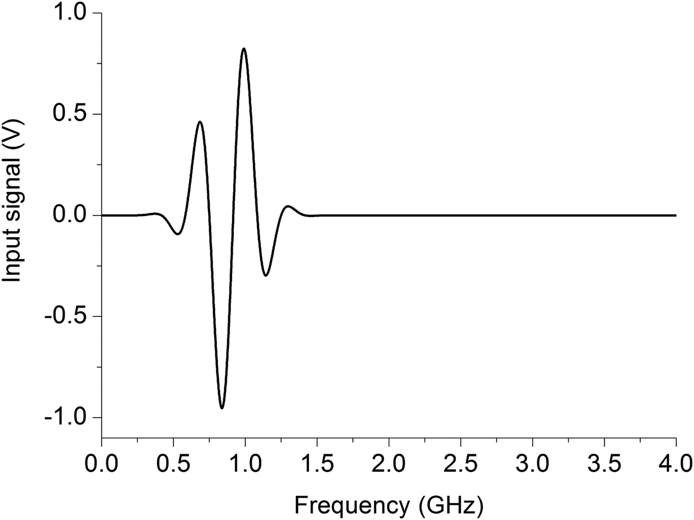
Fig. 12. A fifth-order derivative of the Gaussian input pulse.
To better analyze the time-domain characteristics of the antenna, each configuration of the proposed antenna is studied in two cases, which are face-to-face, side-to side, back-to-back. The received signals of the three configuration antennas in different cases are shown in Fig. 13.
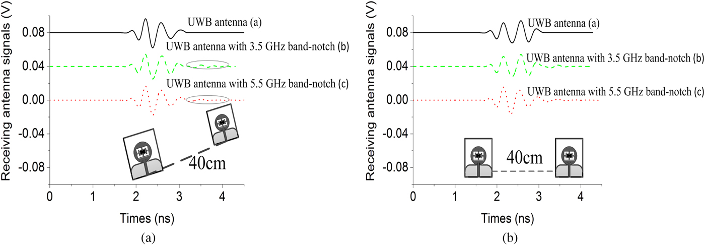
Fig. 13. Time-domain characteristics of UWB antenna in three configurations, (a) face-to-face, (b) side-to-side.
It can be seen that the UWB antenna with the notched function will introduce ringing distortion in both the cases face-to-face and side-to-side display, but the UWB antenna without notched band will not. This is mainly due to the impedance mismatch of the antenna in the notch band.
In addition, the antenna received signal amplitude and waveform in the side-to-side and face-to-face are relatively close. It can be seen that the antenna performs well in the time domain and has the better adaptability to meet the application of UWB.
In order to evaluate the time-domain characteristics of the UWB antenna, the correlation coefficients ρ is given as follows:
 $$\rho = \mathop {\max} \limits_\tau \left\{ {\displaystyle{{\int {s_1(t)s_2\left( {t - \tau} \right)dt}} \over {\int {s_1^2 (t)dt\sqrt {\int {s_2^2 (t)dt}}}}}} \right\},$$
where τ is a delay, which is varied to make numerator in (2) a maximum; S 2 (t) is the received pulse; S 1 (t) is the input pulse. Using (2), the fidelity factor of three configurations in Fig. 4 is calculated when the antennas were placed face-to-face and side-to-side condition. The calculated correlation factors of three configurations in different cases are compared in Table 1. It can be observed that both the face-to-face and side-to-side received signals of the three configurations are very similar to the input signal, and the correlation factor of the UWB antenna is bigger than the UWB antenna with the notched band. It is because the impedance mismatching at the notched band will introduce ringing distortion.
Table 1. The calculated correlation factors of three configurations in different cases

Conclusion
In this paper, a novel design of reconfigurable UWB-slot antenna with switchable dual band-notch function is proposed. By inserting two pairs of T-shape strips inside the radiation patch, while bridging or opening the slots via five PIN diodes, the proposed UWB antenna can be configured into a normal one operating throughout the entire UWB band, or one with band-notch at WLAN or WiMAX band which filtering away unwanted interferences intrinsically. The proposed antenna has a simple structure easy to fabricate. The measured results agree well with simulation. Good frequency- and time-domain performance confirm the proposed antenna being a good candidate for UWB applications.
Acknowledgements
This work was partly supported by the Key research and development plan of Shaanxi Province (2017ZDXM-GY-117), Xi'an Science and Technology Plan Project (2017080CG/RC043(XALG014)), (2017080CG/RC043(XALG013)), (2017080CG/RC043(XALG032)).
 Hailong Yang received the B.S. in communicating engineering from Heze University, Heze, China, in 2012. He received the M.S. degree in communicating engineering from Xi'an University of Technology, Xi'an, China, in 2015. He is currently working toward the Ph.D. degree at Xi'an University of Technology, Xi'an, China. His recent research interests include ultra-wideband antennas, reconfigurable antennas, and ultra-wideband filters.
 Xiaoli Xi (M'2010) received the B.S. degree in applied physics from the University of Defense Technology, ChangSha, China, in 1990; M.S. degree in biomedical engineering from Fourth Military Medical University, Xi'an, China, in 1998; and Ph.D. degree in electrical engineering from Xi'an Jiaotong University, Xi'an, China, in 2004. She is currently a Professor at the Department of Electric Engineering, Xi'an University of Technology, Xi'an, China. Her recent research interests include wave propagation, antenna design, and communication signal processing.
 Hualong Hou received the B.S. in communicating engineering from Xi'an University of Technology, Xi'an, China, in 2012. He is now a master degree candidate in electrical engineering at Xi'an University of Technology, Xi'an, China. His research interests include linear and non-linear CAD techniques and low-noise receivers.
 Yuchen Zhao received the B.S., M.S., and Ph.D. degrees in electronic science and technology from Northwestern Polytechnical University, Xi'an, China, in 2007, 2010, and 2014, respectively. He joined the faculty of Electronic Engineering Department, Xi'an University of Technology, Xi'an, China, in 2014. His research interests include wave propagation and effective medium theories.
 Yanning Yuan received the B.S. degree in electronic information from Liaoning Shihua University, FuShun, China, in 2004; and M.S. degree in communicating engineering from Xi'an University of Technology, Xi'an, China, in 2007. She joined the Shaanxi Lingyun Science and Technology Co., Ltd. and served as a project manager subsequently. She is currently a full-time research worker of Xi'an University of Technology, Xi'an, China. Her research interests include ultra-wideband antennas, multi-frequency antenna, and RF circuit.


