Introduction
Research on design and development of passive ultra-wideband (UWB) components has taken an exponential leap since the allocation of 3.1–10.6 GHz spectrum by the Federal Communications Commission (FCC) for indoor communications [1]. One such essential component of UWB systems is an UWB bandpass filter (BPF), which was designed using different principles [Reference Saito, Harada and Nishikata2–Reference Ghazali and Singh8]. An initial filter designed in this respect consisted of a microstrip line mounted on a composite lossy substrate to realize attenuation at high frequencies [Reference Saito, Harada and Nishikata2], whereas the basic idea of cascading high pass filters with low pass filters to develop an UWB-BPF was used in [Reference Tang and Chen3]. Perhaps, the most convenient method used in designing UWB filters was using a multiple mode resonator (MMR) which provides the flexibility of adjusting the bandwidth using its inherent resonant modes [Reference Gao, Zhu, Menzel and Bogelsack4, Reference Sahu, Singh, Meshram and Singh5]. Another excellent method of UWB filter construction is using the transition technology of microstrip-to-coplanar waveguide (CPW) transition [Reference Baik, Lee and Kim6, Reference Bakali, Zakriti, Farkhsi, Mchbal and Ouahabi7]. The ground plane consists of CPW-based open-circuited or short-circuited MMR which is designed to place its resonant modes within the UWB passband and then the optimized coupling of the transition generates a smooth passband.
Recently, the UWB spectrum has got crowded due to the dense population of several RF sources such as WLAN, C band, RFID, X band, etc. These RF sources many a times create interference issues in the short range environment wherein UWB systems operate. In order to check such unwanted interferences UWB-BPFs are often embedded with bandstop filters, which utilize their transmission zeros (TZs) to circumvent interferences. The most common method of developing TZs is by the defected ground structures (DGSs) [Reference Ghazali and Singh8] or slots in microstrips [Reference Chu and Huang9, Reference Wu and Chen10]. Two complementary split ring resonator (CSRR)-shaped DGS were used to develop dual notches in [Reference Ghazali and Singh8], whereas slots in microstrip on the top in the form of spurlines [Reference Chu and Huang9] and CSRR [Reference Wu and Chen10] generated dual TZs in the passband. A very popular method of notch generation is with the use of stepped impedance resonator (SIR) along the microstrip [Reference Nouri, Nourinia, Ghobadi, Alizadeh and Mohammadi11–Reference Liu, Yin, Yang, Jing and Sun16]. The SIR in its original form [Reference Nouri, Nourinia, Ghobadi, Alizadeh and Mohammadi11–Reference Wei, Chen, Wang and Shi13], or in the form of simplified composite right/left-handed resonator [Reference Liu, Yin, Sun, Fan and Ren14], E-shaped resonator [Reference Zhao, Wang, Zhang and Li15], or electromagnetic (EM) band gap structures [Reference Wei, Chen, Wang and Shi13] has dual resonance properties which help in placing two notches at points of interest in the passband. Folded microstrip lines utilize the principle of wave cancellation for generation of two TZs in [Reference Song and Xue17]. Other dual-notched band structures reported used the combination of any two of the abovementioned principles [Reference Song, Yang and Geyi18–Reference Zheng, Pan and Jiang20]. Folded lines combined with slots (stubs) in microstrips were utilized for dual stopband generation in [Reference Song, Yang and Geyi18], whereas DGS with multiple SRRs [Reference Ghazali, Sazid and Pal19], and DMS with SIR [Reference Zheng, Pan and Jiang20] placed two TZs in the passband. A recently published study developed dual notches using folder SRRs [Reference Ghazali, Sazid and Pal21]. The authors in [Reference Psychogiou, Gomez-Garcia and Peroulis22, Reference Psychogiou, Gomez-Garcia and Peroulis23] report work on tunable passband notches. However, most of the structures mentioned above possess several drawbacks in the form of absence of TZs [Reference Ghazali and Singh8, Reference Nouri, Nourinia, Ghobadi, Alizadeh and Mohammadi11–Reference Zheng, Pan and Jiang20] which leads to poor selectivity [Reference Nouri, Nourinia, Ghobadi, Alizadeh and Mohammadi11, Reference Wei, Chen, Wang and Shi13–Reference Liu, Yin, Yang, Jing and Sun16, Reference Song, Yang and Geyi18], poor return/insertion loss [Reference Chu and Huang9, Reference Nouri, Nourinia, Ghobadi, Alizadeh and Mohammadi11–Reference Liu, Yin, Sun, Fan and Ren14, Reference Liu, Yin, Yang, Jing and Sun16–Reference Song, Yang and Geyi18], large size [Reference Ghazali and Singh8, Reference Wu and Chen10–Reference Gandamalla, Marathe and Kulat12, Reference Liu, Yin, Sun, Fan and Ren14, Reference Liu, Yin, Yang, Jing and Sun16, Reference Song, Yang and Geyi18, Reference Zheng, Pan and Jiang20, Reference Ghazali, Sazid and Pal21], and complex geometry due to presence of vias [Reference Nouri, Nourinia, Ghobadi, Alizadeh and Mohammadi11–Reference Liu, Yin, Yang, Jing and Sun16, Reference Song, Yang and Geyi18, Reference Zheng, Pan and Jiang20] or limitation in fabrication caused by minimum dimension [Reference Wu and Chen10, Reference Song and Xue17].
In this paper, we report a miniaturized dual band-notched UWB-BPF which overcomes the abovementioned shortcomings. The proposed BPF is developed on the technology of microstrip-to-CPW transition. Here, microstrip lines are oriented back-to-back on the top and electromagnetically coupled to the short-circuited MMR-based CPW in the ground (Fig. 1). Initially, the short-circuited MMR is manipulated in dimensions to situate its first three resonant modes near the lower, central and upper end of requisite UWB spectrum. Later, microstrip lines on top are tuned accordingly in dimensions so as to ensure a tight coupling of the transition thereby generating the specified UWB spectrum. This frequency characteristic contains multiple TZs, minimum insertion loss, high return loss, wide stopband, and flat group delay. Finally, multiple-folded split ring resonators (FSRRs) are embedded into the basic BPF to develop two TZs so as to cut out WLAN and X band frequencies from the passband. Commercial full-wave EM software IE3D was used to optimize the structure on the RT/Duriod 6010 substrate with εr = 10.8, height 0.635 mm, and loss tangent 0.0023. The following sections deal with the design and implementation of the proposed UWB-BPF. The current study is a hybrid design mix of [Reference Gao, Zhu, Menzel and Bogelsack4] and [Reference Baik, Lee and Kim6]. The BPF in the current study is based on the microstrip-to-CPW transition technology, similar to [Reference Baik, Lee and Kim6]; however, it utilizes a short-circuited MMR-based CPW (similar to [Reference Gao, Zhu, Menzel and Bogelsack4]) in the ground (unlike [Reference Baik, Lee and Kim6] which has uniform resonator-based short-circuited CPW in the ground). Also, in [Reference Gao, Zhu, Menzel and Bogelsack4], the MMR-based CPW and its driving resonators are on the same surface at the top, whereas, in our BPF, the MMR-based CPW and its driving resonators (microstrip lines) are on opposite sides of the substrate. The present BPF possesses TZs at either passband edges which brings about good selectivity, unlike [Reference Gao, Zhu, Menzel and Bogelsack4, Reference Baik, Lee and Kim6]. Structures of [Reference Gao, Zhu, Menzel and Bogelsack4, Reference Baik, Lee and Kim6] display narrow stopbands, whereas the proposed BPF has wider stopband. Also, the proposed BPF is much compact in size compared to [Reference Gao, Zhu, Menzel and Bogelsack4, Reference Baik, Lee and Kim6].
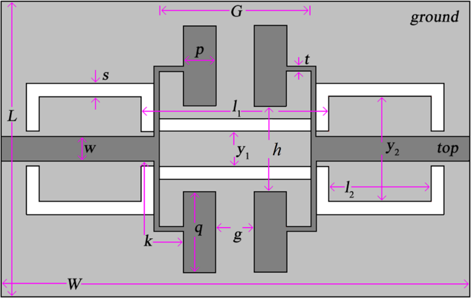
Fig. 1. Microstrip-to-CPW transition-based proposed UWB filter. Dark shade conductor and white shade etched part. All dimensions are in mm.
Proposed UWB filter
CPW-based short-circuited MMR
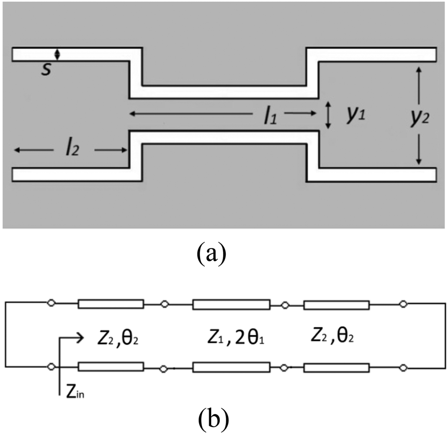
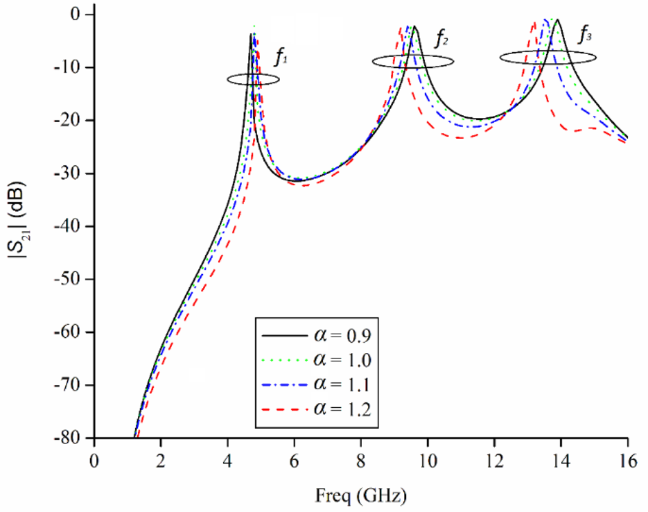
The ground plane consists of a short-circuited CPW with MMR etched in it. The MMR has two similar low-impedance (wide) sections on either side of one high-impedance (narrow) central section. The geometry and equivalent transmission line model of the CPW are depicted in Figs 2(a) and 2(b). Our analysis overlooks the two CPW-step discontinuities at the end since their effect is minimal on the UWB characteristics [Reference Gao, Zhu, Menzel and Bogelsack4]. To utilize the MMR characteristics for design of UWB-BPF, the resonant condition of all the modes must be established. In view of this, the input impedance at the left short-end (Zin), looking into the right is derived and depicted in equation (1):

Here, α = Z 1/Z 2, Z 1 is the impedance of the central section, whereas Z 2 is the impedance of the end sections. At the resonance condition, Zin = 0, and generates some set of equations which upon solving provide f 1, f 2, and f 3. For the proposed structure, the central section of MMR has dimensions, l 1 = 5.835 mm (≈λg CPW1/4), y 1 = 0.982 mm, s = 0.42 mm, for which Z 1 = Z 0(CPW1) = 51.58 Ω and θ 1 = 52.15°. Similarly, for the end sections of the MMR, Z 2 = Z 0(CPW2) = 41.4 Ω and θ 2 = 51°, corresponding to dimensions, l 2 = 3.185 mm (≈λg CPW2/8), y 2 = 3.284 mm, and s = 0.42 mm. It can be observed from above that the electrical lengths of three sections are approximately, θ 1 ≈ θ 2 ≈ θ, and α = Z 1/Z 2 = 1.2. Hence, the first three resonant frequencies evaluated are:


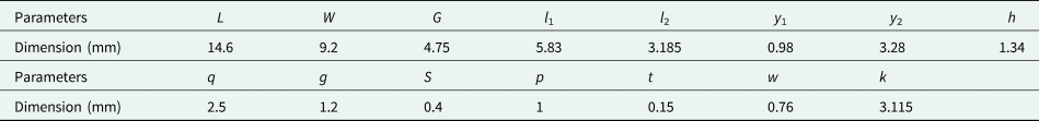
The above equations depict that the extreme frequencies (f 1, f 3) are mainly affected by the impedance ration, whereas the mid frequency (f 2) is a function of length of central section. The weak coupling response of the CPW-based MMR against variable impedance ratio is plotted in Fig. 3 from which can be observed that for reducing α, the lowest resonant mode (f 1) deviates left, whereas the higher ones (f 2, f 3) shift right.

Fig. 2. (a) Geometry of the MMR-based CPW. (b) Equivalent transmission line model.

Fig. 3. Weak coupling response for a variable impedance ratio.
Μicrostrip-to-CPW transition
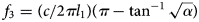
Having modeled the CPW, the objective next becomes optimizing the transition so as to generate the requisite UWB spectrum with good frequency characteristics such as minimum insertion loss and multiple TZs. The transition coupling is of capacitive nature and maximum coupling at the central UWB frequency (6.85 GHz) can be achieved by matching the characteristic impedances of the microstrip line with that of CPW i.e. Z 0(microstrip) = 2Z 0(CPW1) [Reference Baik, Lee and Kim6]. In the structure under consideration, Z 0(CPW1) = 51 Ω, and for t = 0.15 mm, Z 0(microstrip) = 81 Ω. Ideally Z 0(microstrip) = 102 Ω would have best suited the above relation, however, 81 Ω is used because it provides wider bandwidth, proper upper TZ and spurious free stopband with a negligible effect on other frequency characteristics as depicted in Fig. 4. Also, for Z 0(microstrip) = 102 Ω, the thickness of microstrip lines, t = 0.12 mm is little difficult to fabricate. From the simulated response of Fig. 4, it can be observed that the passband extends from 3.05 to 10.7 GHz with return/insertion loss better than 15/0.54 dB. The two TZs at 0.95 and 11.7 GHz provide a sharp roll-off >34 and 48 dB/GHz respectively at lower and upper passband edges. The third TZ at 16 GHz ensures a spurious-free stopband with attenuation >25 dB.
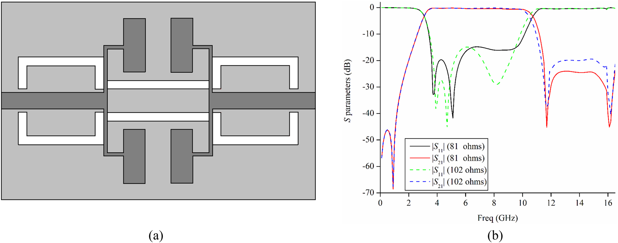
Fig. 4. (a) Architecture of the basic UWB-BPF. (b) Comparative frequency characteristics for variable impedance of CPW.
The other parameters can be altered to tune the frequency characteristics of the basic UWB-BPF. For example, Figs 5(a) and 5(b) depict the variation of frequency response for vertical height (h) and length of the central section of the CPW, y 1. It can be observed that variation in vertical separation (h) alters the TZs located at the higher passband end and in stopband without affecting the position of lower TZ. The fine tuning of y 1 brings about changes in impedances Z 1 which enhances the passband and stopband characteristics of our proposed structure. Also, the horizontal separation (g) controls the position of all three TZs, as well as selectivity at lower and upper passband/stopband edges. For small values of g, the two roll-offs at passband/stopband edges show increased selectivity but at the cost of reduced stopband width due to the presence of transmission poles (TPs) at around 12 and 15.5 GHz. However, for optimum value of g = 1.2 mm, we get the requisite UWB passband width as well as increased stopband, due to suppression of TPs at 12 and 15.5 GHz respectively. Increasing g beyond this again brings about a deterioration in frequency response. The optimized dimension of the UWB-BPF is provided in Table 1.
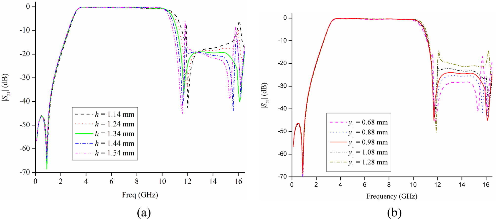
Fig. 5. Variable transmission characteristics for (a) h and (b) y 1.
Table 1. Optimized dimensions of the proposed UWB-BPF

Implementation of notches across the passband
To the basic UWB-BPF developed above, multiple FSRRs are appended on the top plane close to the feed line. These FSRRs develop notches (TZs) which are placed at frequencies of interest in the passband. The position of notch (TZ) is a function of the FSRR length and given by the formula:

Figure 6(a) depicts the tunability range of the FSRR for its variable length. For our design, FSRRs of appropriate lengths are selected to circumvent interferences at 5.2 GHz (WLAN) and 8.1 GHz (X band). The optimized dual-notched band response of the proposed BPF is depicted in Fig. 6(b), from which it can be observed that passband has a frequency spread from 3 to 10.65 GHz. Multiple TZs are observed, two at the passband edges (0.9 and 11.8 GHz) and two within it (5.2 and 8.1 GHz). The TZs have attenuation of at least 20 dB. The passband insertion/return loss is better than 0.32/15 dB (except for the dual notches). The stopband has an attenuation of 22 dB until 16 GHz. At their respective frequency of resonance, the respective FSRRs are tightly coupled to the BPF, as evident from their current distributions in Fig. 7. The FSRRs have high current concentration at the dual notch frequencies of 5.2 and 8.1 GHz, respectively, which represents their affect in generating those TZs

Fig. 6. (a) Variable position of passband TZs for different lengths of the FSRR. (b) Optimized frequency characteristics of the proposed dual-notched UWB-BPF.
Fig. 7. Current distribution in the BPF at (a) 5.2 GHz and (b) 8.1 GHz.
Experimental verification
To verify the predicted simulated performance, the structure is fabricated and its response measured using an Agilent Vector Network Analyzer N5230A. Figure 8(a) shows the measured passband frequency characteristics which extend from 3.06 to 10.73 GHz with insertion loss <1.4 dB and return loss >13 dB. Most of the structures do not report insertion loss due to their poor frequency characteristics [Reference Chu and Huang9, Reference Wei, Chen, Wang and Shi13–Reference Liu, Yin, Yang, Jing and Sun16], whereas few [Reference Song, Yang and Geyi18, Reference Ghazali, Sazid and Pal21] have very high insertion loss. Stopband observed is spurious free until 16 GHz with attenuation >22.6 dB. The dual passband notches are located at 5.28 and 8 GHz with attenuation better than 19 dB. From Fig. 8(b), it is observed that the measured group delay shows minimum variation (0.24–0.38 ns) in the passband indicating good linearity. The variations in simulated and measured data are possibly due to loss in two SMA connectors and finite substrate size. The discrepancy in IL can be attributed to the human error involved in fabrication which might have increased/decreased the thickness of conductor/slot lines during the etching process. This in turn would have varied the impedances of Z 0(microstrip) and Z 0(CPW1), thereby not satisfying the necessary condition of Z 0(microstrip) = 2Z 0(CPW1) [Reference Baik, Lee and Kim6]. The data measured are in reasonable agreement with the simulated response and also accords with the FCC-defined UWB mask for indoor wireless communication. The designed filter is less than one guided wavelength at central UWB frequency (6.85 GHz) which depicts its miniaturized architecture.

Fig. 8. Comparative BPF frequency responses: (a) S parameters and (b) group delay.
The proposed structure is compared with other dual-notched UWB filters in Table 2. It can be observed from the last column of the table that the proposed structure is compact compared to other studies [Reference Ghazali and Singh8, Reference Wu and Chen10, Reference Nouri, Nourinia, Ghobadi, Alizadeh and Mohammadi11, Reference Gandamalla, Marathe and Kulat12, Reference Liu, Yin, Sun, Fan and Ren14, Reference Liu, Yin, Yang, Jing and Sun16, Reference Song, Yang and Geyi18, Reference Zheng, Pan and Jiang20, Reference Ghazali, Sazid and Pal21]. The proposed structure possesses TZs at both passband edges unlike most [Reference Ghazali and Singh8, Reference Nouri, Nourinia, Ghobadi, Alizadeh and Mohammadi11–Reference Liu, Yin, Yang, Jing and Sun16, Reference Song, Yang and Geyi18–Reference Zheng, Pan and Jiang20], whereas, others [Reference Chu and Huang9, Reference Wu and Chen10, Reference Song and Xue17] possess TZs at either of the passband edges. This lack of TZs causes their frequency characteristics to degrade. Most of the structures reported have complex geometry due to the presence of vias [Reference Nouri, Nourinia, Ghobadi, Alizadeh and Mohammadi11–Reference Liu, Yin, Yang, Jing and Sun16, Reference Song, Yang and Geyi18, Reference Zheng, Pan and Jiang20] or limitation in fabrication caused by minimum dimension [Reference Wu and Chen10, Reference Song and Xue17]. Our proposed BPF is simple to design due to the absence of vias and limitation of minimum dimension.
Table 2. Comparison of the proposed band notched filter with other known dual notched structures.
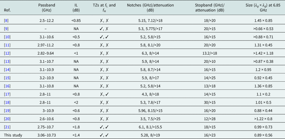
Ref., references; IL, insertion loss in the passband (excluding the notches); TZs at f L and f H, TZs at lower and upper passband edges.
Conclusion
The paper proposes a miniaturized dual-notched UWB filter based on the microstrip-to-CPW transition technology. The short-circuited MMR in ground is excited to equally space its resonant modes within the UWB passband and the coupling of microstrip-to-CPW transition is optimized to generate UWB response with good frequency characteristics. The presence of dual TZs at the passband edges improves the filter selectivity whereas a third TZ provides a spurious free stopband. As such, an UWB-BPF with good frequency characteristics having improved insertion loss/return loss (<0.26 dB/>15 dB) and linear group delay is achieved. Later multiple FSRRs are embedded into the BPF to deploy dual passband TZs so as to circumvent possible interferences. The proposed structure being a complete package of compactness and good frequency characteristics calls for its effectiveness in application to modern era UWB communication systems.
 Abu Nasar Ghazali received his B.Tech. degree in Electronics & Communication Engineering (ECE) from SRM University, Chennai, in 2008 and his M.E. degree in Microwave Engineering from the Birla Institute of Technology (BIT) Mesra, in 2010 where he was a GATE scholar. He completed his doctorate in 2014 from BIT Mesra. He worked as an Assistant Professor in the Department of ECE at the Manav Rachna College of Engineering, Haryana, in 2010 and worked as an Assistant Professor at the BIT Mesra, Patna campus. Currently, he is an Assistant Professor (II) in the School of Electronics Engineering, at the Kalinga Institute of Industrial Technology (KiiT), Deemed University, Bhubaneswar, India. He is an Associate member, The Institution of Engineers (IEI), India, and member of IEEE. He has published quite a few papers in peer reviewed journals and conferences. His main research interests are UWB filters, UWB antennas, defected ground structures, microstrip filters, and microwave circuit components.
 Mohammad Sazid received his B.Tech. degree in Electronics & Communication Engineering (ECE) from Uttar Pradesh Technical University in 2011 and his M.E. degree in Wireless Communication Engineering from BIT Mesra, in 2015 where he was a GATE scholar. He is currently working as an Assistant Professor in the Department of ECE at the Noida Institute of Engineering & Technology. He is also pursuing his doctorate from the Delhi Technological University (DTU), New Delhi. He has published several papers in SCI journals. His main research interests are UWB filters and passive microwave circuit components.