I. INTRODUCTION
Impedance transformer (IT) is one of the basic elements employed for the design of many radiofrequency (RF)/microwave systems. The main aim of the IT/matching network is to minimize the reflection between the connected circuits. In addition, it provides advantages such as maximum power transfer, high linearity, and low noise level. Therefore, IT finds large applications in antenna feed lines, mixers, microwave amplifiers, power dividers, etc. The conventional λ/4 microstrip line has been extensively used, but it can only be operated at single frequency and difficult in implementation for large load impedances. To compete with advanced communication system with multi-standard applications, it is essential to convert a single-frequency IT to a multi-frequency IT. Therefore, the design of multi-band ITs (MBITs) with ultra-high transforming ratio (UHTR) become unique challenge for many researchers. The particular use of multi-band matching network with UHTR can be found in the design of multi-band power amplifier and rectenna. In the case of rectenna design for RF energy harvesting application, the real-part of input impedance of diode for rectification could be very high (>400 Ω), especially at lower input powers [Reference Sun, Guo, He and Zhong1, Reference Yang, Jiang, Elsherbeni, Yang and Wang2]. Hence, this high input impedance should be matched to a real source of 50 Ω. Furthermore, in any high-frequency power-amplifier design, improper impedance matching will degrade the stability and reduce the circuit efficiency. In multi-band amplifier design, this consideration is even more critical. The problem occurs because the resonated impedance may be more than 500 Ω and reducing this to 50 Ω is a key challenge (http://www.nxp.com/products/rf/rf-amplifiers-low-medium-power:MC_50961; https://www.minicircuits.com/WebStore/Transformers.html). Hence, the design of dual-band matching network with UHTR has a great demand in the wireless industry today.
To surpass these issues, several dual-band ITs (DBITs) are developed for real as well as complex loads [Reference Chuang3–Reference Chow and Wan11]. To deal with the frequency-dependent complex loads, DBITs have been designed employing two-section shunt stubs [Reference Chuang3], T-type network [Reference Nikravan and Atlasbaf4], π-model [Reference Manoochehri, Asoodeh and Forooraghi5], T-shaped coupled line [Reference Barik, Bishoyi and Karthikeyan6], transmission line with shunt stubs [Reference Chuang and Wu7], coupled line with open/short stub [Reference Barik, Siddiqui, Kumar and Karthikeyan8], T-network, [Reference Maktoomi, Hashmi and Ghannouchi9] and π/T-type network [Reference Rawat and Ghannouchi10]. The DBITs based on the two-section transmission line [Reference Chow and Wan11–Reference Orfanidis14] are used to match real loads with 50 Ω source. Many transformers are designed to operate at single frequency for small [Reference Wang, Ohira and Ma15, Reference Wang, Ma, Sakagami, Mase and Yoshikawa16] and large load impedances [Reference Nguyen, Ang and Ng17–Reference Wu and Zhu23]. An IT with transforming ratio of 3.4 has been developed by employing coupled three-line [Reference Nguyen, Ang and Ng17]. In [Reference Ang, Lee and Leong18], a coupled line has been used to design an IT with transforming ratio of 3.4. The modified coupled-line IT has been reported for a transforming ratio of 5 in [Reference Chen, Hou and Tang19]. A broadband IT [Reference Ehsan, Hsieh, Moseley and Wollack20] has been demonstrated for an impedance transforming ratio of 5. A wideband IT with transforming ratio of 5 has been developed using coupled line and open-ended stub [Reference Kim, Chaudhary and Jeong21]. In [Reference Kim, Chaudhary and Jeong22], a coupled-line IT with bandpass characteristic has been designed. Two and three sections short-ended coupled lines have been employed to develop a wideband IT for UHTR of 20 in [Reference Wu and Zhu23]. Recently, two quad-band matching networks have been developed for UHTR [Reference Barik and Karthikeyan24, Reference Barik and Karthikeyan25]. To meet the present day demand for wireless systems on design of multi-band devices, it is necessary to transfer single-band IT to MBIT for large source/load impedances.
In this paper, the design of ultra-high transforming DBIT is presented. Our main effort to match large real loads to a 50 Ω source at two different frequencies. The design equations are derived analytically to obtain the dual-band operation. To validate the proposed topology, three types of DBIT with different transforming ratios of 10, 20, and 30 are designed, fabricated, and tested. To prove the flexibility of the proposed transformer, different frequency ratios (two operating frequencies can be chosen arbitrarily) are considered for all the examples. The measured return loss is better than 15 dB at each operating frequency. Furthermore, the proposed idea for matching a complex load at two different operating frequencies is validated numerically. In addition, a tri-band matching network (TBMN) for UHTR is obtained by adding a stepped impedance section to the proposed structure.
II. ANALYSIS OF THE PROPOSED DBIT
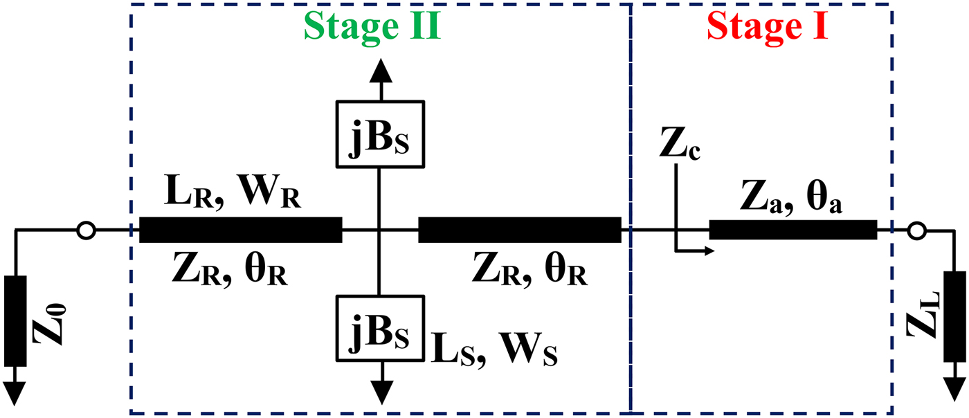
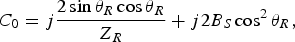
As depicted in Fig. 1, the dual-band topology consists of two series transmission lines (Z R , θ R ) with two short-ended stubs (Z S , θ S ) shunted at the center. The S-parameters of the proposed dual-band network can be computed as equation (1), from the ABCD parameters:
 $$S_{11} = \displaystyle{{rZ_L A_0 + r^2 B_0 - Z_L^2 C_0 - rZ_L D_0} \over {rZ_L A_0 + r^2 B_0 + Z_L^2 C_0 + rZ_L D_0}},$$
 $$S_{21} = \displaystyle{{2rZ_L} \over {rZ_L A_0 + r^2 B_0 + Z_L^2 C_0 + rZ_L D_0}},$$
 $$\angle S_{21} = - \displaystyle{\pi \over 2} + \mathop {\tan} \nolimits^{ - 1} \left[ {\displaystyle{{2rZ_L A_0 B_0} \over {r^2 B_0^2 + Z_L^2 - Z_L^2 A_0^2}}} \right],$$
 $$A_0 = D_0 = \mathop {\cos} \nolimits^2 \theta _R - 2B_S Z_R \sin \theta _R \cos \theta _R - \mathop {\sin} \nolimits^2 \theta _R,$$
 $$B_0 = j2Z_R \sin \theta _R \cos \theta _R - j2B_S Z_R^2 \mathop {\sin} \nolimits^2 \theta _R,$$
 $$C_0 = j\displaystyle{{2\sin \theta _R \cos \theta _R} \over {Z_R}} + j2B_S \mathop {\cos} \nolimits^2 \theta _R,$$
 $$r = \displaystyle{{Z_L} \over {Z_0}}. $$
Fig. 1. Schematic representation of the proposed dual-band impedance transformer.
And the electrical lengths of the proposed network can be written as:
 $$\theta _R = \displaystyle{{n_1 \pi f_1} \over {f_1 + f_2}}, $$
 $$\theta _S = \displaystyle{{n_2 \pi f_1} \over {f_1 + f_2}}. $$
Here n 1 and n 2 are integers.
As the proposed topology is made equivalent to a λ/4 transmission line having characteristic impedance of
 $\sqrt r Z0$
,
$\sqrt r Z0$
,
 $\angle S_{21} $
is set to 90°, the numerator of equation (1c) should be zero and reduced to A
0 = 0, which implies:
$\angle S_{21} $
is set to 90°, the numerator of equation (1c) should be zero and reduced to A
0 = 0, which implies:
 $$B_S = \displaystyle{{\cos 2\theta _R} \over {Z_R \sin 2\theta _R}}, $$
 $$Z_S = - \displaystyle{{\sqrt r Z_0 \tan 2\theta _R \tan \theta _S} \over {\tan \theta _R}}. $$
To obtain the dual-band operation, the proposed structure should satisfy another condition, which is given as:
 $$B_0 = j\sqrt r Z0 = jZ_{eq}. $$
Solving equations (2b) and (8), we get
 $$Z_R = \displaystyle{{\sqrt r Z0} \over {\tan \theta _R}}. $$
In order to design a UHTR-DBIT, a simple synthesis approach is summarized as follows:
-
(1) Select the source (Z 0) and load (Z L ) impedances. For Z 0 = 50Ω,
 $Z_{eq} = 50\sqrt r \Omega $
, where r = Z
L
/Z
0.
$Z_{eq} = 50\sqrt r \Omega $
, where r = Z
L
/Z
0. -
(2) Choose two operating frequencies f 1 and f 2, then compute the electrical lengths θ R and θ S using the equations (4) and (5), respectively, by choosing appropriate values of n 1 and n 2.
-
(3) For compactness, the value of n 2 is chosen as 1.The smaller and larger frequency ratios can be obtained by selecting n 1 = 1 and n 1 = 2, respectively.
-
(4) The characteristic impedances Z S and Z R can be obtained from the equations (7) and (9), respectively.
-
(5) Check whether the calculated values of Z S and Z R can be realizable in microstrip technology. If it is unrealizable, go back to step 2 and increase the values of n 1 and n 2.
-
(6) The physical parameters of the proposed network can be evaluated at the first operating frequency f 1.
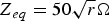
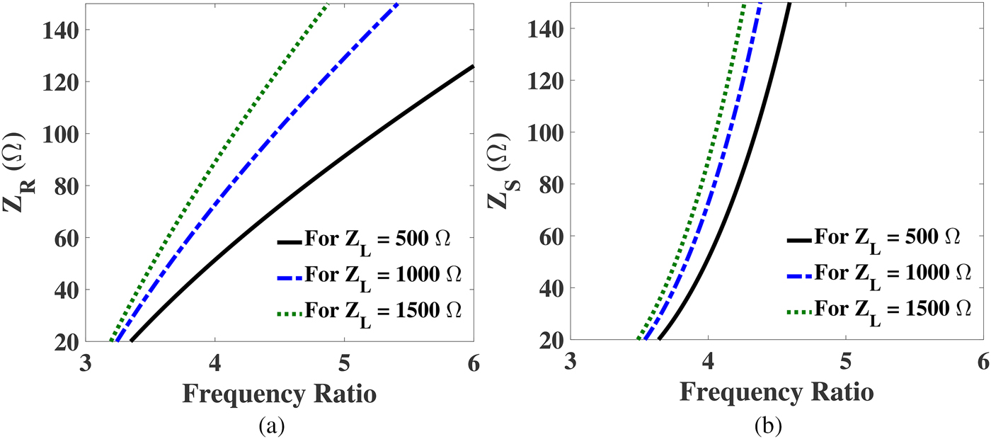
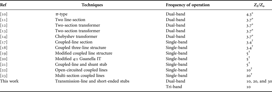
To design dual-band microwave components for all commercial dual-band applications, it is essential for a technique to provide smaller as well as larger frequency ratios, in which most of the popular wireless standards such as GSM, GPRS, WiMAX, WLAN, and Bluetooth can be covered. To calculate the realizable frequency ratios of the proposed UHTR-DBIT, the transcendental equations (7) and (9) are solved graphically for different load impedance values (Z L ). Figure 2 illustrates the impedance values Z R and Z S for smaller frequency band ratios. Similarly, the impedance values Z R and Z S for larger frequency band ratios are plotted in Fig. 3. We considered 0.8 thick FR4 substrate having dielectric constant of 4.4 for all these calculations. This implies the limitation of impedance values for microstrip technology is 20–120 Ω. For a transforming ratio of 10, i.e. Z L = 500 Ω, the smaller and larger frequency ratios obtained from Figs 2 and 3 are 1.6–2.08 and 3.64–4.45, respectively. The calculated frequency band ratios for different load impedance values are depicted in Table 1. From the table, it is observed that the proposed UHTR-DBIT is suitable for many popular communication standards and feasible for inclusion in most of the RF/microwave systems design. Table 2 depicts the design parameters required to implement a DBIT with transforming ratio of 10 and frequency band ratio of 2 for the proposed unit and previously reported schematics. As seen in Table 2, the impedance values are beyond the practical realization limits of the microstrip technology. Therefore, the topologies reported in [Reference Barik, Bishoyi and Karthikeyan6–Reference Rawat and Ghannouchi10] are not suitable for UHTR. Hence, we proposed a new DBIT and its mathematical modeling to obtained the larger transforming ratio.
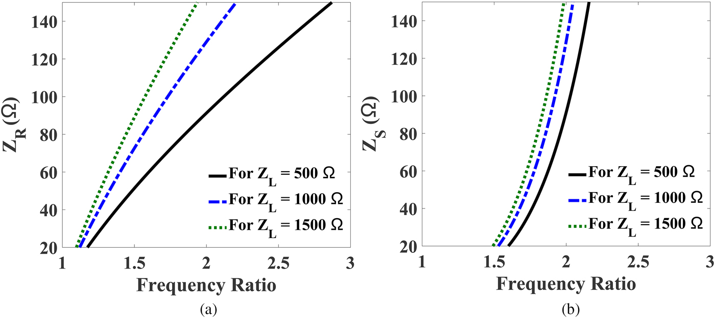
Fig. 2. The impedance values of the proposed DBIT for different load (Z L ). (a) Plot of Z R versus smaller frequency ratios (f 2/f 1) and (b) plot of Z S versus smaller frequency ratios (f 2/f 1).

Fig. 3. The impedance values of the proposed DBIT for different load (Z L ). (a) Plot of Z R versus larger frequency ratios (f 2/f 1) and (b) plot of Z S versus larger frequency ratios (f 2/f 1).
Table 1. Calculation of the realizable frequency band ratios.
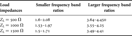
Table 2. Design parameters of the proposed unit and previously reported structures.
a, The characteristic impedance values are beyond the realization limits of the microstrip technology; b, not suitable for UHTR; c, suitable for UHTR.
III. DESIGN OF THE UHTR-DBIT
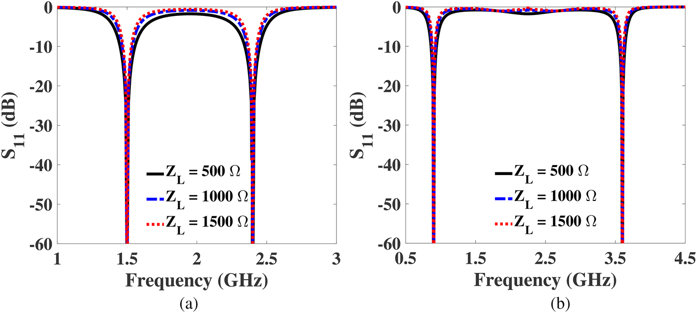
In this section, two examples of UHTR-DBITs for smaller and larger frequency band ratios are designed and simulated to validate the proposed idea presented in the above section. Specifically, the load impedances of 500 Ω (r = 10), 1000 Ω (r = 20), and 1500 Ω (r = 30) are considered to match a source impedance of 50 Ω. Based on the closed form equations, the design parameters of the proposed DBIT with different transforming ratios for smaller and larger frequency band ratios are computed and listed in Table 3. Theoretically calculated S 11 of the DBIT for smaller and larger frequency band ratios (f 2/f 1) are depicted in Fig. 4. The calculated S 11 is well below −20 dB, which proves good matching between source and load impedances at the two arbitrary frequencies. Furthermore, the bandwidth of a DBIT is a crucial parameter that needs to be focused. In the design of dual-band RF systems, it is necessary to produce significant amount of bandwidth for practical applications. In practice, the bandwidth of the transformer increases/decreases for less mismatched load (as Z L becomes closer to Z 0) and more mismatched load (as Z L becomes far to Z 0), respectively [Reference Pozar26]. Hence, the behavior of the load in the design of the proposed dual-band transformer is illustrated in Fig. 4. From the figure, It is observed that the bandwidth decreases with increasing load. It is also seen that the bandwidth is more than 100 MHz (considering S 11 < − 10 dB), which is suitable for most of the application. Therefore, the proposed DBIT provides flexible solutions for implementation of very large impedance transforming ratio and can be applied to design microwave devices, such as amplifiers, power dividers, and antennas.

Fig. 4. Theoretically calculated S 11 of the DBIT with transforming ratios of 10, 20, and 30. (a) For a smaller frequency band ratio of 1.6 and (b) for a larger frequency band ratio of 4.
Table 3. Design parameters of the proposed UHTR-DBIT for smaller and larger frequency ratios.
IV. DUAL-BAND MATCHING NETWORK FOR A COMPLEX LOAD (R 1 + jX 1)
The proposed analysis is applicable for a complex load impedance by adding one transmission line to the DBIT network as shown in Fig. 5. In the above section, we have discussed the design of dual-frequency IT for real load impedances. Therefore, this section extends the application scope of dual-band matching network for a complex load impedance. In order to validate numerically, we have considered a complex impedance of Z L = R 1 + jX 1Ω to match with the source impedance of 50 Ω. The design of DBIT for complex load consists of two steps. Firstly, a transmission line with characteristic impedance of Z a and electrical length of θ a is used to convert the complex load into a real impedance of Z c as shown in stage I of Fig. 5. Finally, the real value is transformed by the proposed dual-band matching network. The closed form design formulas for stage I can be written as:
 $$\theta _a = \mathop {\tan} \nolimits^{ - 1} \left[ {\displaystyle{{\sqrt {4 + \left( {\displaystyle{U \over {Z_a X_1}}} \right)^2} \pm \displaystyle{U \over {Z_a X_1}}} \over 2}} \right],$$
 $$Z_c = \displaystyle{{R_1^2 + \left( {X_1 + Z_a \tan \theta _a} \right)^2} \over {R_1 \left( {1 + \mathop {\tan} \nolimits^2 \theta _a} \right)}}.$$
where
 $$U = R_1^2 - Z_a^2 + X_1^2. $$

Fig. 5. Schematic layout of the proposed dual-band matching network for a complex load.
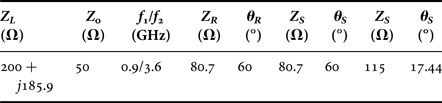
For a given value of Z L = R 1 + jX 1 and assuming the realizable value of Z a , the value of θ a and Z c can be computed from equations (10) and (11), respectively. As an example, the load impedance Z L and the value of Z a are considered as 200 + j185.9 and 115 Ω. The values of Z c and θ a are calculated as 390.73 Ω and 17.44°. For Z c = 390.73 Ω, the value of Z eq is computed as 139.77 Ω, and the corresponding design parameters of the dual-band matching network are listed in Table 4. Figure 6 presents the circuit simulated return loss performance of the dual-band transformer for a complex load. From the figure, it is seen that the return loss is more than 15 dB at each frequency band. Hence, the proposed dual-band design is also applicable for a complex load impedance.

Fig. 6. Circuit simulated return loss of the proposed dual-band matching network for a complex load (200 + j185.9 Ω).
Table 4. Design parameters of the proposed DBIT for a complex load.
V. DESIGN OF TRI-FREQUENCY MATCHING NETWORK
In this section, we have explored the multi-band characteristic of the proposed structure and designed a TBMN for a transforming ratio of 10. To obtain the tri-band operation, the proposed DBIT is slightly modified by decomposing a short circuited stub into a stepped impedance section as shown in Fig. 7. In the modified structure, the green-colored network is used to obtain dual-frequency operation (f 1 and f 2) and the stepped impedance structure (red-colored) is employed to achieve third operating frequency f 3. This stepped impedance will not meddling to the operating frequencies f 1 and f 2. Hence, the modified network is capable of producing tri-frequency characteristic. The analysis of the proposed TBMN is based on the following steps.
-
(a) To obtain dual-frequency operation, the design parameters of the green-colored structure are computed based on the procedure discussed in Section II.
-
(b) A detailed analysis is proposed to achieve third operating frequency (f 3).
-
(c) The design parameters of the red-colored network is derived in such a way that it will provide Z eq at f 3 and infinity at two other frequencies (f 1 and f 2).
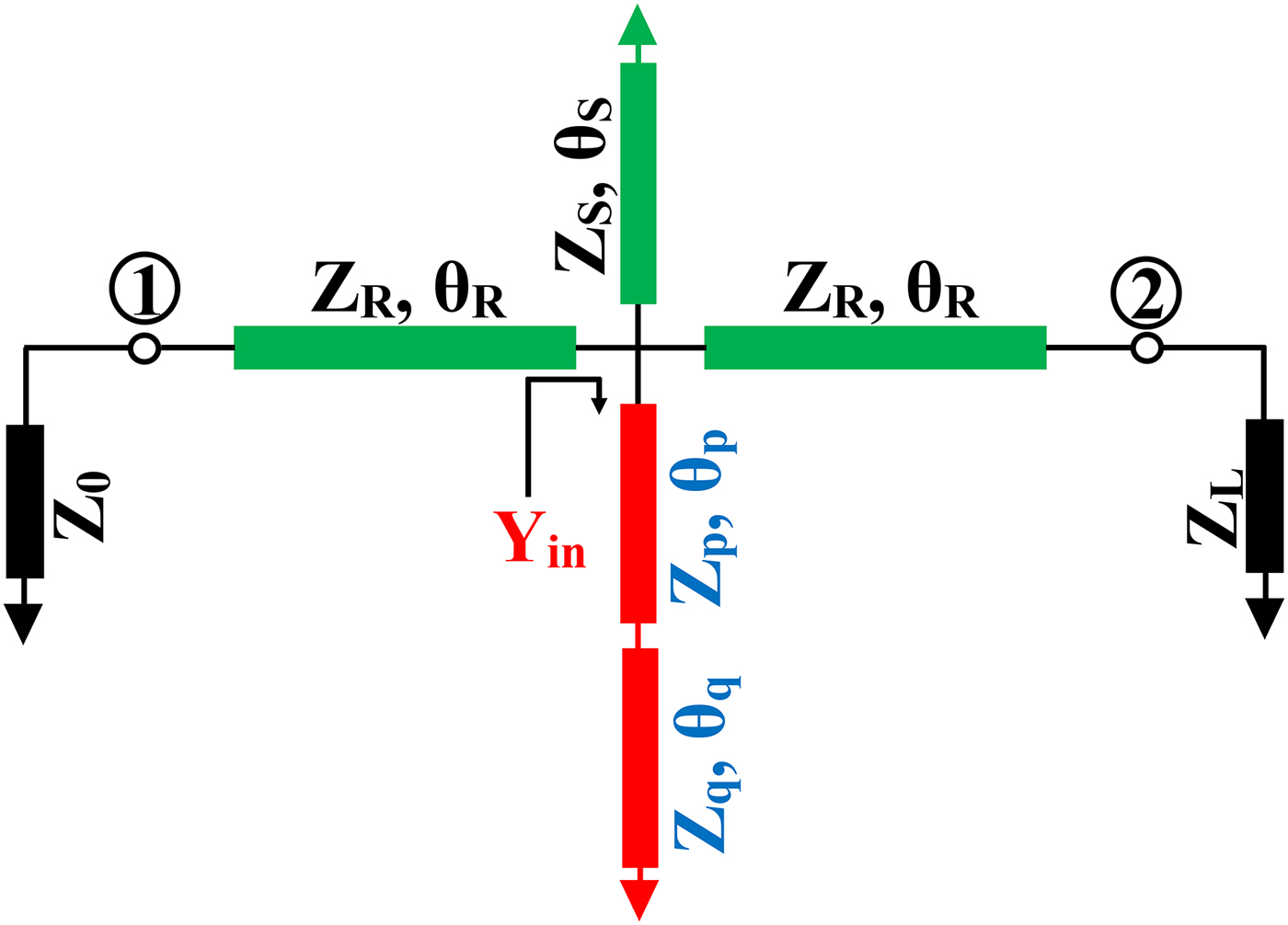
Fig. 7. Schematic representation of the proposed tri-band matching network.
Based on the synthesis procedure in Section II, the value of Z p and Z q are computed as:
 $$Z_R = \displaystyle{{Z_{eq}} \over {\tan \theta _R}}, $$
 $$Z_S = - \displaystyle{{Z_R} \over 2}\tan 2\theta _R \cot \theta _S, $$
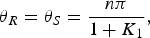 $$\theta _R = \theta _S = \displaystyle{{n\pi} \over {1 + K_1}}, $$
where
 $$K_1 = \displaystyle{{f_2} \over {f_1}}. $$
After achieving dual-frequency characteristic, the third operating frequency is obtained by employing the stepped impedance structure. This network is equivalent to a λ/4 transmission line (Z eq ) at f 3 without interrupting the dual-frequency characteristic of the green-colored structure. Thus, the desired TBMN will be obtained upon the satisfaction of these conditions. To validate the fact, the input admittance of the stepped impedance structure must be zero at f 1 and f 2, i.e.
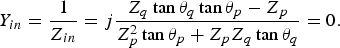 $$Y_{in} = \displaystyle{1 \over {Z_{in}}} = j\displaystyle{{Z_q \tan \theta _q \tan \theta _p - Z_p} \over {Z_p^2 \tan \theta _p + Z_p Z_q \tan \theta _q}} = 0.$$
By solving equation (15), we get:
 $$Z_p = Z_q \tan \theta _q \tan \theta _p, $$
where
 $$\theta _p = \theta _q = \displaystyle{{n\pi} \over {1 + K_1}}. $$
To develop a relationship between f 2/f 1 and f 3, the overall ABCD matrix of the proposed TBMN structure is equated with a λ/4 transmission line with characteristic impedance of Z eq as yield in equation (17).
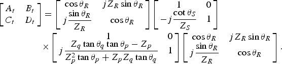 $$\eqalign{\left[ {\matrix{ {A_t} & {B_t} \cr {C_t} & {D_t} \cr}} \right] & = \left[ {\matrix{ {\cos \theta _R} & {jZ_R \sin \theta _R} \cr {j\displaystyle{{\sin \theta _R} \over {Z_R}}} & {\cos \theta _R} \cr}} \right]\left[ {\matrix{ 1 & 0 \cr { - j\displaystyle{{\cot \theta _S} \over {Z_S}}} & 1 \cr}} \right] \cr & {\rm \times} \left[ {\matrix{ 1 & 0 \cr {j\displaystyle{{Z_q \tan \theta _q \tan \theta _p - Z_p} \over {Z_p^2 \tan \theta _p + Z_p Z_q \tan \theta _q}}} & 1 \cr}} \right]\left[ {\matrix{ {\cos \theta _R} & {jZ_R \sin \theta _R} \cr {j\displaystyle{{\sin \theta _R} \over {Z_R}}} & {\cos \theta _R} \cr}} \right].} $$
From equation (17), we get:
 $$\eqalign{A_t & = \cos 2\theta _R \cr & \quad - \displaystyle{{Z_R} \over 2}\sin 2\theta _R \left[ { - \displaystyle{{\cot \theta _S} \over {Z_S}} + \displaystyle{{Z_q \tan \theta _q \tan \theta _p - Z_p} \over {Z_p^2 \tan \theta _p + Z_p Z_q \tan \theta _q}}} \right],}$$
 $$\eqalign{& B_t = jZ_R \sin 2\theta _R \cr & \quad - Z_R^2 \mathop {\sin} \nolimits^2 \theta _R \left[ { - \displaystyle{{\cot \theta _S} \over {Z_S}} + \displaystyle{{Z_q \tan \theta _q \tan \theta _p - Z_p} \over {Z_p^2 \tan \theta _p + Z_p Z_q \tan \theta _q}}} \right].}$$
Hence, by equating, A t = 0 and B t = ±jZ eq , the following equations are obtained:
 $$\left[ { - \displaystyle{{\cot \theta _S} \over {Z_S}} + \displaystyle{{Z_q \tan \theta _q \tan \theta _p - Z_p} \over {Z_p^2 \tan \theta _p + Z_p Z_q \tan \theta _q}}} \right] = \displaystyle{{2\cot 2\theta _R} \over {Z_R}}, $$
 $$\eqalign{ & \left[ { - \displaystyle{{\cot \theta _S} \over {Z_S}} + \displaystyle{{Z_q \tan \theta _q \tan \theta _p - Z_p} \over {Z_p^2 \tan \theta _p + Z_p Z_q \tan \theta _q}}} \right] \cr & \quad = \displaystyle{{Z_R \sin 2\theta _R - Z_{eq}} \over {Z_R^2 \mathop {\sin} \nolimits^2 \theta _R}}.}$$
By solving equations (20) and (21), we can obtain:
 $$\displaystyle{{2\cot \left( {2K_2 \theta _R} \right)} \over {Z_R}} = \displaystyle{{Z_R \sin \left( {2K_2 \theta _R} \right) - Z_{eq}} \over {Z_R^2 \mathop {\sin} \nolimits^2 \left( {K_2 \theta _R} \right)}},$$
 $$\eqalign{ & \displaystyle{{Z_q \tan \left( {K_2 \theta _q} \right)\tan \left( {K_2 \theta _p} \right) - Z_p} \over {Z_p^2 \tan \left( {K_2 \theta _p} \right) + Z_p Z_q \tan \left( {K_2 \theta _q} \right)}} \cr & \quad = \displaystyle{{2\cot \left( {2K_2 \theta _R} \right)} \over {Z_R}} + \displaystyle{{\cot \left( {K_2 \theta _S} \right)} \over {Z_S}},}$$
 $$\displaystyle{{Z_p} \over {Z_q}} = \displaystyle{{\tan \left( {K_2 \theta _q} \right)\left[ {\tan \left( {K_2 \theta _p} \right) - LZ_p} \right]} \over {LZ_p \tan \left( {K_2 \theta _p} \right) + 1}},$$
where
 $$K_2 = \displaystyle{{f_3} \over {f_1}} {\rm and} L = \displaystyle{{2\cot \left( {2K_2 \theta _R} \right)} \over {Z_R}} + \displaystyle{{\cot \left( {K_2 \theta _S} \right)} \over {Z_S}}. $$
By solving equations (16) and (24), the values of Z p and Z q can be expressed as:
 $$Z_p = \displaystyle{{\tan \left( {K_2 \theta _q} \right)\tan \left( {K_2 \theta _p} \right) - \tan \theta _q \tan \theta _p} \over {L\left[ {\tan \left( {K_2 \theta _p} \right)\tan \theta _q \tan \theta _p + \tan \left( {K_2 \theta _q} \right)} \right]}},$$
 $$Z_q = \displaystyle{{Z_p} \over {\tan \theta _q \tan \theta _p}}. $$
To design a TBMN, a systematic procedure is summarized as follows:
-
• Calculate the ratio K 1 by choosing two operating frequencies (f 2/f 1). Compute the values of Z R , Z S , θ R , and θ S using equations (12) and (13).
-
• Using equation (22), the value of K 2 ( = f 3/f 1) is obtained.
-
• The values of Z p and Z q are computed using equations (25) and (26), respectively.
Initially, two operating frequencies are chosen for dual-band operation. For a load of 500 Ω, the realizable frequency ratio can be chosen between 1.76 <K
1 <2.31. After selection of two operating frequencies f
1 and f
2, the third operating frequency f
3 is calculated by using equation (22). For example, when K
1 = 2.3, the equality of the equation (22) is satisfied for the value of K
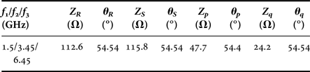
2 = 4.3. To validate the theoretical design process, a tri-band transformer operating at 1.5/3.45/6.45 GHz is designed and simulated. Based on the synthesis procedure, the design parameters are calculated for a transforming ratio of 10 (Z
L
= 500 Ω). For
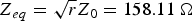 $Z_{eq} = \sqrt r Z_0 = 158.11\,\Omega $
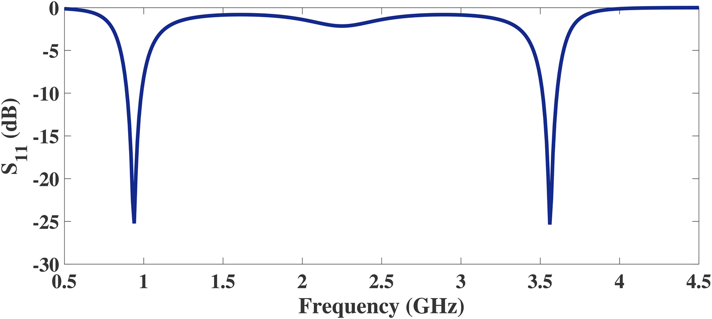
, the parameter values are listed in Table 5. Figure 8 depicts the theoretical return loss of the TBMN for a transforming ratio of 10. From the figure, it is seen that the S
11 is well below −20 dB at each frequency band. This implies the proposed network is capable of transferring a very high load to a source of 50 Ω at three different operating frequencies.
$Z_{eq} = \sqrt r Z_0 = 158.11\,\Omega $
, the parameter values are listed in Table 5. Figure 8 depicts the theoretical return loss of the TBMN for a transforming ratio of 10. From the figure, it is seen that the S
11 is well below −20 dB at each frequency band. This implies the proposed network is capable of transferring a very high load to a source of 50 Ω at three different operating frequencies.
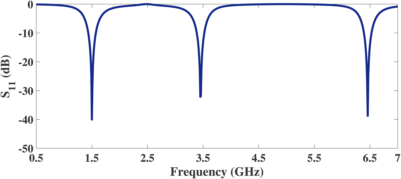
Fig. 8. Circuit simulated return loss of the proposed tri-band matching network for a transforming ratio of 10.
Table 5. Design parameters of the proposed tri-frequency matching network.

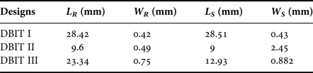
VI. FABRICATION AND MEASUREMENT
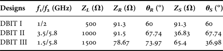
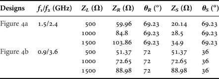
To support the circuit analysis, three DBITs with transforming ratios of 10, 20, and 30 are designed and fabricated. The load impedances Z
L
= 500, 1000, and 1500 Ω are considered to match a source impedance of 50 Ω and constructed by SMD resistors with the corresponding values. The design parameters of the UHTR-DBITs for transforming ratios of 10, 20, and 30 are computed and listed in Table 6. Based on the parameter values, the physical dimensions are calculated and depicted in Table 7. The proposed DBIT is fabricated on a low cost 0.8 thick FR4 epoxy substrate having dielectric constant 4.4, and loss tangent 0.019. The photograph of the fabricated DBITs are shown in Fig. 9. The circuit areas of the DBIT I, II, and III are
 $57.9 \times 58.1{\kern 1pt} \,{\rm mm}^2, 19.2 \times 18\,{\rm mm}^2 $
, and
$57.9 \times 58.1{\kern 1pt} \,{\rm mm}^2, 19.2 \times 18\,{\rm mm}^2 $
, and
 $46.68 \times 25.9{\kern 1pt} \,{\rm mm}^2 $
, respectively.
$46.68 \times 25.9{\kern 1pt} \,{\rm mm}^2 $
, respectively.

Fig. 9. Photograph of the fabricated UHTR-DBITs for real load impedances of Z L = 500, 1000, and 1500 Ω.
Table 6. Design parameters of the fabricated UHTR-DBITs.

Table 7. Physical dimensions of the fabricated UHTR-DBITs.
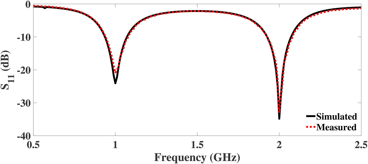
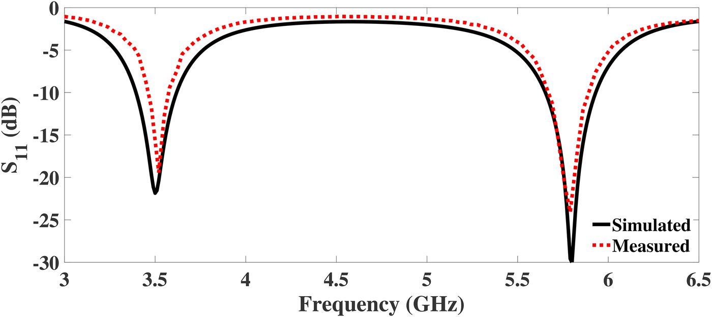
R & S ZVL vector network analyzer is used to test the fabricated DBITs. Figures 10–12 illustrate the comparison of simulated and measured return loss (S 11) of the DBIT I, II, and III, respectively. The S 11 is better than 15 dB at each operating frequency for all the fabricated devices. From the plots, it is revealed that the proposed DBITs provide excellent matching between the load impedances (Z L = 500, 1000, and 1500 Ω) and source impedance of 50 Ω at all operating frequencies. The exact values of the S 11 and bandwidth of the fabricated prototypes are illustrated in Tables 8 and 9, respectively. Comparison of the proposed work with current state of art in terms of impedance transforming ratios and frequency bands is summarized in Table 10.

Fig. 10. Simulated and measured return loss of the proposed DBIT for a real load impedance of Z L = 500 Ω.

Fig. 11. Simulated and measured return loss of the proposed DBIT for a real load impedance of Z L = 1000 Ω.
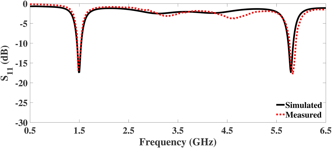
Fig. 12. Simulated and measured return loss of the proposed DBIT for a real load impedance of Z L = 1500 Ω.
Table 8. Simulated and measured S 11 comparison.
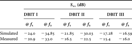
Table 9. Simulated and measured bandwidth comparison.
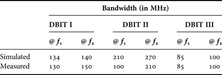
Table 10. Comparison of impedance transforming ratios with previous reported works.

* Transforming ratio is calculated based on the design equations presented in [Reference Rawat and Ghannouchi10–Reference Orfanidis14].
† Wideband impedance transformer.
VII. CONCLUSION
A new dual-band topology is proposed to design a ultra-high transforming IT. A detailed analysis has been worked out to provide exact closed form solution. Based on the derived equations, two examples of dual-band transformer working at smaller and larger frequency ratios are designed for different load impedances. Finally, three prototypes of DBIT with various transforming ratios are fabricated and verified. The measured S 11 is >15 dB at each frequency band. The tested results show excellent agreement with the simulated results. In addition to dual-band operation, we explored the multi-band characteristic of the proposed network and designed a tri-band transformer for a transforming ratio of 10. The proposed dual-frequency structure is also employed to match a complex load. Hence, the multi-band characteristic of the presented matching network is suitable in the design of multi-frequency power amplifiers, low noise amplifiers, rectification circuits, etc.
 Rusan Kumar Barik was born in Odisha, India. He received the B. Tech degree in Electronics and Tele-Communication Engineering from Biju Patnaik University of Technology, Rourkela, India in 2012 and the M. Des degree in Communication Systems Design from Indian Institute of Information Technology Design and Manufacturing, Kancheepuram, India in 2015, where he is currently working towards his Ph.D. degree. His research interests include design of multi-band microwave passive components and low noise amplifier for millimeter wave applications.
 S. S. Karthikeyan was born in Mayiladuthurai, Tamilnadu, India. He received the B.E. degree in Electronics and Communication Engineering from Bharathidasan University, Trichy, in 2001 and M.E. in Applied Electronics from Sathyabama University, Chennai, in 2005. He obtained his Doctoral Degree from the Indian Institute of Technology Guwahati, Assam, India in 2011. Currently he is working as an Assistant Professor at the Indian Institute of Information Technology, Design and Manufacturing Kancheepuram, Chennai, India. His research interests include electromagnetic bandgap substrates, microwave filters, metamaterials, microwave sensors, etc.