I. INTRODUCTION
Historically, the design of radio front-ends and their building blocks in the 60 GHz band was based on compound semiconductors due to their very high unity gain frequencies. However, since technology scaling allowed the fabrication of CMOS devices with gate lengths of 130 nm or below, ever-increasing cutoff frequencies render mm-wave radio-frequency integrated circuits (RFICs) feasible. The use of CMOS technology is especially interesting for applications that demand low cost in mass production, co-integration of digital, mixed-signal, and RF circuits to form a system on chip or, as shown in this paper, very low power consumption.
The very first 60 GHz receiver front-ends in CMOS technology by Razavi [Reference Razavi1] and Alldred et al. [Reference Alldred, Cousins and Voinigescu2] consisted only of a low-noise amplifier (LNA), a mixer, and, in the latter case, associated local oscillator (LO) and Intermediate Frequency (IF) buffers. While the receiver front-end presented by Razavi exhibits a quite low power consumption, it does not include such power-hungry elements as the LO and IF buffers and the voltage controlled oscillator (VCO) [Reference Razavi1].
More complete front-ends that also include a means to generate the LO signal were published subsequently. Although Emami et al. [Reference Emami, Doan, Niknejad and Brodersen3], Sanduleanu and Long [Reference Sanduleanu and Long4], Lee et al. [Reference Lee, Huang, Chen, Lu and Chang5], Bozzola et al. [Reference Bozzola6], and Vecchi et al. [Reference Vecchi7] present the integration of an on-chip VCO together with a down-converter, a phase locked loop (PLL) was integrated in [Reference Mitomo8, Reference Chen, Lee and Liu9]. These realizations allow a more realistic comparison of the front-end power consumption, because the trade-off between the LO-power available to the mixer and the power consumption of VCO and mixer is done on-chip.
Note that also complete 60 GHz CMOS radios have been published and are even commercially available. However, they usually are not optimized with respect to power consumption. To the best of the author's knowledge, the transceiver by Marcu et al. [Reference Marcu10] presents the lowest power consumption at this high level of integration for a 60 GHz radio.
The work presented in the following concentrates on the front-end, as it is the part mainly responsible for the circuit's power consumption [Reference Marcu10]. A comparison to circuits exhibiting a comparable level of complexity, given in Section V, shows that the results with respect to power consumption presented in this paper constitute record values. The achieved minimization is accomplished by a systematic design for low required LO-power (mixer), high efficiency (VCO), and low dissipated DC power (LNA). Furthermore, the use of a direct conversion architecture allows for a low device count and thus low complexity.
As second issue addressed by the design presented in this paper is the minimization of chip area: as many RFIC designers still follow the MMIC paradigm, mm-wave designs are often based on distributed elements for matching, which results in large circuit size and thus high fabrication cost. To minimize circuit area, however, spiral inductors shall be employed [Reference Dickson, LaCroix, Boret, Gloria, Beerkens and Voinigescu11, Reference Kraemer, Dragomirescu and Plana12]. This paper shows that if the use of spiral inductors coincides with a low complexity direct conversion architecture, a record value for the receiver front-ends circuit size can be achieved.
The remainder of this article is organized as follows: First, Section II gives an overview of the realized circuit and briefly discussed its basic building blocks and how they contribute to the front-end's low power consumption. Next, Section III shows the fabricated circuit. In Section IV, the obtained measurement results are discussed. These results are compared to the state-of-the-art in Section V. Finally, a conclusion is drawn.
II. CIRCUIT DESIGN
The receiver front-end presented in this paper consists of the in-phase branch of a direct conversion receiver. This circuit is part of a research effort aiming to integrate a complete 60 GHz I/Q transceiver front-end in 65 nm CMOS technology. While the final version of this transceiver allows receiving a quadrature-modulated signal, the presented receiver front-end only allows the reception of simpler, less spectrally efficient modulations.
The block diagram of the realized receiver front-end is illustrated in Fig. 1. Its off-chip interfaces consist of a single-ended 60 GHz RF input, a differential baseband (BB) output, and DC connections for the four bias voltages, the oscillator's control voltage, the 1 V power supply, and ground.

Fig. 1. Block diagram of the realized front-end with interfaces.
The following sub-sections discuss the key building blocks (LNA, down-mixer, VCO and baseband, and LO buffers) that constitute the receiver front-end. Their circuit schematics are given together with some key figures describing their performance. The aspects of their design that concern the front-end's power consumption are also brought up.
Standalone – versions of these blocks have been separately fabricated and measured before receiver integration. The results obtained from their measurements are published in [Reference Kraemer, Dragomirescu and Plana13] for the LNA, [Reference M Kraemer, Dragomirescu and Plana14] for the VCO, and [Reference Kraemer, Ercoli, Dragomirescu and Plana15] for the down-mixer. To integrate these building blocks to form the front-end of Fig. 1, the matching networks at their interfaces have been adapted accordingly. Furthermore, they are surrounded by grounded walls consisting of shunted metal layers that allow the isolation of adjacent building blocks.
A) The low-noise amplifier
The requirements on the low-noise amplifier are governed by the Friis equation. A simplified version, where NF LNA is the noise figure of the LNA, NF 2 the total noise figure of all subsequent circuit elements, and G LNA the gain of the LNA, reads
It illustrates that the receiver noise can be minimized only if the LNA has a low-noise figure and high gain, the latter to decrease the influence of the subsequent stages on the noise performance. To achieve the optimization of these two parameters at the same time, a two-stage cascode LNA with the schematic given in Fig. 2 is employed. Its input stage is simultaneously noise and power matched by sizing the input transistor M1 and employing inductive source degeneration [Reference Kraemer, Dragomirescu and Plana13].

Fig. 2. Circuit schematic of the employed LNA.
The cascode topology is preferred over a common-source stage in order to increase reverse isolation, which is necessary to ensure unconditional stability and parasitic LO leakage from the mixer to the antenna.
Although the LNA has a certain influence on the receiver linearity, it is the subsequent stages that are decisive in this regard. Thus, as power consumption is directly related to the linearity of the LNA (but does, in a first-order consideration, not depend on the gain of the LNA), it can be minimized by sizing the transistors to yield minimum noise (first stage) or maximum power gain (second stage) for low bias currents.
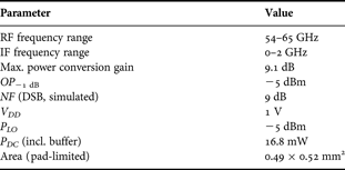
The measured performance of the standalone LNA is summarized in Table 1. It stems from a redesigned version of the LNA presented in [Reference Kraemer, Dragomirescu and Plana13] which operates at a slightly higher center frequency. An in-detail discussion of the performance of the initial LNA is given in [Reference Kraemer, Dragomirescu and Plana13].
Table 1. Performance summary of the LNA (measured values).
B) Down-conversion mixer
When designing a low-power mixer circuit, two kinds of power consumption have to be taken into account: the dissipated DC power P DC and the LO power P LO necessary for abrupt switching. Of these two powers, the latter one is by far the most expensive one in terms of overall receiver power consumption, as the on-chip oscillator used to generate the LO signal is usually of very low efficiency.
Besides power consumption, the Friis equation has to be respected, demanding high-gain and low-noise figure to minimize overall receiver performance. Furthermore, the down-mixer is the component limiting the receiver linearity, thus, it has to be optimized in this regard as well.
To find an optimum compromise between all of these requirements, the single-balanced mixer shown in Fig. 3 is employed [Reference Kraemer, Ercoli, Dragomirescu and Plana15]. An active mixer has been chosen to obtain conversion gain and limit the required LO power. The input stage is simultaneously noise and power matched as in the case of the LNA.

Fig. 3. Circuit schematic of the employed down-conversion mixer.
The most important design technique ensuring the good performance of this mixer is current bleeding by the means of the inductor L B and the resistor R S [Reference Kraemer, Ercoli, Dragomirescu and Plana15]. As part of the bias current of M1 by-passes M2 and M3, the lower transistor M1 can provide high transconductance, whereas the switching pair is made up of small transistors that require only low LO power for fast switching. Furthermore, the bleeding inductor resonates the parasitic capacitances at the terminal common to all of the transistors, thus increasing conversion gain.
Note also the use of the capacitor C 1 that short circuits the resistive loads for the LO and RF signal. This allows for high LO and RF to baseband isolation and increases linearity and conversion gain.
The presented mixer exhibits an excellent compromise between all requirements over the whole unlicensed 60 GHz band. They are discussed in [Reference Kraemer, Ercoli, Dragomirescu and Plana15] and summarized in Table 2. Note that these measurements result from a standalone version with baseband buffer (cf. Fig. 5(a)). The mixer's key performance, if a low-power receiver is desired, is the very low required LO power of only −5 dBm.
Table 2. Performance summary of the down-mixer.

C) Voltage-controlled oscillator
Rather than minimizing the DC power consumption of the VCO, its efficiency, i.e. P out/P DC, has to be optimized to achieve a low-power receiver front-end. Otherwise, subsequent, power-hungry buffer stages become necessary.
The VCO used for this purpose is given in Fig. 4 [Reference M Kraemer, Dragomirescu and Plana14]. Due to the use of a differential Colpitts architecture based on cross-coupled common-source transistors, the amplitude-limiting nonlinearity affects the behavior of the VCO only for quite high output powers. Thus, output power is higher than for other oscillator architectures at a given DC power consumption.

Fig. 4. Circuit schematic of the VCO with integrated common-drain buffer.
The VCO employs an octagonal 155 pH inductance with differential Q of 19.1 at 60 GHz in the resonator. The frequency tuning is accomplished by differentially tuned accumulation-MOS varactors. A source-follower output buffer is attached to the oscillator core.
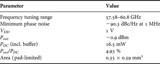
Further details on the design of the VCO are discussed together with the obtained results in [Reference M Kraemer, Dragomirescu and Plana14]. Table 3 summarizes the performance of the VCO. Its record efficiency is one of the main reasons for the very low power consumption of the entire receiver, while the limited tuning range can be optimized by optimizing the (full-custom) varactor design.
Table 3. Performance summary of the VCO [Reference M Kraemer, Dragomirescu and Plana14].

D) The LO and baseband buffers
In addition to the fundamental building blocks like LNA, mixer and oscillator, buffer amplifiers are employed in the receiver front-end. Their schematics are given in Figs 5(a) and 5(b).
The LO buffer is used to further increase the LO power level at the input of the down-mixer and to increase common-mode rejection in the LO signal path by means of the tail impedance consisting of C F and R F. It is based on a differential common-source amplifier. Due to the low LO power requirements of the mixer this buffer is not essential, but is integrated in view of a later quadrature receiver. In the receiver at hand, it is biased at very low bias current.
The baseband buffer of Fig. 5b is added to the baseband output of the mixer. It is necessary to drive the differential 100 Ω load, which is encountered if characterizing the receiver front-end using a measurement setup with instruments that exhibit single-ended 50 Ω input impedances. It is based on a current-mirror biased differential pair. The load impedances consist of an on-chip R-C load (which filters LO and RF signals) and a large off-chip inductance that allows biasing the buffer transistors without suffering from the large voltage drop that would occur if the bias current would pass by the resistors.

Fig. 5. (a) Second LO buffer. (b) Baseband output buffer.
The baseband buffer consumes 14 mW due to the large current required by the low-impedance load. In a more complete integrated receiver circuit, it shall be replaced by a variable gain amplifier with high-impedance load, achieving much lower power consumption (<5 mW) while exhibiting huge, variable gain (>50 dB).Thus, the front-end's power consumption can be considered 14 mW lower, if it is integrated with the baseband circuit.
III. THE FABRICATED FRONT-END CIRCUIT
Figure 6 shows the die photograph of the fabricated receiver frontend. Its very small size of 0.550 mm2 is essentially pad limited: the aligned circuit blocks without pads are only about 200 µm wide. This is the result of using a total of 19 compact spiral inductors for matching.

Fig. 6. Microphotograph of the fabricated CMOS receiver front-end.
The number of pads can further be reduced because multiple V DD and ground connections are provided (see the respective symbols in Fig. 6). These redundant connections are not essential for the operation of the receiver due to its low supply current (about 43 mA). Furthermore, the bias voltages could be derived from V DD in a redesigned version, allowing to remove four more pads. The part of the circuit shown at the right in Fig. 6, which consists of the differentially implemented parts, is very symmetric to reduce mismatch and improve isolation.
IV. MEASUREMENT RESULTS
The receiver front-end was characterized on-wafer using a 67 GHz single-ended 100 µm G-S-G Picoprobe to provide the RF signal and a differential G-S-G-S-G probe of the same type to measure the baseband output. The DC voltages were connected using two eyepass six-finger probes. The measurements were done using either an Anritsu MS4647A 70 GHz VNA to obtain the return loss. In this case, one of the differential baseband outputs was matched to 50 Ω by a precision load. Or, for conversion measurements, an Agilent E8257D 67 GHz synthesizer served as signal source and a LeCroy SDA813Zi 13 GHz real-time oscilloscope with spectrum analyzer functionality was connected to the circuit's differential baseband output. The loss due to cable and probes is de-embedded and 3 dB is added to the output power in case of single-ended measurements.
A) Power consumption
The receiver front-end is biased at the optimum current densities of the circuit components by applying bias voltages of V bias1 = 460 mV, V bias2 = 390 mV, V bias3 = 510 mV, and V bias4 = 540 mV. It draws about 43 mA from a 1 V supply, thus consuming P DC = 43 mW. This power consumption can be reduced by the amount contributed by the baseband buffers (i.e. ≈14 mA, cf. Section 4.4) in an integrated version, because the baseband output usually does not have to drive two 50 Ω loads but a variable gain amplifier with high-impedance inputs. Thus, VCO, LO buffers, down-mixer, and LNA together consume only 29 mW.
B) In- and output return loss
The return loss at the RF input and the baseband output of the receiver front-end were measured at the above-mentioned bias point with a control voltage of V control = 0 V, corresponding to an LO frequency of about f 0 = 57.5 GHz. However, the oscillation frequency does not have any influence on the return loss, as both input and output of the receiver are very well isolated from the LO.
The left part of Fig. 7 shows the measured excellent, broadband input match that lies below −10 dB from 53.1 GHz up to 66.0 GHz. The minimum return loss is achieved at 58.9 GHz. The measured return loss at the baseband output of the receiver front-end, shown in the right part of Fig. 7, is about −17.4 dB within the entire required baseband bandwidth of about 1 GHz, and stays below −10 dB up to 12.5 GHz.

Fig. 7. Measured in- and output return loss of the receiver front-end.
C) Frequency tuning range
As for the VCO presented above, the frequency tuning range of the receiver is about 3 GHz. However, the absolute oscillation frequencies have slightly shifted for the complete receiver. They lie between 57.0 and 60.0 GHz for a control voltage between 0.15 and −3 V. This can be explained by the different loads connected to the VCO and the fact that automatic dummy insertion was done differently between the fabrication runs of the standalone VCO and the receiver front-end.
D) Conversion gain
To measure the receiver's conversion gain, a low-power sinusoidal signal is injected at the RF port of the receiver front-end. In the lower sideband (LSB), this signal lies f IF below the carrier frequency, in the upper sideband (USB) this signal is f IF above f LO. The ratio between the received power at the differential baseband output and the injected signal power is denoted as power conversion gain G C in the following. (Note that due to the use of very high impedances at the baseband output, receivers in literature often report the voltage conversion gain [Reference Razavi1], which in these cases is considerably higher than the power conversion gain.)
Figure 8 (left) plots the conversion gain in the LSB and USB for baseband frequencies of 1 and 2 GHz. A maximum power conversion gain of 29.5 dB is achieved for a baseband frequency of f IF = 1 GHz. In agreement with the input return loss and the characteristic of the LNA, the LO frequency for which both sidebands have the same conversion gain is about 58.75 GHz. The 3 dB RF bandwidth of the receiver, which is limited by the response of the LNA, reaches from about 56.5 GHz to about 61.5 GHz, thus spanning 5 GHz in the lower part of the unlicensed 60 GHz band. The LO frequency range considered is limited by the oscillator's tuning range.

Fig. 8. Measured conversion gain G C of the receiver front-end.
Figure 8 (right) plots the conversion gain versus RF input frequency for different LO frequencies. It illustrates that within the bandwidth of 1.88 GHz around the carrier, which is required by the different standards, quite high values between 26 and 30 dB are achieved at all possible LO frequencies. For the central LO frequency of f LO = 58.5 GHz, the one-sided 3 dB baseband bandwidth is measured to be about 1.5 GHz, corresponding to a channel bandwidth of 3 GHz around the carrier. The receiver's bandwidth is not limited by the baseband circuitry or the mixer, but rather by the characteristics of the LNA, which results in the fact that input signals above and below the center frequency of 58.5 GHz experience less gain.
E) Output waveforms
To analyze the balance of the differential signal at the baseband output of the receiver, the voltage waveforms were measured for different frequencies and input powers. Figure 9 shows this signal at both baseband outputs when the frequency difference is 1 GHz. Even at this relatively high frequency, the phase shift of 180° is well maintained, while variations occur due to the phase variations of the unlocked VCO. For lower baseband frequencies, the voltage waveforms are even better balanced.

Fig. 9. Measured baseband output voltages for f LO = 58 GHz, f RF = 59 GHz, and P RF = −45 dBm.
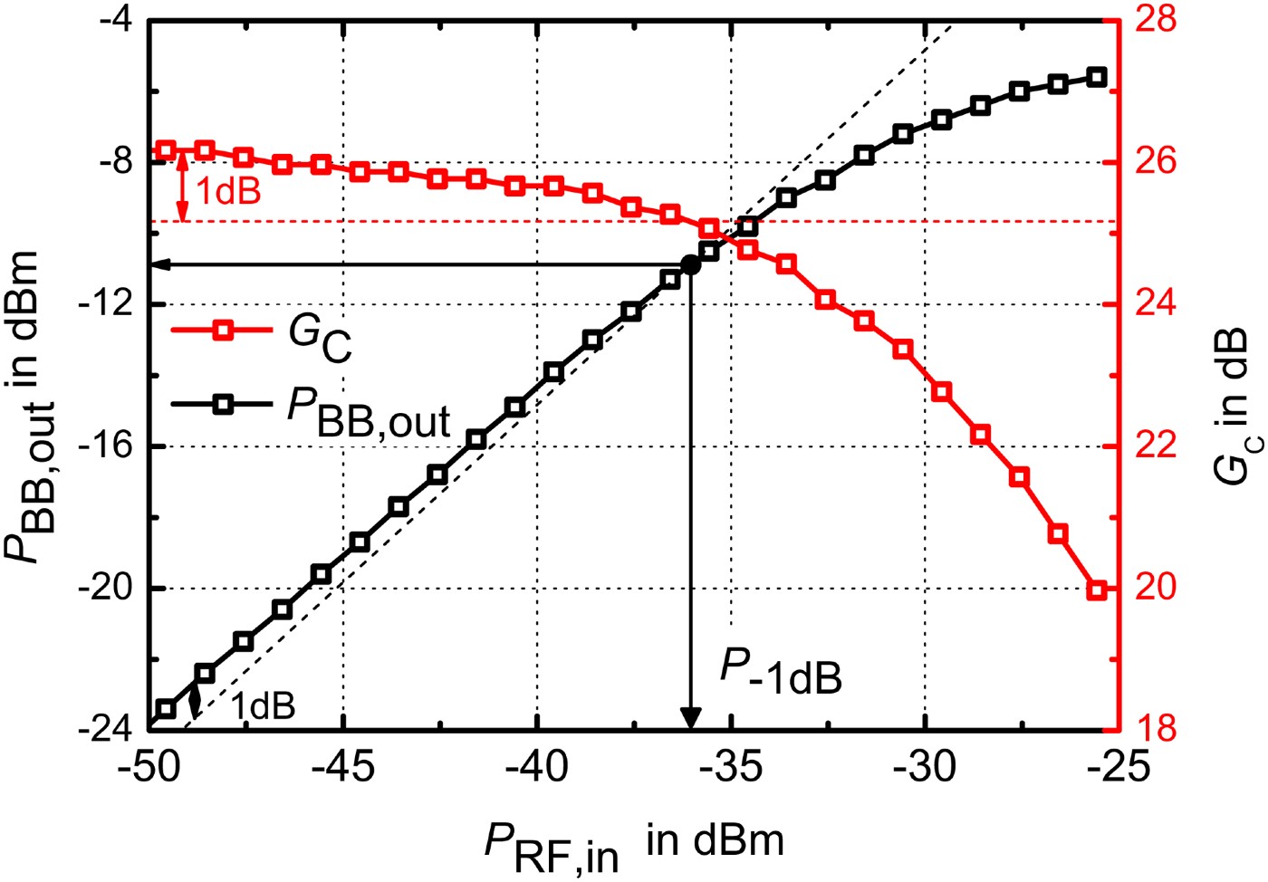
F) Linearity and noise
The linearity of the receiver front-end is characterized by its 1 dB compression point P −1 dB. Figure 10 plots power conversion gain and output power versus input power to obtain its value: it shows that the receiver achieves an output-referred compression point OP−1 dB = −11 dBm, which corresponds to an input-referred compression point of IP−1 dB = −36 dBm. This quite low value at the input of the receiver results from the high conversion gain and the moderate linearity of the output buffer. However, as both the received in-band power and the interference power level at the receiver input are expected to lie well below this value, this compression point is sufficient for a 60 GHz receiver and helps to keep power consumption low.

Fig. 10. Measured output versus input power of the receiver front-end.
The NF of the receiver has been measured using a 60 GHz noise figure measurement system employing the Rohde & Schwarz FSU 67 GHz spectrum analyzer and the associated FS-K30 noise figure measurement software. A Noisewave NW50G75-W noise source is employed. The measurement is based on the Y-factor method.
While the influence of the access cables between the noise source and the receiver front-end is de-embedded after measurement, a calibration to remove the noise contribution of the spectrum analyzer has not been done. Thus, the measurements include a systematic error due to the noise of the spectrum analyzer, making the obtained noise figure higher than the actual one of the front-end. The double-sideband noise figure measured this way stays close to 10 dB within the entire communication band, with a minimum value of 9.2 dB. This leads to an estimate for the actual receiver noise figure of below 9 dB, when the noise contribution of the spectrum analyzer is removed.
V. STATE-OF-THE-ART COMPARISON
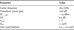
Table 4 compares the presented receiver front-end to the state of the art. It contains published front-ends of comparable levels of complexity. The third column shows which components, besides LNA and mixer(s), are included in each circuit.
Table 4. CMOS receiver front-ends of comparable complexity found in literature.

*Active chip area only (without pads).
The front-ends achieving the best performance for each column are highlighted. The comparison shows that the first strength of the proposed implementation is its very low power consumption of only 43 mW (which is even lower, i.e. 29 mW, without the baseband buffers). This value is lower than that of other receiver front-ends of comparable complexity. The second strength is the very small size of the presented implementation, which originates from the use of spiral inductors and the realization in 65 nm CMOS technology. Furthermore, the achieved conversion gain of 30 dB compares very favorable to the state of the art. The measured noise figure value indicates that the circuit also achieves good noise performance.
Regarding the realized bandwidth, the table shows that most of the receiver front-ends only cover parts of the unlicensed 60 GHz band. The proposed realization is no exception. With 5 GHz it exhibits a typical performance in this regard. The weak point with respect to the state of the art of the presented front-end is its linearity, quantified by an input-referred compression point of only −36 dBm. This low value can be explained by the front-end's low supply voltage of 1.0 V and its high conversion gain, which results in a saturation of the output stages. However, for the application of the front-end this is not critical, as the received input power is not expected to ever attain this compression point. An important point in low-power 60 GHz receiver design is to correctly predict the expected maximum input signal (usually originating from interference) and adjust the required linearity accordingly, as it is directly related to the achievable minimum power consumption.
VI. CONCLUSION
This paper presented the design and implementation of a low-power low-cost receiver front-end for the unlicensed 60 GHz band in 65 nm CMOS technology. With its very low power consumption of only 43 mW (further decreasing to 29 mW without the baseband buffers that are used to drive 50 Ω loads and are not necessary if a high-impedance integrated baseband circuit is employed), its extremely small circuit size of 0.55 mm2, its RF bandwidth extending from 56.5 to 61.5 GHz, and its very high conversion gain of 30 dB, the overall performance of the presented receiver front-end exceeds the state-of-the art.
This paper shows that to achieve this kind of results, the design of the 60 GHz building blocks must be optimized with respect to efficiency and both DC and LO power consumption (the latter in the case of the mixers). Furthermore, the interfaces between the blocks need not only to be power matched to each other, but also the power levels at these interfaces need to be accounted for to optimize overall system performance. Furthermore, the use of spiral inductors, rather than distributed elements, is essential for achieving small circuit size.
ACKNOWLEDGEMENTS
This work has been supported by the French National Research Agency (ANR) in the framework of the program Recherche Technologique Nano-INNOV/RT NANOCOMM project NANR-09-NIRT-004 and by the european Medea+ project QStream.
 Michael Kraemer was born in Bad Mergentheim, Germany, in 1980. He received the Dipl.-Ing. (BA) degree from BA Mosbach, Germany, in 2003 and the Dipl.-Ing. degree from the University of Stuttgart, Germany, in 2007, both in electrical engineering. During his studies, he stayed 1 year at University of Massachusetts, Amherst, USA, and did internships at ebm-papst GmbH, DaimlerChrysler AG and Robert Bosch GmbH. His research interests include the design and modeling of millimeter-wave circuits. The presented work was part of his doctoral studies at LAAS-CNRS in Toulouse, France, where he obtained the doctoral degree in December 2010. He is currently with the Collège des Ingénieurs in Paris, France. Dr. Kraemer is a Fulbright fellow and the recipient of the 2007 VDE-award at the University of Stuttgart.
 Daniela Dragomirescu was born in Bucharest, Romania in 1972. She received the Electronics and Telecommunication engineering degree from Bucharest Polytechnic University, Romania in 1996 and her Ph.D. degree from the National Institute of Applied Sciences, Toulouse, France. She is an Associate Professor at National Institute of Applied Sciences, Toulouse and a researcher at Laboratory for Analysis and Systems' Architecture (LAAS-CNRS). Her main research interests are in wireless sensor networks, system architecture and modeling, and digital and RF circuit design.
 Robert Plana was born on March 1964 In Toulouse. He obtained his Ph.D. in 1993 at LAAS-CNRS and Paul Sabatier University on the noise modelling and characterization of advanced microwave devices (HEMT, PHEMT, and HBT) that includes the reliability. In 1993, as associate professor at LAAS-CNRS, he has started a new research area concerning the investigation of millimeter-wave capabilities of silicon based technologies. More precisely, he has focused on the microwave and millimeter-wave properties of SiGe devices and their capabilities for low-noise circuits. In 1995, he has started a new project concerning the improvement of the passives on silicon through the use of MEMS technologies. In 1999, he has been involved with SiGe semi-conductor in Ottawa where he was working on the low-power and low-noise integrated circuits for RF applications. In the same year, he has received a special award from CNRS for his works on silicon-based technologies for millimeter-wave communications. In 2000, he has been professor at Paul Sabatier University and Institut Universitaire de France and he has started a research team at LAAS-CNRS in the field of micro and nanosystem for RF and millimeter-wave communications. Its main interests are on the technology, design, modeling, test, characterization, and reliability of RF MEMS for low-noise and high-power millimeter-wave applications and the development of the MEMS IC concept for smart microsystems. He has built a network of excellence in Europe in this field “AMICOM” regrouping 25 research groups. He has authored and co-authored more than 300 international journals and conferences. In 2004, he has been appointed as Deputy Director of the Information and Communication Department at the CNRS Headquarter. From January 2005 to January 2006, he has been appointed director of the Information and Communication Department at CNRS. Since 2006, he is heading a research group at LAAS-CNRS in the field of micro and nanosystems for wireless communications. From November 2007 to November 2009, he joined the “French research Agency” where he is the project officer of the National Nanotechnology Initiative. Since November 2009, he is appointed as head of the department “Physic, Mathematics, Nanosciences & Nanotechnology, Information and Communication Technology” at the Ministry of research in charge of defining the French strategic for research and innovation.