


Introduction
The 5G frequency band has become a prominent band for the next-generation communication [Reference Muirhead, Imran and Arshad1]. It provides a high data rate, more capacity, very low latency, and a better quality of service. To overcome the issues of 4G communications which are high propagation loss, less bandwidth, and low gain the need arises to employ a 5G communication band further giving space to researchers to design antennas for 5G communication. There are various requirements to employ 5G technology such as low latency of <1 ms, mobility should be greater than or equal to 500 km/h, data rate from 2 to 20 Gbps, connection density of 1 million/km2, spectrum efficiency up to 9 bit/s/Hz, and importantly it should operate in the millimeter-wave frequency range [2, Reference Kumar, Dixit, Malekar, Raut and Shevada3]. Out of so many proposed antennas by researchers, the antipodal antenna is one of the best candidates for a 5G antenna as it can operate over a high-frequency range and at high gain [Reference Zhu, Liu and Wen4, Reference Kumar and Dixit5]. Dr. Gibson invented the Vivaldi antenna in 1979 [Reference Gibson6] and later in 1988 Dr. Gazit modified Vivaldi to antipodal Vivaldi antenna (AVA) [Reference Gazit7]. The AVA was designed to operate at a very high and wide frequency band. As a single-patch AVA cannot meet the specifications of 5G antennas, the AVA array needs to be designed [Reference Yao, Cheng, Wang, Yu and Chen8]. In [Reference Kumar and Dixit9], the importance of AVA, its advantages, and applications are explained in detail.
The AVA array has some issues such as more side-lobe levels which affect the front-to-back ratio and high mutual coupling that affects antenna gain [Reference Dixit, Kumar, Urooj and Malibari10]. For the improvement of gain, low return loss, wide bandwidth, and stable radiation pattern AVA with performance enhancement techniques can be designed [Reference Dixit and Kumar11]. For the improvement in gain, researchers have incorporated various performance enhancement techniques such as slots [Reference Hokmabadi, Keshtkar, Bayat and Keshtkar12, Reference Mahmud, Islam, Rahman, Alam and Samsuzzaman13], corrugation [Reference Moosazadeh, Kharkovsky, Case and Samali14, Reference Zhu, Gao, Ho, See, Abd-Alhameed, Li and Xu15], multiple-input multiple-output (MIMO) [Reference Gupta, Briqech, Sebak and Ahmed Denidni16], array [Reference Guo and Qiang17], parasitic patch [Reference Nassar and Weller18, Reference Gao, Li, Zhang and Guo19], balanced AVA [Reference Juan, Guang, Lin and Demin20, Reference Sarkar, Saha, Shaik, Siddiqui and Antar21], metamaterial [Reference Li, Zhou, Gao, Wang and Lv22, Reference Pandit, Mohan and Ray23], substrate integrated waveguide (SIW) [Reference Ma and Feng24], and dielectric lens (DL) [Reference Moosazadeh and Kharkovsky25].
MIMO antennas suffer from a mutual coupling effect. The mutual coupling becomes stronger for a compact antenna. The reduction of mutual coupling is a daunting task [Reference Dixit, Shevada, Raut, Malekar and Kumar26]. Also, as the MIMO antenna consumes more power, most of the researchers design the AVA array. When single AVA is compared with an AVA array, the required parameters show better improvement. The array structure is mainly used to enhance the gain as proved in [Reference Liu, Yang, Zhang, Zhu, Wang and Huang27] where a single AVA patch provides 9 dBi gain and 1 × 8 AVA array provides 12.9 dBi gain. In [Reference Dixit and Kumar28], 1 × 4 AVA array is designed to achieve the gain of about 8.47–12.63 dBi, then the corrugations are implemented in array structure and gain has been improved to 8.2–13.2 dBi. In [Reference Dixit and Kumar29], the single-patch AVA with metamaterial and corrugations are designed on the FR4 substrate to achieve moderate gain and a cheaper antenna for 5G applications. Furthermore, the antenna gain can be enhanced by using a DL. A very high gain of about 23 dBi is obtained in [Reference Tiwari and Rama Rao30] after incorporating a rectangular DL in a 1 × 4 AVA array. Also, instead of a single layer of the DL, a multi-layer DL (each layer with different permittivity) can be added to AVA to enhance the gain [Reference Huang, Yang, Wu, Zhao and Liu31]. High gain can be achieved in low frequency by using two methods which are gradual corrugated edges as well as the triangular metal directors [Reference Zhu, Liu, Chen and Wen32].
The balanced AVA consists of three layers: the top and bottom layers function as ground and the middle layer functions as a conductor. This structure provides equal electric field distribution with respect to the ground but, the antenna design is complex. Similarly, the design of the metamaterial unit cell is also complex [Reference Dixit and Kumar33]. Furthermore, according to the literature survey, the DL enhances the gain more as compared to the parasitic patch. Hence, in this proposed antenna we have not used balanced AVA, metamaterial, and parasitic patch enhancement techniques.
In this paper, a 1 × 4 AVA array by incorporating corrugation and dielectric lens (AVA-ACDL) is proposed. The proposed antenna is simulated in software Ansys HFSS (version 19). The single-patch AVA with corrugations and dielectric lens (AVA-CDL) design is examined in Section “AVA-CDL design.” Next, the 1 × 4 AVA array with corrugations and dielectric lens (AVA-ACDL) design is elaborated in Section “AVA-ACDL design.” “Results” section expresses the measured and simulated results of the designed antenna and comparison of the proposed AVA-ACDL with AVAs available in the literature. Finally, the research paper is concluded in Section “Conclusion.”
AVA-CDL design
At first, the single AVA antenna is designed on the Rogers RO 4003C substrate having relative permittivity 3.55 as shown in Fig. 1. In Fig. 1, the top patch acts as a radiator and the bottom patch which is the mirror image of the top patch acts as a ground. The dimensions of single-patch AVA are 50 × 24.1 × 0.8 mm3. The single-patch AVA is connected with the 50 Ω microstrip transmission line. The elongated shaped slots are designed with the following exponential equations (1) and (2):

Fig. 1. Design of conventional AVA.
Outer curve equation Y 1 is:

Inner curve equation Y 2 is:

The length of antenna should be 3λ ≤ L ≥ 8λ and the antenna width should be nearly half the antenna length. Hence an optimum value of length (L) is selected as 50 mm and the optimized value of width (W) is 24.1 mm.
Next, corrugations are incorporated on both AVA patches as shown in Fig. 2. The corrugations are uniform and the same shape of metal cutting is present on the radiating patches. It helps to reduce the side and back lobes. Corrugation changes the inductance and capacitance of an antenna which in turn changes its frequency response and it helps in impedance matching. Here, the length and width of slots are optimized by the optimetrics tool of HFSS, and the corresponding reflection coefficients results are shown in Fig. 3 which shows that the optimum width of corrugation is 0.5 mm, and the optimum length of corrugation is 1.5 mm. Figure 4 depicts the current distribution at 29 GHz of a single patch with and without corrugations. Figure 4 proves the importance of corrugations in increasing the electrical length to boost the current density on the flat edges of patches which results in gain enhancement.

Fig. 2. Design of single-patch AVA with corrugations.
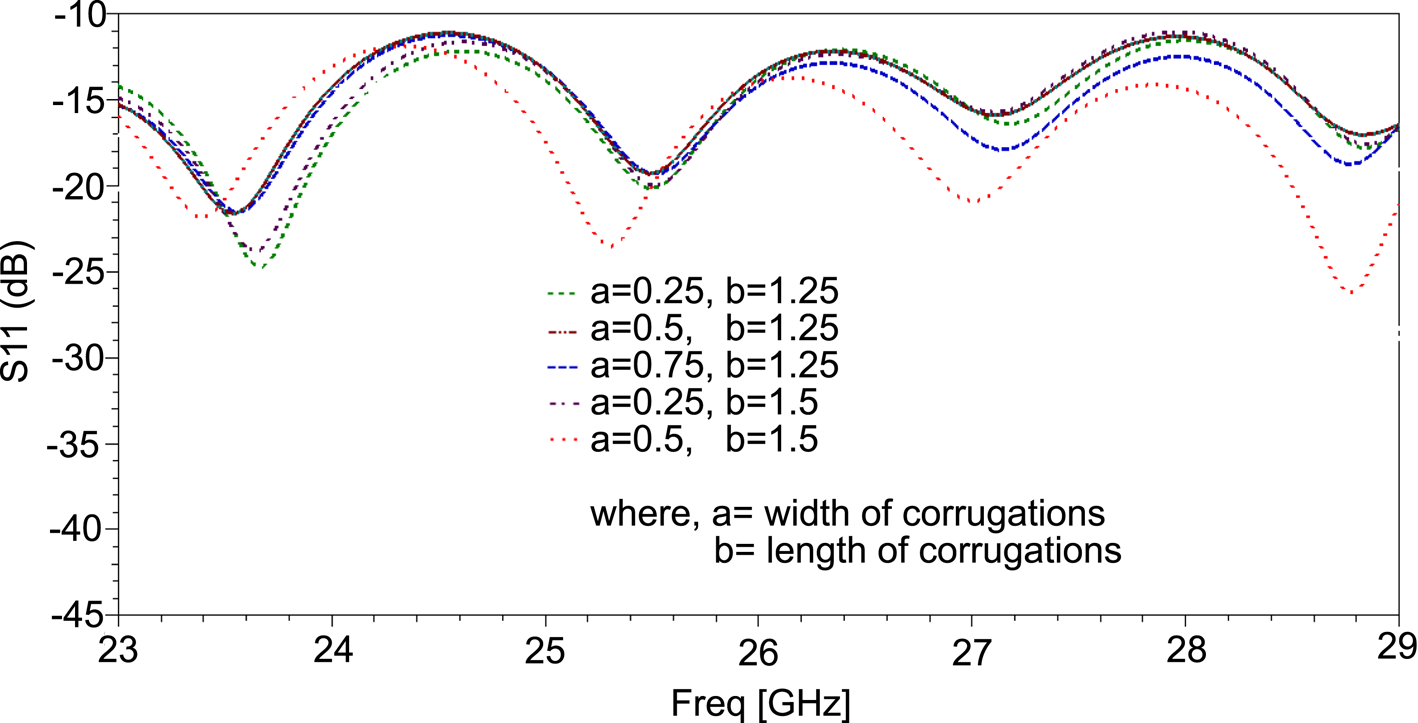
Fig. 3. S 11 of single-patch AVA with corrugations for different dimensions.

Fig. 4. Current distribution at 29 GHz.
Furthermore, the improvement in gain is done by incorporating the DL after the end of patches as shown in Fig. 5. The DL acts as a guide structure to produce a more directed radiation pattern. The DL uses substrate material. As seen in the recent literature, most of the researchers employ a trapezoidal-shaped DL as it enhances the gain more effectively [Reference Li, Zhou, Gao, Wang and Lv22]. This gain enhancement is also proved in Fig. 6. In Fig. 6, conventional AVA (CAVA) provides the lowest gain whereas AVA with corrugations enhances the gain more effectively. Further gain improvement is achieved after incorporating a DL which provides a gain in the range of 2.12–9.8 dBi. The dimensions of AVA-CDL are given in Table 1.

Fig. 5. Single-patch AVA-CDL.

Fig. 6. Gain versus frequency plot.
Table 1. Size of AVA-CDL

AVA-ACDL design
The 1 × 4 AVA-ACDL array with a feeding network, corrugations, and the DL is shown in Fig. 7. The size of the antenna is 97.2 × 71.2 × 0.8 mm3. The proposed 1 × 4 AVA array is designed and simulated in HFSS version 19. The impedance of the feeding network should match with the input impedance of the 50 Ω SubMiniature version A connector. The feeding network is designed by designing 50 Ω microstrip feed line at first. Then this path is divided into two paths of 100 Ω impedance microstrip feed line. This process is repeated to obtain four feeding paths to feed four antenna elements. After multiple iterations on HFSS, the dimensions of the feeding network are finalized. As shown in Fig. 8, the magnitude of the input impedance of 1 × 4 AVA-ACDL is very close to 50 Ω in the operating frequency range of 24.66–25 and 27.05–29 GHz.
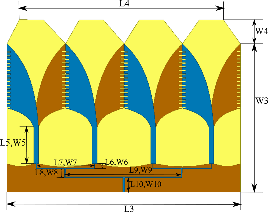
Fig. 7. 1 × 4 AVA array (AVA-ACDL).
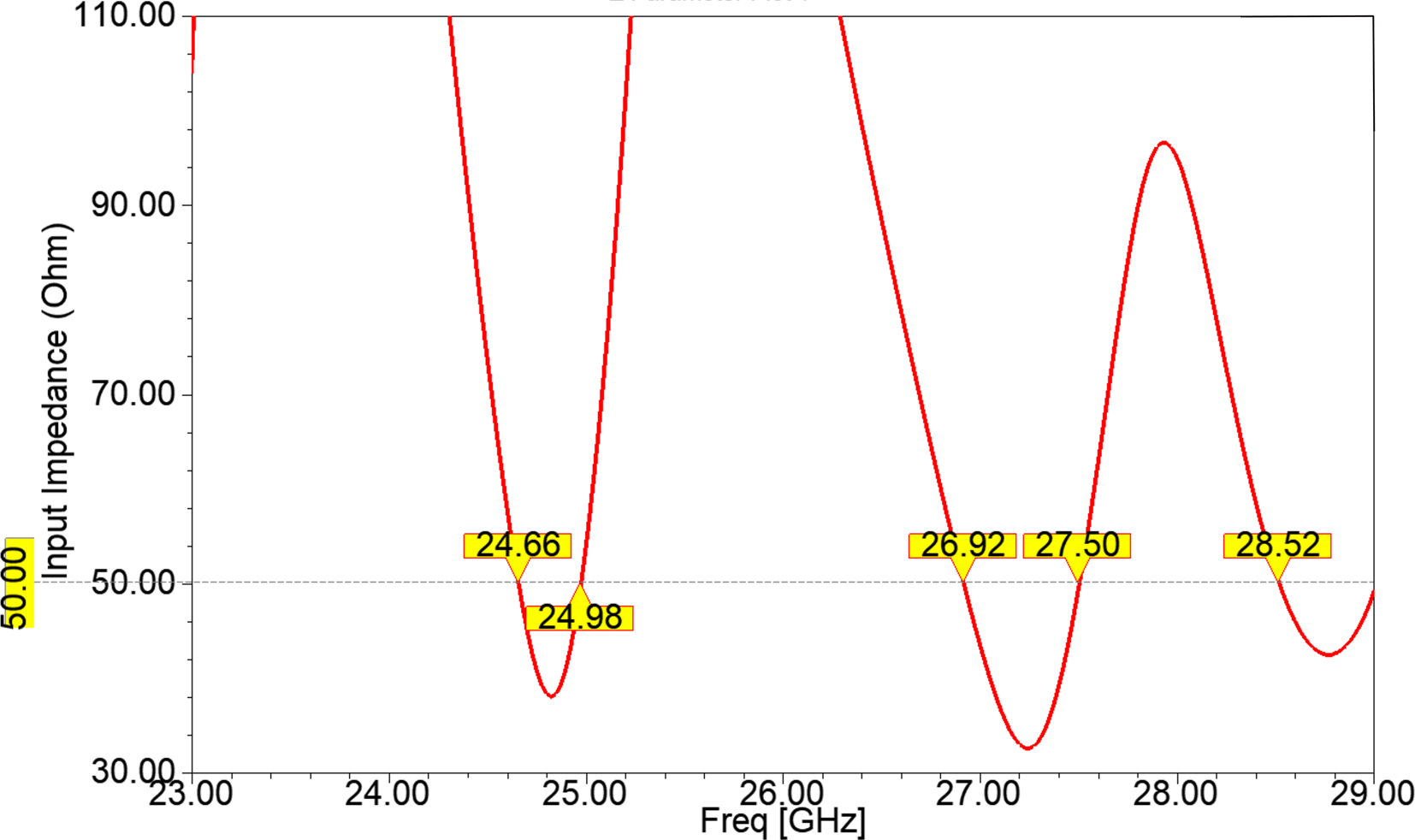
Fig. 8. Input impedance of AVA-ACDL.
As demonstrated in Fig. 9, the array structure helps to maximize electric held radiation at 29 GHz in the desired direction which results in gain enhancement. Also, from Fig. 9, it can be seen that the feeding network is designed to provide maximum and equal inputs to all four radiating AVA patches. Figures 10(a) and 10(b) show the top and bottom views of the fabricated antenna, respectively. The dimensions of AVA-ACDL are given in Table 2.

Fig. 9. Electric field distribution of AVA-ACDL at 29 GHz.

Fig. 10. Fabricated AVA-ACDL: (a) top patch and (b) bottom patch.
Table 2. Dimensions of the AVA-ACDL

Results
The proposed AVA-ACDL antenna is fabricated on the R04003C substrate. After fabrication, it is tested by using the N5224A performance network analyzer (PNA). The simulated and measured S 11 results of AVA-ACDL are shown in Fig. 11 which proves that both results are nearly the same. Initially, the PNA was calibrated to operate over 23–29 GHz frequency range and then S 11 of the fabricated antenna is tested. There is a minor difference between measured and simulated results due to antenna fabrication error. The simulated S 11 result shows that the antenna can be operated over dual frequency bands which are 24.66–25 GHz and 27.11–29 GHz. Also, the measured S 11 graph depicts that the dual-band operating frequencies are 24.59–24.98 GHz and 27.06–29 GHz which covers frequency bands of 5G applications.
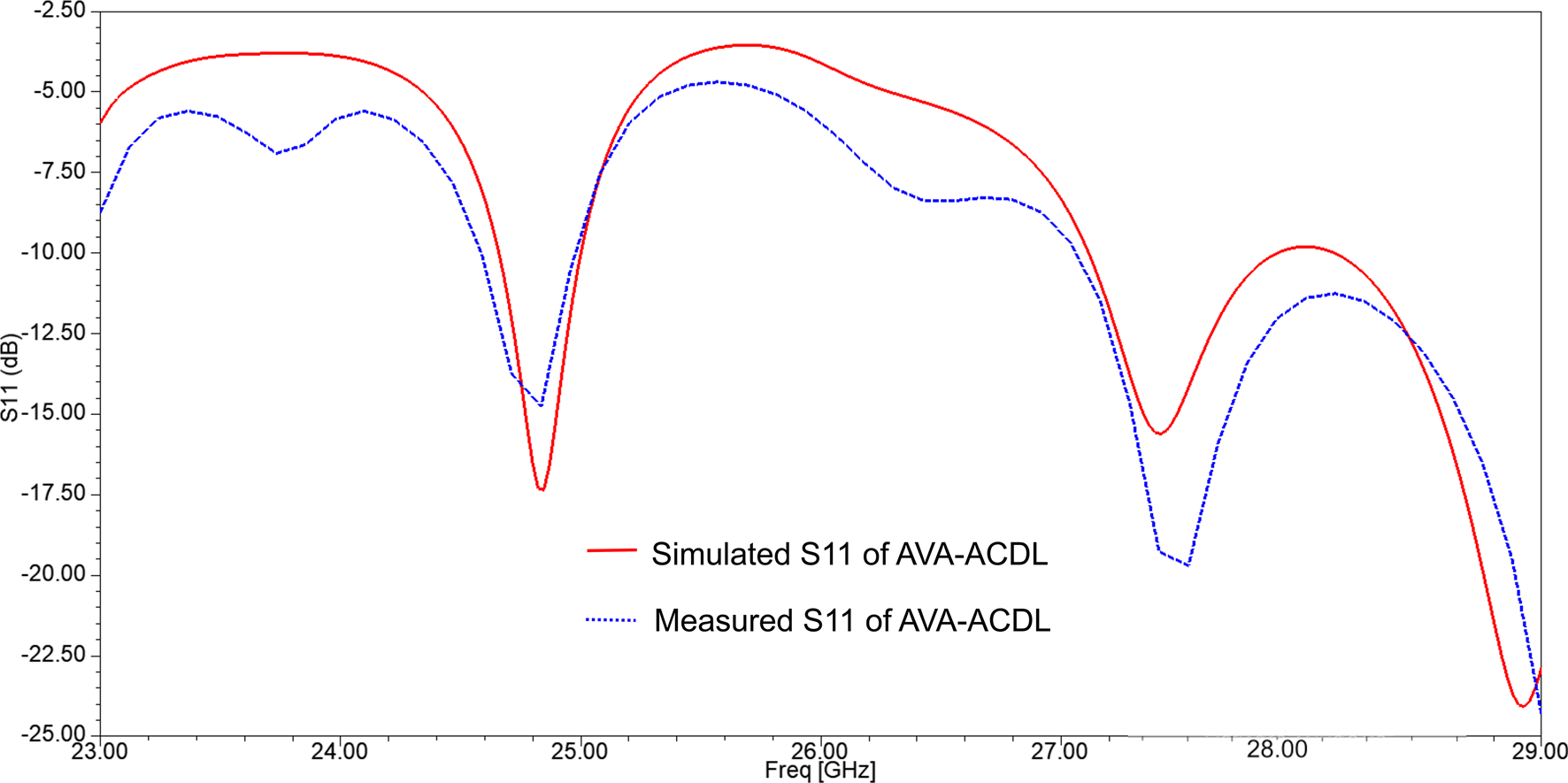
Fig. 11. Reflection coefficient of AVA-ACDL.
Next, the gain graph is plotted in Fig. 12. It proves that the proposed AVA-ACDL provides high and almost constant gain over the operating frequency range. The gain varies between 8 and 12 dBi. The maximum simulated gain is 12 dBi at 24.66 GHz whereas the maximum measured gain is 11.8 dBi at 29 GHz.
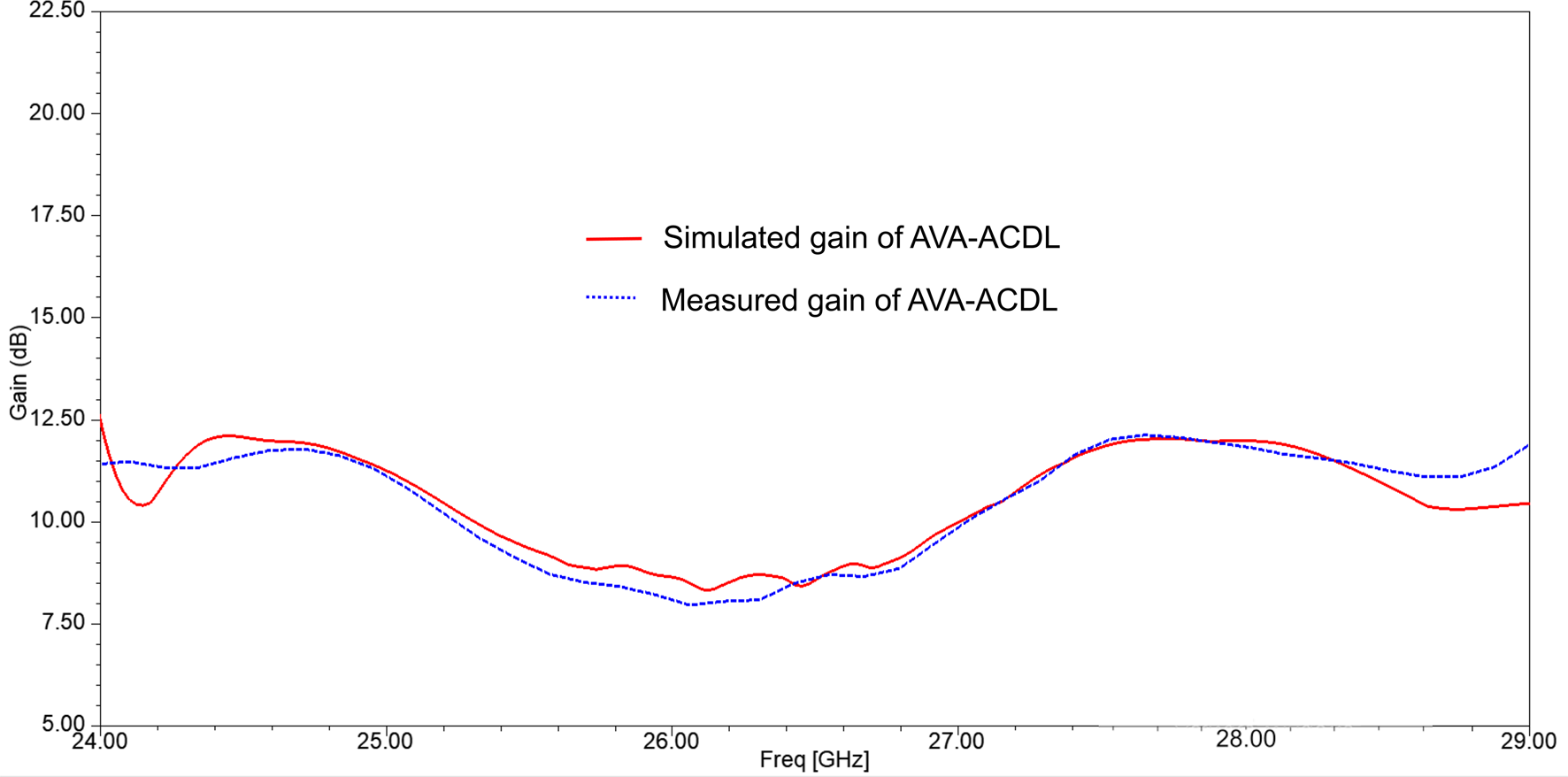
Fig. 12. Gain of AVA-ACDL.
Furthermore, the simulated and measured radiation patterns of AVA-ACDL at 24.7, 28.5, and 29 GHz are shown in Fig. 13. Figure 13(a)–(c) show E plane radiation patterns and Fig. 13(d)–(f) show H plane radiation patterns. It can be seen from Fig. 13 that the E and H plane radiation patterns are almost stable over the operating frequency range of an antenna. Also, the back and sidelobe levels are low due to corrugations and the enhanced gain is achieved as a combined effect of an array, corrugations, and DL.

Fig. 13. Radiation pattern of AVA-ACDL: (a–c) E plane and (d–f) H plane at 24.7, 28.5, and 29 GHz, respectively).
The comparison of the proposed AVA-ACDL with other AVA arrays available in the literature is presented in Table 3. The comparison is done based on the number of array elements, antenna size, gain, and frequency range. This table proves that the proposed antenna has used a smaller number of array elements as compared to others. Also, it provides the highest and almost constant gain as compared to others. In [Reference Liu, Yang, Zhang, Zhu, Wang and Huang27, Reference Zhu, Liu, Chen and Wen32] antenna size is moderate, but the gain variation is more. Next, in [Reference Horst, Ghasr and Zoughi34, Reference Osama M. Dardeer and Ashraf S. Mohra35] the gain of an antenna is very less. Hence, according to this comparison table, the proposed antenna is a very appropriate choice for integrating it in 5G communication devices.
Table 3. Comparison of the AVA-ACDL with AVA array from literature

Conclusion
In this paper, a dual-band, 1 × 4 AVA-ACDL array with DL and corrugations for 5G communications is presented. At first, the corrugations have been introduced on the radiating elements for increasing the front-to-back ratio. Furthermore, the DL is used for improvement in the gain. The proposed AVA-ACDL operates at a dual-band (24.59–24.98 GHz and 27.06–29 GHz) frequency range. The parametric analysis is done for the optimization of antenna parameters. The designed antenna has achieved a high and constant gain of 8–12 dBi over operating frequency. Also, the measured and simulated results are identical to each other. The proposed antenna has a further scope of improvement in bandwidth and size reduction by incorporating different performance enhancement techniques such as slots, SIW, and metamaterial. The proposed antenna provides a better gain and stable radiation pattern over the desired frequency range and makes it useful for 5G communication devices.
Acknowledgments
This study was supported by Symbiosis International (Deemed University) under Major Research Project (MJRP) grant.
 Sumit Kumar received his bachelor's degree in Electronics and Communication from Kurukshetra University, Kurukshetra, India in 2005, his master's degree from the Guru Jambheshwar University of Science and Technology, Haryana, India in 2008, and Ph.D. degree from Jamia Millia Islamia, Delhi, India in 2017. Currently, he is working as an Associate Professor at the Electronics and Telecommunication Department of Symbiosis Institute of Technology, Symbiosis International (Deemed University), Pune, Maharashtra, India. His research areas are antenna design, wireless networks, wireless communication, and computational intelligence.
 Amruta S. Dixit received her bachelor's degree in Electronics and Telecommunication from Pune University, Maharashtra, India in 2008 and her master's degree in Signal Processing from Pune University, Maharashtra, India in 2012. She is currently pursuing her Ph.D. at the Symbiosis Institute of Technology, Symbiosis International (Deemed University), Pune, Maharashtra, India. Currently, she is a Junior Research Fellow at Symbiosis International (Deemed University). Her research areas are the antenna design and 5G communication.


