I. INTRODUCTION
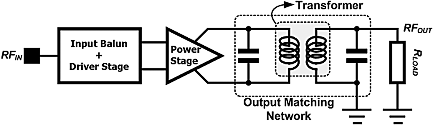
Recently, various RF CMOS power amplifiers have been introduced that boast lower costs and offer a greater possibility for integration with digital and analog circuits as compared to power amplifiers fabricated using a compound semiconductor [Reference Kim, Son, Kim and Park1–Reference Luque, Kerherve, Deltimple, Leyssenne and Belto12]. Unlike power amplifiers using a compound semiconductor, the CMOS power amplifier uses a differential structure to utilize the virtual ground [Reference Koo, Na and Hong13, Reference Chung, Kuo and Chiou14]. Accordingly, the input and output baluns in the CMOS power amplifier are essential for the RF front-end, where single-ended signals are used. In general, output baluns are designed using transformers. In the differential power amplifier, the parasitic components of the transformer can be utilized as the components of the output matching network, whereas the transformer itself acts as the output balun [Reference Aloui, Leite, Demirel, Plana, Belto and Kerherve15, Reference Joo, Lee, Shim and Hong16]. In a variety of previous works in which the transformer is used as an output balun, the output matching network has been completed with a transformer and two additional capacitors, as shown in Fig. 1. As depicted in Fig. 1, the output matching network can then be very simple if the transformer is used as the output balun. Based on the structure of a CMOS power amplifier using a transformer, as shown in Fig. 1, various modifications have been proposed [Reference Park, Kim, Kim and Hong17–Reference Park and Seo23]. Basic equivalents of the CMOS power amplifiers can be represented as shown in Fig. 1.

Fig. 1. Simple block diagram of a typical CMOS power amplifier using a transformer as an output balun.
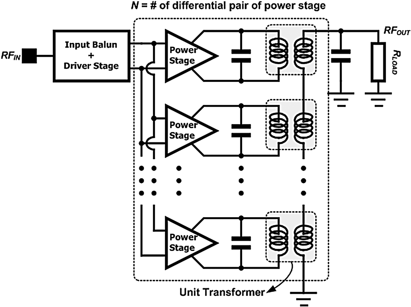
Additionally, a distributed active transformer (DAT) has been introduced to elevate the output power and efficiency of CMOS power amplifiers [Reference Aoki, Kee, Rutledge and Hajimiri7]. The DAT can be used as part of a power-combining method to maximize the performances of multiple differential pairs of power stages. Figure 2 shows a simplified structure of the power amplifier using a DAT.
Fig. 2. Simple block diagram of a typical CMOS power amplifier using a DAT.
In this study, we propose a design methodology for a switching-mode CMOS power amplifier in which the output transformer is utilized as the output balun. The proposed methodology takes into consideration the breakdown voltages and optimum size of the power transistor of the power stages. Additionally, a technique to determine the initial values of the capacitor and the parasitic inductance of the output transformer is included in the proposed methodology.
II. PROPOSED METHODOLOGY
Figure 3 shows a simplified schematic of the power stage and the output matching network of a switching-mode RF CMOS power amplifier using a transformer as an output balun. Although we draw the power stage using a simple common-source structure, the power stage can be designed using a cascode structure. Essentially, the transformer converts the differential signal into a single-ended signal. The output matching network is completed using the parasitic inductances of the transformer and two additional capacitors. In general, the load impedance, R L, of the power amplifier is designed to be 50 Ω.
Fig. 3. Simple schematic of the power stage of a typical CMOS power amplifier using a transformer as an output balun.
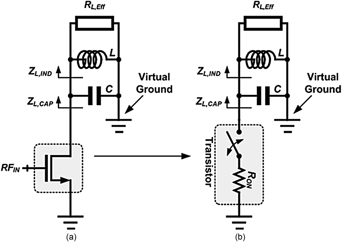
For the sake of simplicity of the analysis, we represent the schematic in Fig. 3 as an equivalent circuit using the half-circuit concept, as shown in Fig. 4(a). The capacitance, C F, connected between the drains of the differential transistors, is converted according to the formula C = 2C F, as shown in Fig. 4. Although the coupling factor k between the primary and the secondary parts of the transformer in Fig. 3 is always lower than one, we assume that the value of k is one to simplify the analysis. Hence, Z L,IND in Fig. 3 can then be expressed as a parallel connection between R L,EFF and L, where R L,EFF and L are the equivalent load impedance and the inductance of Z L,IND in Fig. 3, respectively [Reference Chang and Lin11]. If the turn ratio of the transformer is one with k = 1, R L,EFF and L in Fig. 4 become half of R L in Fig. 3 and the inductance of the primary part of the transformer, respectively. Additionally, given that the power amplifier operates in the switching mode, the transistor in Fig. 4(a) can be modeled as a switch with the on-resistance, R ON, of the transistor, as shown in Fig. 4(b). We summarize the assumptions made in the analysis of the proposed design methodology as follows:
(1) Coupling factor (k): 1;
(2) Turn ratio of the output transformer: 1.
Fig. 4. Simple block-diagram of a typical CMOS power amplifier using a transformer as an output balun.
A) Determination of N and R L,EFF
As depicted in Fig. 4, N is defined as the number of differential pairs of the power stage. The output power, P OUT, of the power amplifier can then be represented as follows:
 $$P_{OUT} = 2NP_{UNIT}. $$
Here, P UNIT is the power generated in each half-circuit of the power stages [Reference Park, Han, Kim and Hong22]. With the assumptions described above, the effective load resistance of each half-circuit and P UNIT are represented as follows:
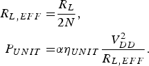 $$\eqalign{R_{L,EFF} = & \displaystyle{{R_L} \over {2N}}, \cr P_{UNIT} = & \alpha \eta _{UNIT} \displaystyle{{V_{DD}^2} \over {R_{L,EFF}}}.} $$
Here, α and η UNIT are the coefficients according to the type of amplifier and the efficiency of each half-circuit, respectively. For example, if the designed power amplifier is a class-E amplifier, then α is 0.577. The P OUT in equation (1) can then be obtained with the following equation:
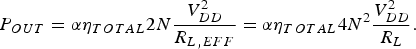 $$P_{OUT} = \alpha \eta _{TOTAL} 2N\displaystyle{{V_{DD}^2} \over {R_{L,EFF}}} = \alpha \eta _{TOTAL} 4N^2 \displaystyle{{V_{DD}^2} \over {R_L}}. $$
In this equation, η TOTAL is the overall drain efficiency of the power stage [Reference Park, Han, Kim and Hong22]. In general, R L is 50 Ω for a RF system. Thus, if the targets of the output power and drain efficiency are determined, N can then be determined as follows:
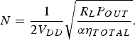 $$N = \displaystyle{1 \over {2V_{DD}}} \sqrt {\displaystyle{{R_L P_{OUT}} \over {\alpha \eta _{TOTAL}}}}. $$
With the determined value of N from equation (4) the desired values of P UNIT and R L,EFF can easily be calculated using equation (2).
B) Determination of the transistor size
Generally, the on-resistance R ON is designed to be much smaller than the R L,EFF value for high efficiency at the maximum output power of the power amplifier. The relationship between R ON and R L,EFF can then be defined as
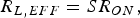 $$R_{L,EFF} = SR_{ON}, $$
where ‘S’ is the proportional constant for R L,EFF and R ON. For example, S is designed to be higher than ten for a general power amplifier to maximize the drain efficiency at the maximum output power.
C) Determination of the inductance L and the capacitance C
With the assumptions described above, the inductance L and capacitance C are determined by the operating frequency and breakdown voltage of the transistor used. The operating frequency f can then be defined as
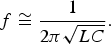 $$f \cong \displaystyle{1 \over {2\pi \sqrt {LC}}}. $$
Additionally, because the peak energy stored in the inductor is identical to that in the capacitor, the relationship between the peak current i peak through L and the peak voltage V peak across C can then be described as
 $$\eqalign{\displaystyle{1 \over 2}Li_{peak}^2 & = \displaystyle{1 \over 2}Cv_{peak}^2 \,\,\,\, \to \,\,\,\,v_{peak} \cr & = \displaystyle{1 \over {2\pi \hskip1ptf}}\displaystyle{{i_{peak}} \over C} = 2\pi \hskip1ptfLi_{peak}.} $$
The current, i(t), through L can be represented as follows:
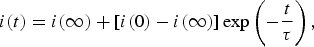 $$i(t) = i(\infty ) + \left[ {i(0) - i(\infty )} \right]\exp \left( { - \displaystyle{t \over \tau}} \right),$$
 $$\tau = \displaystyle{L \over {R_{ON} //R_{L,EFF}}} \cong \displaystyle{L \over {R_{ON}}}, $$
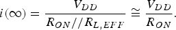 $$i(\infty ) = \displaystyle{{V_{DD}} \over {R_{ON} //R_{L{\rm,} EFF}}} \cong \displaystyle{{V_{DD}} \over {R_{ON}}}. $$
Here, τ is a time constant. In equations (9) and (10), R ON // R L,EFF is approximated as R ON given that R ON is at least ten times smaller than R L,EFF. In equation (10), we assume that i(0) is zero; the phase of the resonant current in the LC resonant circuit is zero at t = 0. Accordingly, the peak current i peak appears at t = 0.25T, where T is the period. The i peak value can then be calculated as
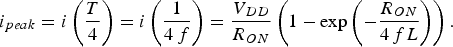 $$i_{peak} = i\left( {\displaystyle{T \over 4}} \right) = i\left( {\displaystyle{1 \over {4\,f}}} \right) = \displaystyle{{V_{DD}} \over {R_{ON}}} \left( {1 - \exp \left( { - \displaystyle{{R_{ON}} \over {4\,fL}}} \right)} \right).$$
From equations (7) and (11), the peak voltage v peak across the capacitor is calculated as
 $$v_{peak} = 2\pi \hskip1ptfL\displaystyle{{V_{DD}} \over {R_{ON}}} \left( {1 - \exp \left( { - \displaystyle{{R_{ON}} \over {4fL}}} \right)} \right).$$
To remove the reliability problem, the inductance L is designed for v peak to be lower than the breakdown voltage of the transistor. After determining L, the capacitance C can be determined using equation (6).
III. DESIGN EXAMPLE: A 2.4-GHZ SWITCHING-MODE CMOS POWER AMPLIFIER
To verify the feasibility of the proposed design methodology, we design a 2.4-GHz switching-mode CMOS power amplifier as a design example. The amplifier is fabricated using 0.18-μm RF CMOS technology. Spiral transformers are used as the input and output baluns. The cascode structure is adapted to moderate the low breakdown voltage problem associated with CMOS.
A) Determination of the key design parameters through the proposed design methodology
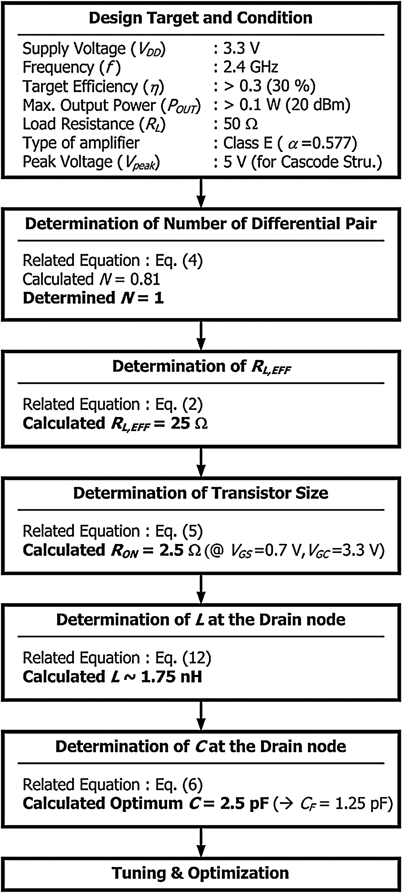
Figure 5 shows the design flow of the power amplifier, which is designed as an example using the proposed design methodology. First, the designed target and conditions are checked to determine the design parameters of the amplifier, as shown in the first step of Fig. 5. From the design targets and conditions, we determine the number, N, of differential pairs of the power stage. Although the calculated N is 0.81 from equation (4), we determine N to be 1 given that it must be an integer. With an N of 1, R L,EFF of equation (5) is approximately 25 Ω. R ON must then be designed to be lower than 2.5 Ω. The values of L and C are determined incrementally, as shown in Fig. 5.
Fig. 5. Design flow chart using the proposed methodology.
We design the power amplifier with the determined key design parameters shown in Fig. 5. Given that we use a cascode structure in the power stage, R ON needs to include the on-resistances of the common-source (M CS) and common-gate (M CG) transistors. In this study, the gate bias of M CG is 3.3 V (=V DD). If the peak voltage at the gate of the M CS reaches 3.3 V, R ON can be calculated with a common-source transistor gate voltage of 3.3 V. Figure 6(a) shows the simulated R ON of the designed power stage. The gate lengths of M CS and M CG are 0.18 µm and 0.35 µm, respectively. The total gate widths of M CS and M CG are designed for R ON to be nearly 2.5 Ω, as shown in Fig. 6(a).
Fig. 6. Simulation results to determine the design parameters: (a) on-resistance, R ON, of the power stage; (b) peak voltages, V peak, according to the R ON and L; and (c) inductance, L, of the primary part of the transformer.
Figure 6(b) shows the calculated value of V peak at the drain node of the cascode according to R ON and L. As shown in Fig. 6(b), the proper value of L is approximately 1.75 nH with a previously determined R ON of 2.5 Ω. Although we can choose a value of L higher than 1.75 nH, the loss increases as the required inductance is increased. Thus, we design the primary part of the output transformer to be around 1.75 nH. Figure 6(c) shows the simulated inductance, L, of the primary part of the designed output transformer. To obtain the desired inductance of the primary part, we vary the length and width of the metal lines of the transformer. The parasitic components, mutual inductance, and load impedance are included in the simulated inductance, L, shown in Fig. 6(c).
B) Design of the fully integrated 2.4-GHz power amplifier
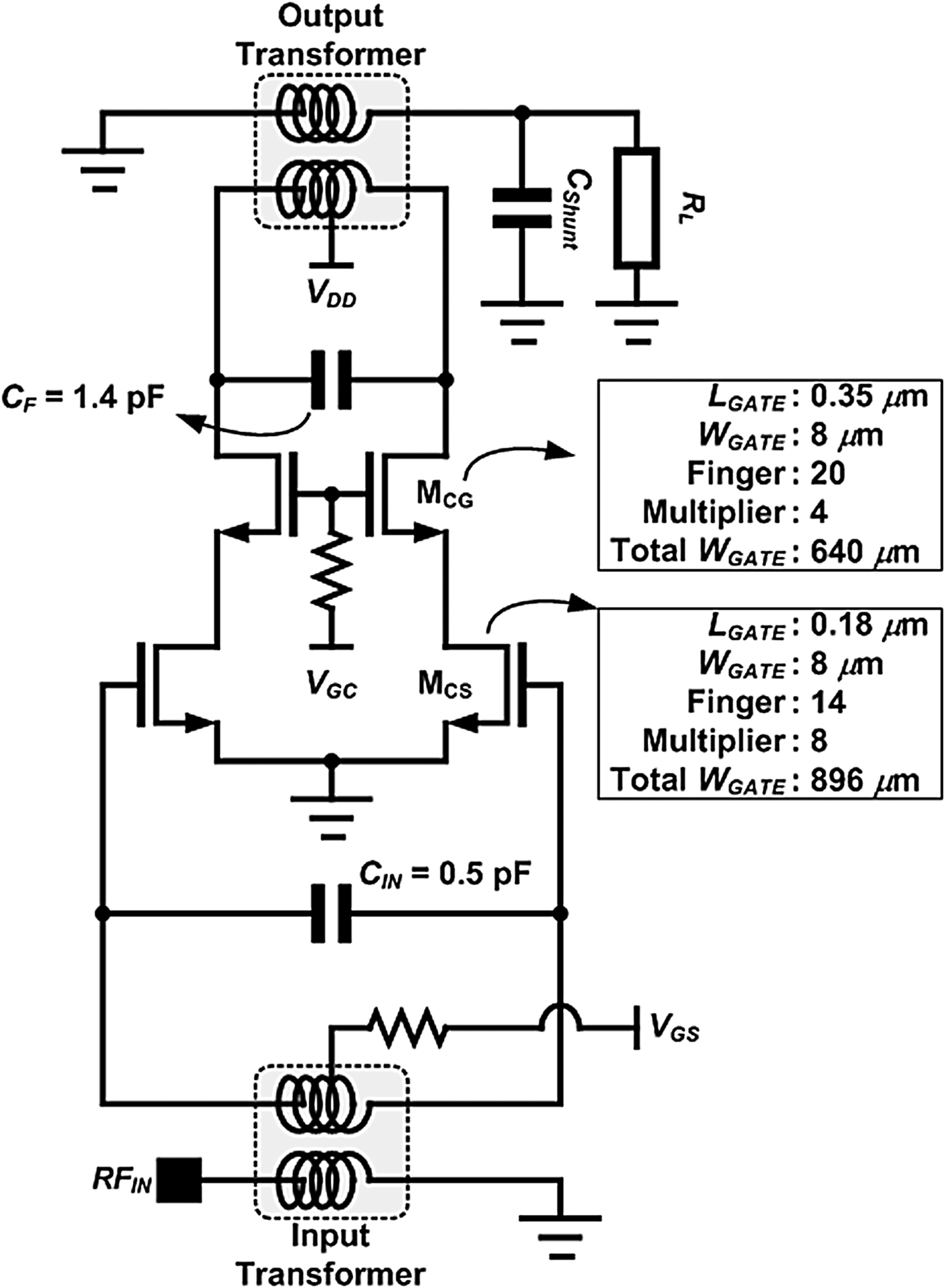
Figure 7 shows a schematic of the designed power amplifier using the proposed design methodology. Although the initial values of the key design parameters are determined using the proposed design methodology, additional tuning and optimization steps are required because the methodology includes the assumptions described in Section II. For example, although the calculated C F from Fig. 5 is 1.25 pF, ultimately the value of C F used is 1.4 pF as a result of the optimization of the amplifier. In this work, an additional MIM capacitor for C Shunt is not used because the parasitic capacitance of the designed output transformer is sufficient for C Shunt.
Fig. 7. Design example: schematic of the designed power amplifier using the proposed design methodology.
C) Measurement results
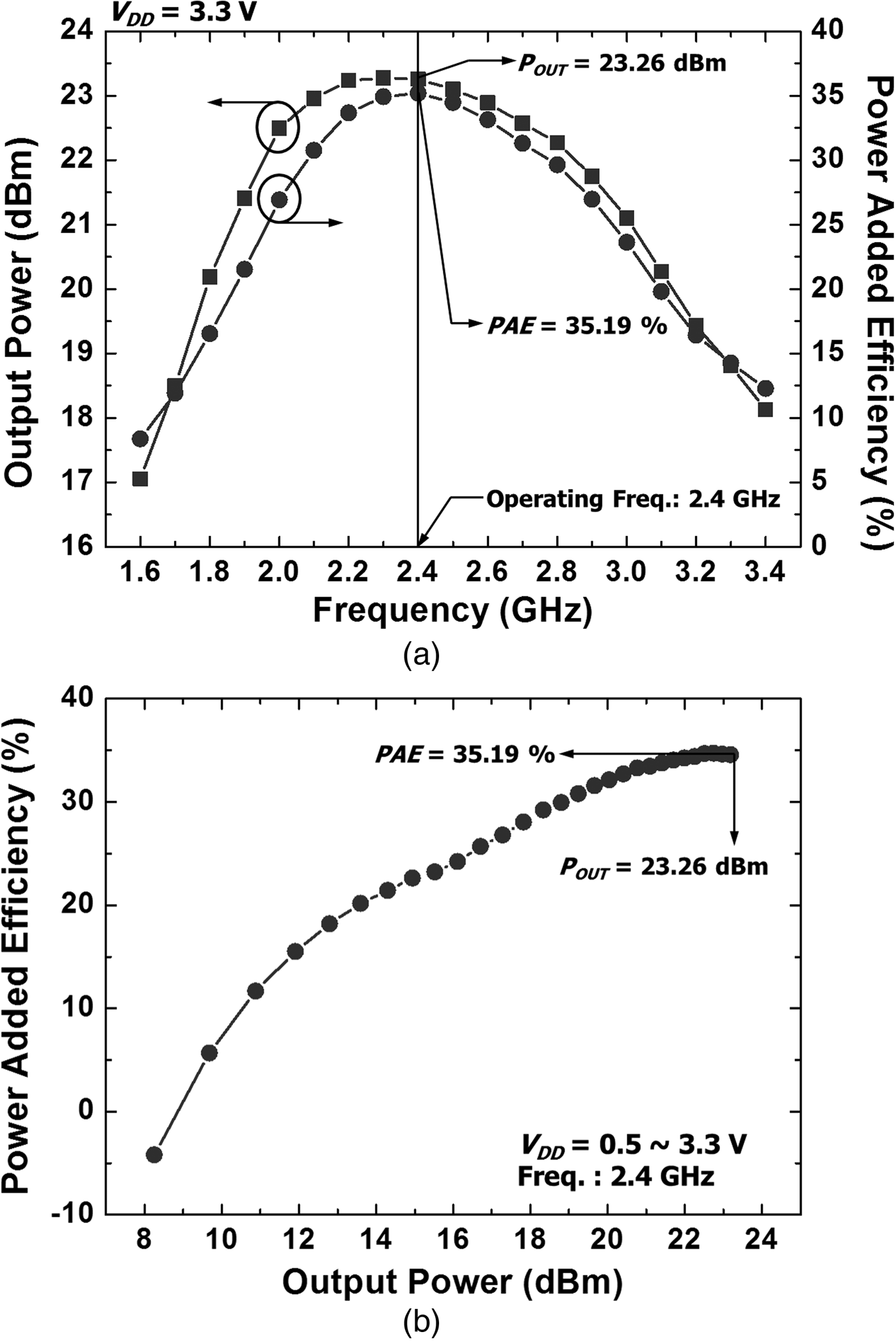
Figure 8 shows a chip photograph of the designed power amplifier. The chip size is 1.4 × 0.6 mm2. All of the input and output matching networks, transformers, and test pads are fully integrated. Figure 9(a) shows the measured output power and power-added efficiency (PAE) according to the operating frequency with a fixed supply voltage, V DD, of 3.3 V. Although we used the drain efficiency in the theoretical analysis, the PAE is used in the measured results. Given that the PAE includes the effects of the input power in the calculation of the efficiency, the PAE is more popularly used when comparing the efficiencies of various power amplifiers as compared to the drain efficiency. Moreover, the PAE value is slightly lower than that of the drain efficiency. As provided in Fig. 9(a), the output power and PAE at 2.4 GHz are 23.26 dBm and 35.19%, respectively. Given that the value of N used is higher than the calculated N of 0.81, we obtain higher output power and a higher PAE value relative to the target values. Figure 9(b) shows the PAE versus the output power when V DD ranges from 0.5 to 3.3 V.
Fig. 8. Photograph of the designed power amplifier.
Fig. 9. Measured results: (a) output power and efficiency according to the operating frequency and (b) efficiency versus output power.
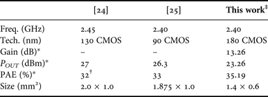
Additionally, the degradation of the output power with time is measured to check the robustness against changes in the temperature. With continuous-wave input power, the output power is degraded by approximately 0.1 dB over a time of 60 min. Table 1 summarizes the measurement results and compares them with previously reported results with a 2.4 GHz switching-mode power amplifier.
Table 1. Comparison of switching-mode CMOS power amplifiers.
* In the saturation condition.
† Drain efficiency.
‡ Single stage.
IV. CONCLUSION
In this study, we proposed a design methodology for a switching-mode RF CMOS power amplifier to obtain the initial values of key design parameters in the first step of the design of the amplifier. The methodology considers the peak voltage of the drain node of the amplifier as well as the number of differential pairs of the power stages. Although additional tuning is required after the determination of the key design parameters through the methodology, the methodology successfully provides reasonable initial values of the parameters. From the design example of a power amplifier, the feasibility of the proposed methodology is proved.
ACKNOWLEDGEMENTS
This work was supported through a grant from the Human Resources Development program (No. 20124010203160) of the Korea Institute of Energy Technology Evaluation and Planning (KETEP) funded by the Ministry of Trade, Industry, and Energy of the Korean government.
Changhyun Lee received his B.S. and M.S. degrees in Electronic Engineering from Soongsil University, Seoul, in 2011 and 2013, respectively, and is currently working toward a Ph.D. at Soongsil University. His current research interests include CMOS RF power amplifiers and transceivers for wireless chip-to-chip communication.
Changkun Park received his B.S., M.S., and Ph.D. degrees in Electrical Engineering from Korea Advanced Institute of Science and Technology (KAIST), Daejeon, Korea, in 2001, 2003, and 2007, respectively. From 2007 to 2009, he was with the Advanced Design Team of the DRAM Development Division, Hynix Semiconductor Inc., Icheon, Korea, where he was involved in development of high-speed I/O interfaces of DRAM. In September of 2009, he joined the faculty of the School of Electronic Engineering, Soongsil University, Seoul, Korea. His research interests include RF and millimeter-wave circuits, RF CMOS power amplifiers, and wireless chip-to-chip communication and power transfers.