Introduction
The rapid growing of the broadband wireless communication system leads to the enhancement of the information accessibility [Reference Ge, Esselle and Bird1]. Using polarization diversity to reduce the number and size of antennas is one of the promising approaches to increase the communication link capacity. In general, dual-polarized microstrip antennas are divided into two categories as single-port and double-port configurations. Single-port structures have more complex feeding mechanism in comparison to double-port ones with suboptimal performance from the impedance bandwidth point of view. However, single-port structures use only one port to excite both orthogonal polarizations and therefore the isolation factor is not discussed. A lot of studies have been carried out on dual-polarized planar and non-planar antennas for multiple-input–multiple-output and wireless local area network (WLAN) applications [Reference Gou, Yang, Li and Nie2–Reference Zheng, Zhang, Li and Leng7]. Using non-planar structures improves the overall performance of these antennas thanks to the design of various feeding mechanism which could lead to an increase in the isolation between ports. However, in most cases, these structures are not useful for array configurations because of complex feeding network and size limitation. Isolation between two ports, miniaturization, and impedance bandwidth are three main challenges in designing a broadband dual-polarized microstrip antenna [Reference Luo, Ding, Hu and Cao8]. Several techniques have been employed to achieve high isolation between two input ports and broaden the impedance bandwidth such as capacitive- and slot-coupled feed, L-probe feed, and two hybrid input port structures [Reference Wong, Lau and Luk9–Reference Chiou and Wong11]. By developing the multi-layer fabrication technology, the double-sided printed radiators etched on two sides of a substrate are of interest [Reference King and Chang12]. Almost, these antennas are composed of the dipole whose each arm is printed on one side of the substrate. This arrangement allows to reduce the substrate thickness and hence decreases the surface wave losses. Therefore, the unwanted radiations are suppressed and consequently the antenna radiation performance is enhanced [Reference Liu, Yi, Wang and Gong4, Reference Tefiku and Grimes13–Reference Huang and Liang15]. Employing the parasitic patches for gap-coupling to the main radiators is a well-known approach to enhance the frequency bandwidth of the microstrip antennas. The main advantage of adding parasitic patch is the enhancement of the frequency bandwidth while keeping the antenna dimensions and also electromagnetic properties of the main radiators [Reference Kandwal and Khah16]. In this paper, a broadband dual-layer dual-orthogonal polarized microstrip antenna is presented. The proposed antenna benefits from wideband radiators and wideband feeding mechanism for both polarizations. Using two radiating patches, including double-sided strip dipole and annular ring, in two separate layers, helps to achieve better isolation between two ports. Besides, by incorporating a diamond-shape parasitic patch at the top side of the upper substrate located at the center of the annular ring, impedance bandwidth of the strip dipole is greatly enhanced. Antenna configuration and simulation results are presented in “Antenna configuration and design methodology” section and experimental results are presented in “Experimental results and discussions” section. “Conclusion” section is dedicated to conclusions.
Antenna configuration and design methodology
Figure 1 depicts the configuration of the proposed dual-layer antenna along with the arrangement of two radiating patches. The antenna dimension is 57 mm × 67 mm × 73 mm, consisting of two separate dielectric layers which are made up of Taconic RF-35 with 0.762 mm thickness and ε r = 3.5. The separation between two dielectric layers is specified with h 0 parameter. As shown in Fig. 1, wideband double-sided strip dipole and annular ring configurations along with corresponding transition lines are etched on both sides of the lower and upper substrates, respectively. These two patches are arranged perpendicularly to each other enabling dual-orthogonal polarization. A ground plane with a given distance of λ/16 from the lower substrate with the same dimensions as the substrate has been added to decrease the back lobe of the radiation pattern and consequently enhance the overall gain at the broadside direction. The wavenumber λ corresponds to the frequency of 5.5 GHz. To accommodate two orthogonal polarizations, i.e., H-Pol and V-Pol, the radiation patches are fed through two wideband baluns connecting to the patches by two linearly smooth tapered transition lines (see Fig. 1). Since it is difficult to find the optimum values of all design parameters of the antenna to fulfill all desired factors such as S-parameters and the peak gain simultaneously, we carried out the design process in two steps. At the preliminary design step, by tuning the design parameters of the antenna without considering the parasitic patch, we attempted to find the best amount of return loss for H-pol mode along with high isolation between two ports in a wide frequency band around 5.5 GHz. In this step, the return loss from port #1 is not important in optimization. Afterwards, we added a diamond-shape parasitic to the antenna such that it has only constructive effect on the V-pol mode, namely to improve the parameters S 11 and S 22 in an acceptable frequency band while keeping high isolation between two ports which is found from step 1. As such, the parasitic patch is placed between two arms of the angular ring at the top side of the upper substrate to make a little destructive effect on S 12 (see Fig. 2). This parasitic patch is oriented so that its major edges are placed along the strip dipole arms of the lower layer and minor edges are near the angular ring patch. Although adding the parasitic patch to the bottom layer leads to better bandwidth performance at port #2, the isolation between two ports is greatly deteriorated.
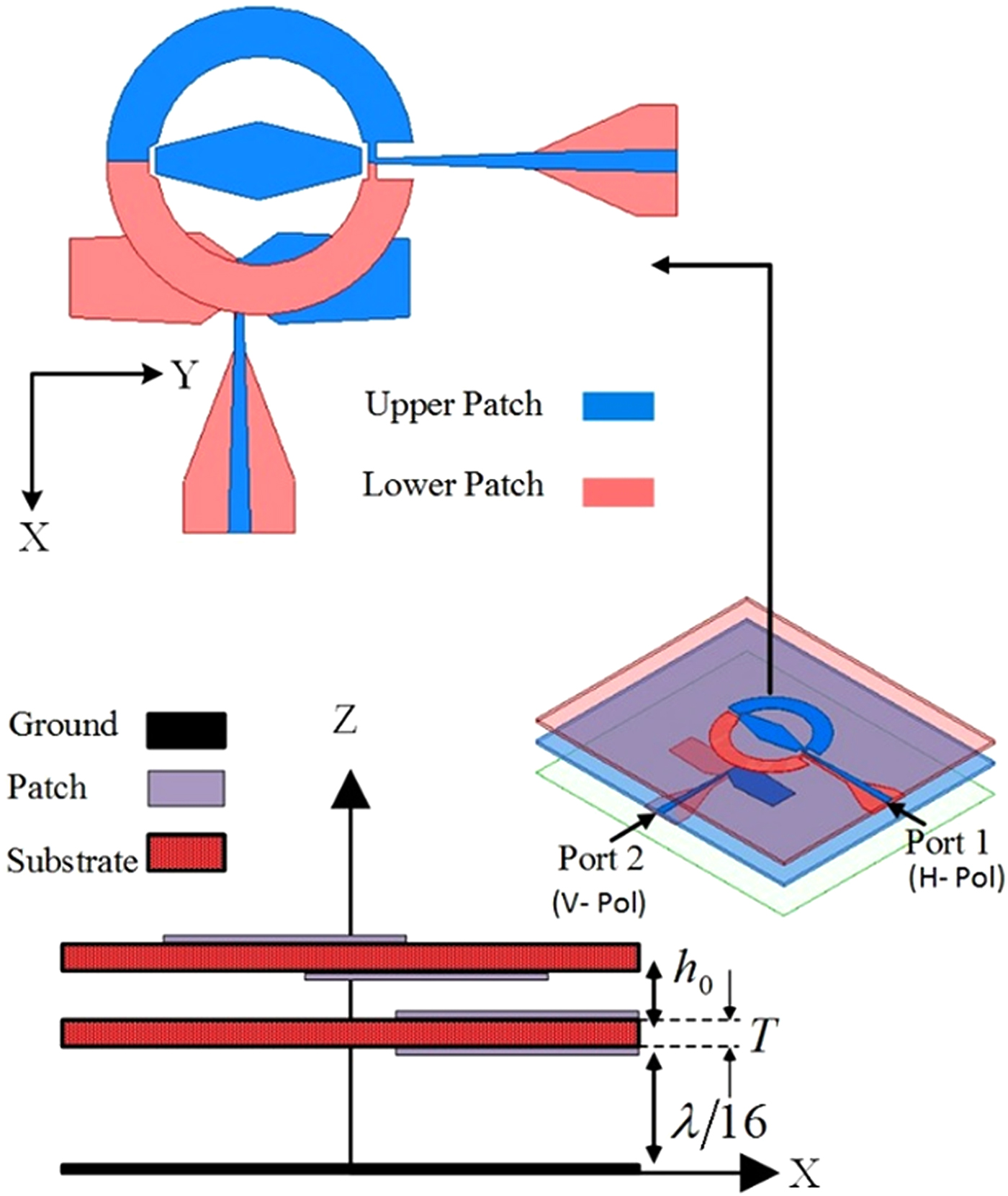
Fig. 1. Configuration of the proposed antenna. Upper and lower patches denote the patches that are placed at the top and bottom sides of the corresponding substrate.

Fig. 2. Demonstration of the geometry of (a) the printed dipole, (b) annular ring, and parasitic patch with their optimum design parameters as follows (in millimeter): WR1 = 6, WR2 = 7, WR3 = 3, LR1 = 10, LR2 = 4, L 1 = 6, L 2 = 18, L 3 = 4, W 1 = 8.5, W 2 = 1.8, W 3 = 0.8, W 4 = 0.7, R 1 = 8, R 2 = 11.8, Wb1 = 8.5, Wb2 = 1.2, Wb3 = 0.6, Wt1 = 1.7, Wt2 = 0.3, Lb1 = 3, Lb2 = 8, Lb3 = 12, Wc = 2.8, Lp = 15.7, Wp1 = 2, Wp2 = 6, T = 0.762 and h 0 = 5.5. The T parameter denotes the dielectric thickness.
The coupling between the radiation edges of the strip dipole as a driven element and four longitudinal edges of parasitic patch cause to enhance the impedance bandwidth. As will be shown later in the simulation results, surface current directions on the strip dipole and parasitic patch are similar. Notably, two another edges of the parasitic patch aligned near the radiating circular ring are small and make negligible effects on the impedance bandwidth of H-pol mode.
Optimum design parameters of two patches along with their balun and transition line specifications have been determined in Fig. 2. It is worthwhile to note that the well-known relation for the dipole length relative to resonant frequency can be used to get the preliminary assumption for the dipole length at the center frequency. Similarly, as the first assumption for parametric study of the antenna in the simulator, it may be valuable to use the relation between the mean circumference of the ring and its resonant frequency which is used in circular ring microstrip antennas [Reference Stutzman and Thiele17].
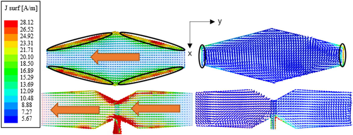
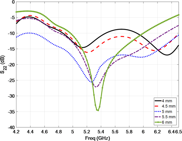
The full-wave simulation results based on the design parameters presented in Fig. 2 without using the parasitic patch (step 1) are depicted in Fig. 3, in which S 12 and S 11 quantities have acceptable amounts across the frequency band of interest. Figure 4 shows the result of the S-parameter after introducing the parasitic patch with optimum dimension to the structure. Clearly, S 22 quantity is greatly improved, meanwhile S 12 and S 11 parameters remained fixed approximately. The return loss are below −10 dB from 4.3 to 6.5 GHz (40% bandwidth) at port #1 and from 4.2 to 6.5 GHz (43% bandwidth) at port #2. Furthermore, the isolation between two ports is higher than 30 dB in a wide frequency band. Figure 5 shows the surface current density over the parasitic and corresponding radiating patches under two modes of excitation at 5.5 GHz. It was observed that the strip dipole makes a considerable effect on the parasitic patch when port #2 is excited. But, for the H-pol mode, when port #1 is excited, the coupling is negligible.

Fig. 3. S-parameter simulation results of antenna without parasitic patch.

Fig. 4. Simulation and measurement results of the S-parameters of antenna incorporating parasitic patch to the upper substrate.

Fig. 5. Demonstration of the surface current distribution of the parasitic patch and strip dipole when (a) port #2 is excited and (b) port #1 is excited. Major and minor edges of the parasitic patch has been highlighted.
It is worthwhile to note that the study of the full-wave simulation results shows that as the distance between two substrates is increased, the resonant frequency of the lower patch will be decreased. Hence, the dimensions of the lower patch can be decreased by increasing the h 0 parameter. Figure 6 depicts the effect of varying h 0 parameter on the return loss of port #2.

Fig. 6. Simulation results of the parameter S 22 as the distance between two substrates (h 0) is varied.
Experimental results and discussions
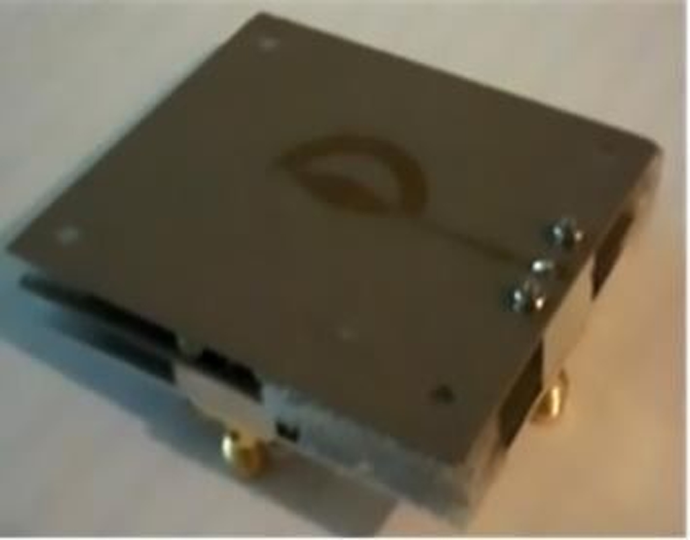
A prototype of the designed antenna was fabricated and the scattering parameters associated with two ports along with the far-field radiation patterns for both polarizations in two principal planes of the antenna (xoz- and yoz-planes) were measured. Figure 7 shows the manufactured antenna in which a foam spacer has been utilized to fix the air gap distance between two substrates and ground plane. The scattering parameters of the antenna (S 11, S 12, and S 22) were measured by the Agilent 8722ES Vector Network Analyzer. Figure 4 shows the simulated and measured S-parameters. As depicted in Fig. 4, the measured −10 dB impedance bandwidth is 40 and 43% for port #1 and port #2, respectively. The measured isolation between two input ports is below −35 dB within the frequency band from 5.2 to 5.8 GHz. As such, antenna enables to cover WLAN frequency band (from 5.2 to 5.8 GHz) properly with high polarization performance.

Fig. 7. Prototype of the proposed antenna.
Simulations and measurement results of co-polar and cross-polar radiation patterns of the antenna at YZ- and XZ-planes for both polarizations at 5.5 GHz are shown in Fig. 8. A quantitative study of the results show that the 3 dB beam widths of the patterns for both XZ and YZ-planes are 74.2 and 72.3° for port #1 and also 64 and 74.1° for port #2. The measured cross-polar levels at boresight in the XZ-/YZ-planes are below −16.3 and −25 dB at port #1 and −10.2 and −10.3 dB at port #2, respectively. The measured front-to-back ratio for both ports is more than 17 dB, which can be improved by increasing the dimensions of the ground plane. Moreover, measured gain versus frequency is shown in Fig. 9, which shows a gain of 8.7 dBi for port #1 and 8.5 dBi for port #2 at the design frequency of 5.5 GHz, respectively.

Fig. 8. Simulation and measurement radiation patterns in (a) XZ-plane for port #1, (b) XZ-plane for port #2, (c) YZ-plane for port #1, and (d) YZ-plane for port #2.

Fig. 9. Measured gain versus frequency for polarization corresponding to port #1 and port #2.
Conclusion
Design and implementation of a dual-polarized antenna consisting of a planar microstrip dipole and an annular ring has been described. The antenna was comprised of two separate dielectric layers and had a good port-to-port isolation. To achieve broad bandwidth from the strip dipole in the lower layer, a parasitic element on the upper substrate at the center of the annular ring element was used. The antenna exhibited measured −10 dB return loss bandwidth of 40% (4.2–6.5 GHz) and 43% (4.2–6.5 GHz) for port #1 and port #2, respectively. Moreover, the cross-polarization levels in both planes are better than −12 dB. The proposed dual-polarized antenna can easily be used in a large-scale arrays and also in applications requiring circular polarization. High gain, very good bandwidth, low cross-polarization level and good isolation between input ports make the antenna completely suitable for 5.2/5.8 GHz WLAN applications.
Acknowledgement
The authors would like to thank Iran Telecommunication Research Center (ITRC) for supporting this project.
 Majid Karimipour was born in Shahrekord, Iran, in 1986. He received the M.Sc. degree from the Shahid Beheshti University (SBU), Tehran, in 2011, in Electrical Engineering. He is currently working toward the Ph.D. degree in Communication Engineering in Iran University of Science and Technology (ISUT), Tehran, Iran. He is a member of the Applied Computational Electromagnetic Society reviewer group since 2013. His major research interests are the development and design of reflectarray and transmitarray antennas, phase array antenna, tracking radars, complex EM media, optimization algorithms, and numerical methods in EM.
 Iman Aryanian was born in Iran in 1986. He obtained his B.Sc. in Electrical Engineering from Amirkabir University of Technology, Tehran, Iran, in 2008. Then he received his M.Sc. in Electrical Communication Engineering from Amirkabir University of Technology, Tehran, Iran, in 2010, and his Ph.D. degree in the same field from Amirkabir University of Technology, Tehran, Iran, in 2016. Title of his M.Sc. thesis was “Design, simulation and implementation of a high efficiency wimax power amplifier using EER linearization technique” and title of his Ph.D. thesis was “Nonlinear analysis of reflectarray antenna and improving its performance in presence of active elements”. He is currently an Assistant Professor with the communication satellite group, Iran Telecommunication Research Center, Tehran, Iran, and his research area is about space antenna. He has authored or coauthored over 23 papers in refereed journals and local and international conferences. His research interests are in the areas of reflector and reflectarray antenna, computational electromagnetic, semiconductor RF modeling, electromagnetic theory, and computational electromagnetics.