I. INTRODUCTION
The ever increasing demand for energy harvesting has driven an explosive technology evolution in the advance of miniaturized electronic devices featuring light weight and portability. Among the energy harvesting applications, the inductive coupling technique featuring wireless power delivery and data communication has been emerged as one of the most powerful tool for reoperation-free energy supply and noninvasive vital sign monitoring of implantable sensor networks.
Thanks to the rapid advance in the technologies of integrated circuit (IC) during the last 10 years, it is possible to realize a complex signal processing system with large number of transistors in a single microchip, which creates the possibility of building chip-level implantable sensor networks. Such sensor networks of today may also be capable of reconstructing lost sophisticated human sensations. One of the successful examples is the cochlear implant. Combined with the cutting edge energy harvesting techniques, it has been able to be used to regain the great part of the sense of lost hearing.
Though such sensor networks have been extensively studied over the recent decade, there are, however, still many bottlenecks that need to be overcome. This paper aims for accomplishing a high-performance platform for such applications, especially those in want of being powered inductively. An efficiency-enhanced rectifier has been implemented for such applications. Moreover, it is with a miniaturized back telemetry technique for sending physiological data out of body. This builds up a simple data exchange approach from the inside to the outside. Our design can be easily applied to the other similar radio frequency identification (RFID)-based sensor network systems of medical uses, with only minor modification in the design itself.
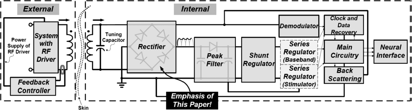
The role of the rectifier in a wireless energy harvesting system applied to biomedical sensor networks can be comprehended from the architecture shown in Fig. 1. The rectifier serves as the first stage for AC—DC conversion. In addition to the loss caused by the coils involved, it has been proved that significant portion of the degradation of the prosthetic system energy efficiency can be ascribed to the rectifier dropout voltage, as a result of the diode forward threshold voltage, when providing power supply to the integrated circuitry on the secondary side [Reference Ghovanloo and Najafi1, Reference Sauer, Stanacevic, Cauwenberghs and Thakor2].

Fig. 1. Representative architecture of a wirelessly powered energy harvesting system applied to implantable sensor networks.
Another important issue worthily noted is that the commonly used back telemetry mechanisms have not been optimized yet as far as the tradeoffs of its rectifier application among the system energy efficiency, dropout voltage caused by the additional switch for load-shift keying (LSK) modulation, and implementation area overhead is concerned [Reference Tang, Smith, Schild and Peckham3, Reference Wang, Liu, Sivaprakasam and Kendir4]. Furthermore, for back telemetry, providing the system with improved robustness against certain degrees of coils misalignments, motion artifacts, nearby metallic objects, and electromagnetic noise and interference is still an open requirement needing to be filled [Reference Atluri and Ghovanloo5].
The rest of the paper will elaborate on how the above mentioned issues are dealt with in circuit means and the measurement data obtained from the proof-of-concept prototypes.
II. PROPOSED DESIGN
AC–DC conversion performed with diode(s) causes at least one diode forward threshold voltage, which can be expressed as
 $$\left\vert {V_{TH}} \right \vert + \sqrt {\displaystyle{{2I_D} \over {\mu C_{ox} \left( {\displaystyle{W \over L}} \right)}}} \;,$$
where V TH is the metal-oxide-semiconductor (MOS) threshold voltage, μCox is the intrinsic transconductance, and W and L are the transistor width and length, respectively [Reference Ghovanloo and Najafi1], when a rectifier is implemented in complementary metal-oxide-semiconductor (CMOS) process. The diode forward threshold voltage considerably decreases the supply voltage VOUT to the implanted circuitry for a given transmitted power P TX and coupling factor. This means that for a required VOUT and given distance between the reader and transponder, P TX stemming from the current i TX driving the primary power amplifier must be considerably increased as VOUT is ideally a monotonic function of i TX [Reference Sauer, Stanacevic, Cauwenberghs and Thakor2]. The relationship between the device geometry ratios, specified system requirements for the current dissipated at the primary side i 1, output voltage of the rectifier VOUT, and other parameters can be expressed as [Reference Rendon-Nava, Díaz-Méndez, Nino-de-Rivera, Calleja-Arriaga, Gil-Carrasco and Díaz-Alonso6]
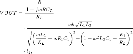 $$\eqalign{VOUT &= \displaystyle{{\displaystyle{R \over {1 + j\omega R{C_L}}}} \over {{R_L}}} \cr &\quad\cdot \displaystyle{{\omega k\sqrt {{L_1}{L_2}} } \over {\sqrt {{{\left( {\displaystyle{{\omega {L_2}} \over {{R_L}}} + \omega {R_1}{C_1}} \right)}^2} + } {{\left( {1 - {\omega ^2}{L_2}{C_1} + \displaystyle{{{R_1}} \over {{R_L}}}} \right)}^2}}}\cr &\quad\cdot {i_1},}$$
where L 1, L 2, R 1, C 1, and R L are the primary inductance, secondary inductance, secondary parasitic resistance, secondary resonant capacitance, and secondary load, respectively. A rectifier implemented in modern CMOS process can be expected to have considerably reduced substrate leakage current compared with its counterpart implemented in bipolar junction transistors (BJTs) [Reference Ghovanloo and Najafi1, Reference Sauer, Stanacevic, Cauwenberghs and Thakor2].
In response to the efficiency degradation caused by the diode(s), several state-of-the-art works have been demonstrated in the literature. In [Reference Ghovanloo and Najafi1], the authors employed cross-coupled power N-channel metal-oxide-semiconductor (NMOS) transistors in place of the diode-connected counterparts in the conventional full-wave rectifier to reduce the voltage drop for charging the capacitive load connected with VOUT. The authors of [Reference Sauer, Stanacevic, Cauwenberghs and Thakor2] presented another similar design where latch-up can be thoroughly prevented by taking advantage of all p-transistor implementation, without the employment of additional auxiliary transistors used to ceaselessly tie the bodies of the PMOS transistors to the highest voltage levels compared with that in [Reference Ghovanloo and Najafi1]. A comparatively different solution, using two active diodes achieving almost zero forward-voltage drop to replace the diode-connected power PMOS transistors in those proposed in [Reference Ghovanloo and Najafi1] and [Reference Sauer, Stanacevic, Cauwenberghs and Thakor2], has recently been presented [Reference Chen, Chen and Liu7].
Despite one diode existing in the conventional full-wave rectifier is eliminated for any of the three rectifiers, they still suffer from one diode threshold voltage drop in their conduction loops when functional. For implanted medical transponders based on RFID technology to provide the researchers with internal information (telemetry for sending data outside body) – neural recording for example, the recorded neural signal after filtering and amplifying is digitally quantified prior to being transmitted for the most part, in order to achieve robust communication. The binary data representing the neural signal can be load-modulated on the secondary side and demodulated on the external primary side, known as the LSK back telemetry.
In general, when R, modeling the average resistance equivalent to the implanted active circuitry, is large, a parallel MOS switch to short the coil inductor on the secondary side ahead of the rectifier for a short period of time can be used for LSK [Reference Atluri and Ghovanloo5]. On the other hand, a series MOS switch can be used after the rectifier to open the loads when R is small, causing additional dropout voltage and consequently degrading the system energy efficiency when the switch is on [Reference Wang, Liu, Sivaprakasam and Kendir4].
As a matter of fact, either of the two conditions demands to minimize the resistance to the MOS switch in order for sufficiently small dropout voltage and sufficiently large impedance change of LSK, resulting in the penalty of huge area overhead. The design proposed in this paper incorporated an efficient back telemetry mechanism with the rectifier to not only thoroughly address the diode concern but also deal with the problems in the commonly used LSK technique, which will be detailed in the following paragraph.
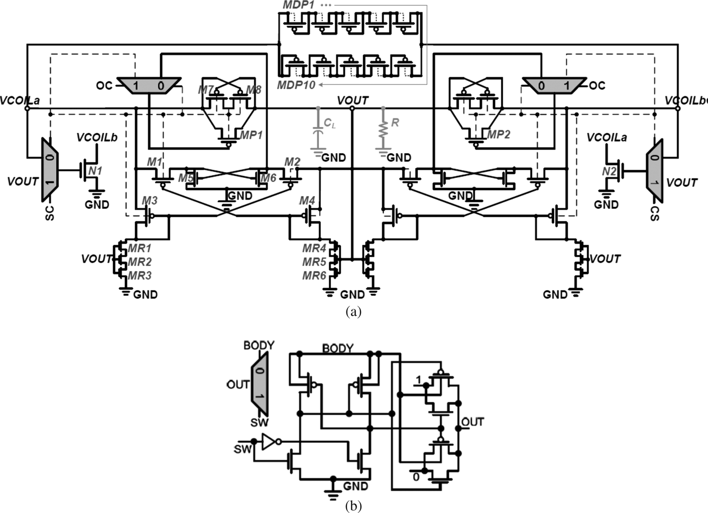
Shown in Fig. 2(a) is the circuit schematic of the rectifier. It has two symmetrical parts the same as those shown in [Reference Chen, Chen and Liu7], with the exception of the connections of the power transistors, N1 and N2, and four 2:1 multiplexers. These multiplexers make it a rectifier with three operating modes Rectification (SC, OC = 0, 0), Open Coil (SC, OC = 0, 1), and Short Coil (SC, OC = 1, 0) [Reference Atluri and Ghovanloo5]. By symmetry, steady-state operation of the rectifier can be explained using only the left half part.
Fig. 2. Proposed low-loss rectifier with built-in back telemetry mechanism. (a) Rectifier main body. (b) Schematic diagram of multiplexer.
When operated in Rectification, each multiplexer chooses its input “0” as the gate driving potential of the corresponding power MOS. During the first half part of each AC voltage source period (i.e. VCOILa rises from its wave trough to peak), N1 first turns on and creates a conduction path from the referred ground GND to VCOILb. According to the explanation of [Reference Chen, Chen and Liu7], the drain voltage of M4, namely the gate voltage of M1, will be VOUT − |Vt M4|. MP1 then turns on when VCOILa > VOUT − |Vt M4| + |Vt M1|. It means that the drop-out voltage can be minimized if |Vt M4| is close to |Vt M1|.
On the other hand, during the second half part of each AC voltage source period, MP1 first becomes off as long as VOUT > VCOILa − |Vt M3| + |Vt M2|. When VCOILa − VCOILb < V t N1, N1 then turns off and cuts the conduction loop short. M7 and M8 function as the auxiliary transistors seen before. In order for optimal AC–DC conversion efficiency, MR1–MR6 should be designed in small-width and long-length transistors.
Operation of the right half part is identical to that of the left half part except that VCOILa and VCOILb are interchanged in analysis. It is obvious that, for the proposed design, there exists no diode voltage drop in the course of charging C L; thereupon the loss in AC–DC conversion is minimized compared with that presented in [Reference Chen, Chen and Liu7]. C L and R, brushed and connected with gray lines, are the loads not on-chip. The modified circuit configuration of N1 and N2 is the key to the efficiency enhancement. The threshold voltage drop cancellation feature of the rectifier is competitive with those demonstrated in the literature. An innovative cancellation circuit has been proposed to compensate the voltage drop by applying an external bias [Reference Umeda, Yoshida, Sekine, Fujita, Suzuki and Otaka8]. The applied bias is between the gate and source terminal of the diodes. However, the circuit is not on-chip design. Further improvement on the cancellation circuit in [Reference Umeda, Yoshida, Sekine, Fujita, Suzuki and Otaka8] was investigated and achieved in [Reference Nakamoto9]. Despite its fully on-chip implementation, ferroelectric capacitor is needed and special process masks are unavoidable, resulting in potentially higher manufacturing cost. Our work can be designed completely in standard CMOS technology without special process masks.
When operated in Open Coil, the gates of MP1 and MP2 are driven by their body potentials, detaching the loads from receiver LC tank. This makes the coil on the secondary side faces high impedance, and ideally reduces the reflected impedance onto the external reader to its maximum value estimated by [Reference Atluri and Ghovanloo5]
 $$\displaystyle{{\omega ^2 k^2 L_1 L_2 \; \; \;} \over {R_2}}\!,$$
where k, L 1, L2, and R 2 are the coupling factor, primary coil inductance, secondary coil inductance, and parasitic resistance of the secondary coil, respectively. As for the Short Coil mode, MP1 and MP2 behave as if they are in the Rectification mode except that N1 and N2 are kept on continuously (their gates follow the VOUT terminal), resulting in the reflected impedance onto the external reader ideally reaches its minimum value estimated by
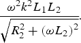 $$\displaystyle{{\omega ^2 k^2 L_1 L_2 \; \; \;} \over {\sqrt {R_2 ^2 + \left( {\omega L_2} \right)^2}}}\!.$$
In additional to the several details regarding rectifier operation, the used 2:1 multiplexers shown in Fig. 2(b), which converts the low-swing SW signal to the high-swing counterparts to fully pass the selected source signal to OUT, as well as the feedback keeper loop formed by MDP1–MDP10, which starts shunting current from one coil terminal to the other while the span voltage across the coil is higher than about 3.4 V [Reference Li and Liu10], should also be highlighted. The HSPICE simulation results of the 2:1 multiplexers demonstrating the functionality are shown in Fig. 3. It can be easily understood that the proposed rectifier, with the integrated multiplexers achieving built-in back telemetry inside, not only eliminates the additional switch size requirements for the conventional counterpart in either of minimizing the open-coil-used switch turn-on span voltage and maximizing the short-coil impedance change, but also theoretically reaches the maximally changeable impedance values in LSK.
Fig. 3. Post-layout simulation results of 2:1 multiplexers.
III. EXPERIMENTAL SETUP AND RESULTS
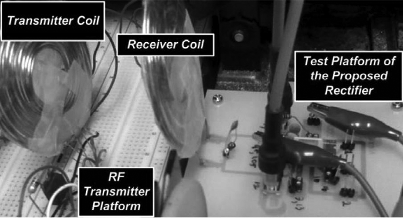
We have implemented the proposed rectifier whose micrograph is shown in Fig. 4 in a 0.18 μm 1P6M standard CMOS process. The design occupies 0.049 mm2. To measure the system, we have built a platform, shown in Fig. 5, using international rectifier corporation (IRF) power devices with resonant network at primary side. We have made hand-wound spiral coils with 16 turns at both sides for testing purpose. The pancake-shaped coils were made from copper wires and the transceiver was tuned to be operated at 2 MHz in carrier frequency for all the passive components involved. The primary and secondary sides were moved apart. The two coils were center-aligned. To give better insight into how good the performance of the system can be achieved, both coupling efficiency of the coils at various distances and their dropout percentage at various thicknesses of Ringer's solution in the middle between the two coils to emulate truly human biology nature have been carried out. The results shown in Fig. 6 can be used to provide a decent idea of the performance on the built platform.
Fig. 4. Chip photomicrograph.
Fig. 5. Measurement setup.
Fig. 6. Coupling efficiency (in air) versus percentage drop (with the Ringer's solution in between). The symbols of “*” and “Δ” indicate “Percentage drop versus thickness” and “RMS coil voltage versus coil distance”, respectively.
In addition to the experimental results obtained from the transceiver coils and their connected resonant networks at the primary and secondary sides, the performance of the proposed CMOS rectifier with back telemetry should be characterized specifically to be given as proof of concept. The experimental conversion efficiency of the proposed rectifier versus R under a carrier frequency of 2 MHz, C L = 0.1 μF, and |VCOILa − VCOILb|peak = 3.3 V is shown in Fig. 7. For a fixed R of 1 kΩ, plots of the conversion efficiency data on several carrier frequencies are revealed in Fig. 8. The chosen carrier frequencies have been clinically demonstrated that they are acceptable and applicable to the medical implants [Reference Wang, Liu, Sivaprakasam and Kendir4, Reference Rendon-Nava, Díaz-Méndez, Nino-de-Rivera, Calleja-Arriaga, Gil-Carrasco and Díaz-Alonso6].
Fig. 7. Conversion efficiency versus resistive load. VCE means voltage conversion efficiency.
Fig. 8. Conversion efficiency with respect to carrier frequency.
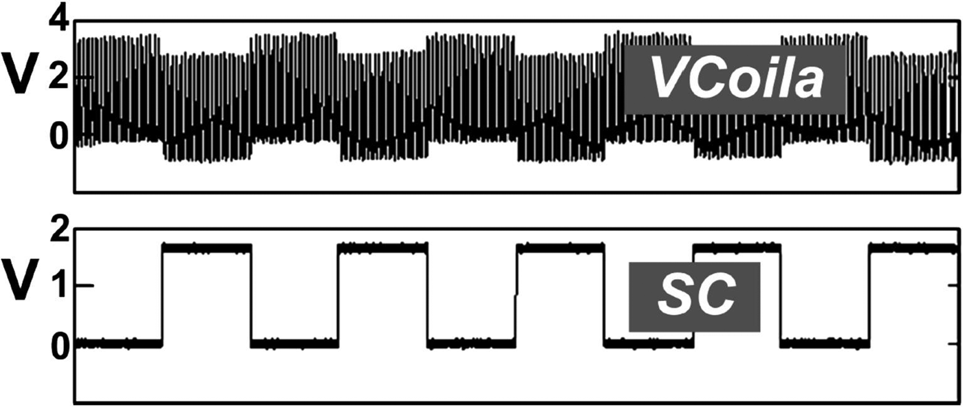
With regards to the results, power conversion efficiency (PCE) of the proposed rectifier degrades significantly for smaller R, which can be attributed to acutely increased requirement for the power input to rectifier. PCE also degrades with increased R as the gradually decreased power transferred to the loads dominates. In addition, implemented has the conversion efficiency degrading with increased carrier frequency, mostly as a result of the monotonicity between the drop-out voltage of VOUT and carrier frequency. Figure 9 shows the oscilloscope trace of the fabricated rectifier IC demonstrating the short-coil LSK functionality. Similar waveforms have also been observed in the prototypical chip for open-coil functionality. In summary, proposed is competitive with those demonstrated in the literature, which can be established in Table 1.
Fig. 9. Oscilloscope trace of the rectifier operating at short-coil mode.
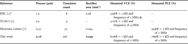
Table 1. Comparison table of measured rectifier results.
VCE, voltage conversion efficiency; PCE, power conversion efficiency
– Not available in terms of rectifier.
* Standard CMOS version of the design proposed in [Reference Ghovanloo and Najafi1].
![]() According to Fig. 9(a) in [Reference Ghovanloo and Najafi1].
According to Fig. 9(a) in [Reference Ghovanloo and Najafi1].
† With multiplexers achieving built-in back telemetry mechanism.
Despite the rectifier-only conversion efficiency of 90% recorded, more detail needs to be given to explain the end-to-end “DC-load efficiency”. Definition of the DC-load efficiency can be found in [Reference Pinuela, Yates, Lucyszyn and Mitcheson11]. The DC-load efficiency includes the driver efficiency at the transmitter, the coil coupling efficiency, the rectifier efficiency, and the regulator efficiency. The regulator, the circuit beneath the rectifier, can have many types of circuit structure and is not the focus of this paper. Its efficiency may vary significantly, depending on design and application. From our experimental setup, the class-E driver efficiency is about 67%, due to semiconductor losses. The average coil coupling efficiency at a distance of 0–6 cm is about 3% for our hand-made coils. Assuming that the regulator efficiency can be as high as 90% for a DC-DC converter, these can be used to obtain a DC-load efficiency of about 1.6%.
VI. CONCLUSION
A high-efficiency and cost-effective rectifier integrated with a full-custom wireless powering platform has been presented for biomedical sensor network applications. With the novel energy harvesting circuit techniques of negative-resistance configuration in power NMOSs and multiplexer-based LSK, the design fulfills the following achievements: (1) almost zero forward voltage drop in rectification (2) back telemetry mechanism with significantly more robust and lower area overhead than the most commonly used counterpart. Experimental results from the fabricated chips demonstrate that the entire system is fully functional and capable of providing both power delivery and data communication with low cost and high efficiency. The new-generation almost ideal-switching rectifier with built-in back telemetry mechanism provides a powerful and promising tool for the chronic transcutaneous applications requiring reoperation-free noninvasive powering.
ACKNOWLEDGEMENTS
This study was supported in part by the Ministry of Science and Technology, Taiwan, under grant Nos. 103-2221-E-182-070 and 102-2218-E-182-003. The author would also like to thank funding support from the Chang Gung University and Chang Gung Memorial Hospital under grant Nos. UERPD2D0051 and CMRPD3D0221.
Statement of interest
The authors declare that there is no conflict of interests in this paper with any trademark or software mentioned.
Cihun-Siyong Alex Gong has been involved in biomedical circuits and systems since starting his M.S. program. He received the B.S. degree in Civil Engineering, the M.S. degree in Biomedical Engineering, and the Ph.D. degree in Electrical Engineering, in 2002, 2005, and 2008, respectively. In 2009, he joined the Industrial Technology Research Institute, Hsinchu, Taiwan, as one of the Research and Development Staff Members. He held Adjunct Assistant Professor position at National Taiwan Normal University, Taipei, Taiwan, and National United University, Miaoli, Taiwan, in 2012 and 2013, respectively. He joined the Department of Electrical Engineering, School of Electrical and Computer Engineering, College of Engineering, Chang Gung University, Taoyuan, Taiwan, in 2013, where he is currently an Assistant Professor and with the Portable Energy System Group, Green Technology Research Center. His research interests are in electronics for medicine and healthcare, including interfacing-associated solid-state circuits and their physiological issues. He chaired the sessions on Advanced Circuit and System on Green and Biomedical Applications, Information and Communication Technology for Translational Medicine and Green Applications, and RF and Wireless for the IEEE ISCE 2013, the IEEE ICCE-TW 2014, the IEEE ICCE-TW 2015, and the IEEE ICCE 2015, respectively. Dr., Gong has been Technical Program Committee member of the conferences and was a recipient of the 2004 Domestic Annual Symposium on Biomedical Engineering Excellent Paper Awards, the 2005 NYMU Honours Student Awards in memory of the Yin, Syun-Ruo, the 2008 NCU Outstanding Graduate Student Awards, the Best Student Paper Contest Awards in the 2008 IEEE International Conference on Electron Devices and Solid-State Circuits, the 2009 Best Design Awards of the CIC, Taiwan, the 2009 Taipei International Invention Show and Technomart Gold Medal Awards, the 2012 Best Paper Awards of the CCL Technical Journal, the Honorable Mention Awards at the 2013 Biomedical Engineering Symposium on 4B, Taiwan, and the Honorable Mention Awards at the IEEE ICCE-TW 2014. Prof. Gong founded MIX studio, Taiwan, and was working for Merry Monarc(h) studio, Taiwan, prior to his academic career.