I. INTRODUCTION
Microstrip patch antennas have been one of the favored choices in research and industry for use in radio frequency (RF) handheld devices. The main reason for this can be attributed to the continuous shrinking size of electronic equipment that demands same type of antenna elements in wireless devices. Apart from the issue of size compatibility, the radiation properties of the antenna should also be sufficiently suitable for the desired applications. A microstrip antenna (MSA) fulfills all these requirements needed to support RF handheld devices for a specific wireless application. Apart from having a compact geometry, these antennas are low cost, easy to manufacture and conformable to planar as well as non-planar surfaces [Reference Balanis1]. Apparently, a major challenge among researchers has been to get a broadband behavior from these antennas as these antennas suffer from an inherent disadvantage of low bandwidth (up to 5% around the center frequency of operation). Literature review in the context of bandwidth enhancement of MSA reveals a number of methods for improving the impedance bandwidth (voltage standing wave ratio – VSWR < 2) of these antennas. The proposed methods mainly include the use of slot-loaded patch antennas for a wideband antenna performance [Reference Weigand, Huff, Pan and Bernhard2], use of spiral-shaped antennas to get a dual wideband performance [Reference Kaur3], use of typical shapes like “E”-shaped patches to improve operational bandwidth of MSA [Reference Chen, Yang and Nie4] and planar inverted F antenna (PIFA) structures to enhance the bandwidth [Reference Virga and Rahmat-Samii5]. Many other techniques that are available for bandwidth enhancement are mentioned in [Reference Manassas, Kaifas and Siakavara6–Reference Best8]. Stacking of multiple patch antennas printed on different substrate layers was introduced by Waterhouse [Reference Targonski, Waterhouse and Pozar9]. Stacking antenna layers has been a preferred choice to achieve a multiband and wideband performance among researchers, because of its ease of implementation. Research work is available in [Reference Kaur, Khanna and Kartikeyan10, Reference Kaur, Khanna and Kartikeyan11] that concentrate on the development of stacked patch antennas for multiband and wideband wireless applications. Defected Ground Structures also aid in obtaining a multiband and a wideband operation from the microstrip patch antennas [Reference Sharma, Chakravarty and Bhooshan13, Reference Yadav and Vishwakarma14].
Based on the literature review in this regard [Reference Palandoken and Nasimuddin16], a novel technique has been proposed in this paper for bandwidth enhancement. The main aim of this novel technique is to utilize slot loading a patch antenna in a stacked configuration with a defected ground structure for enhancing the bandwidth of conventional microstrip patch antenna. The slot is introduced in the parasitic patch such that the driven patch is approximately of same dimensions as the slot in parasitic patch, thereby forming a complementary geometry stacked antenna that shows an ultra-wideband (UWB) behavior. Another aim is to use a feed line that has a horizontal stub attached to it for exciting the patch and thereby allows the antenna to exhibit a circularly polarized behavior.
As the UWB, wireless local area networks (WLAN), Unlicensed National Information Infrastructure band (UNII), Worldwide Interoperability for Microwave Access (WiMAX), and Radio Astronomy are some of the most prominent wireless technologies used these days for wireless data transfer; the aim of the proposed research work is to present an UWB antenna that supports a good data rate for the mentioned wireless applications of interest. Therefore the current article presents the design, development and experimental testing of a three-layered stacked aperture-coupled microstrip patch antenna with a complementary geometry. The antenna layers are stacked without any air gap between the substrate layers and the use of two stacked complementary-shaped patches that excite nearby frequencies leads to an increased operational bandwidth. The bandwidth is also improved by multiple-layered structures as it leads to an increased effective antenna height, thereby providing loosely bound fields that are radiated by the antenna [Reference Kaur, Khanna and Kartikeyan10]. The ground layer has a “π”-shaped slot cut from its surface apart from the aperture slot that further enhances the operational bandwidth of the antenna [Reference Arya, Kartikeyan and Patnaik12]. This stacked antenna is energized using a feed line that has a horizontal stub attached to it giving it a “T”-shaped geometry, this enables it to radiate two orthogonal linear (horizontal and vertical) components of electric field vector thereby emitting circularly polarized electromagnetic (EM) waves in free space.
The proposed antenna is designed and simulated using CST MWSV'10 software using Time domain solver and assuming the boundary approximations to be perfect. Antenna testing is experimentally performed using a VNA and an anechoic chamber for the authentication of results. A close match between the simulated and measured results allows the intended antenna to be an optimum choice for the suggested wireless applications of interest.
II. ANTENNA GEOMETRY
The perspective view of the proposed stacked resonant structure can be seen in Fig. 1(a). The aim of the antenna design is to get a circularly polarized UWB behavior from a stacked complementary MSA configuration that is fed with a T-shaped feed line. Therefore the antenna design procedure starts with the use of transmission line equations mentioned in C.A. Balanis for calculating the dimensions of the two rectangular patches (used in the stacked geometry) that excite two nearby resonant frequencies of 5.25 and 5.65 GHz [Reference Balanis1]. Since two patches are stacked, the two bands radiated by the antenna merge to show a broadband behavior.

Fig. 1. (a) Perspective view of the stacked antenna with three layers of dielectric substrate. (b) Topmost layer of the antenna. (c) Middle layer of the antenna. (d) Ground layer with π-shaped slot. (e) Bottom layer of antenna with a T-shaped feed line.
A slot is cut in the parasitic patch of approximately the same dimensions as the driven patch, allows one more current loop to be generated on the top patch and leads to an increase in the antenna operational bandwidth. Since the effective height for the parasitic patch increases, this slot excites an additional frequency near the resonance of 5.65 GHz that is governed by the equation (1) and further leads to enhancement of the antenna impedance bandwidth.
 $$f_r = \displaystyle{c \over {2(l_2 + \Delta l_2 )\surd \varepsilon _{2e}}}, $$
where ε2e
= (ε
r2 + 1)/2 + (ε
r2 − 1)/2(1 + 12(h
2/w
2))−1/2 and
 $\Delta l_2 = 0.412l_2 \displaystyle{{(\varepsilon _{2e} + 0.3)((w_2 /h_2 ) + 0.264)} \over {(\varepsilon _{2e} - 0.258)((w_2 /h_2 ) + 0.8)}}. $
And l
2 is the length of the slot cut in parasitic patch [Reference Yadav and Vishwakarma14].
$\Delta l_2 = 0.412l_2 \displaystyle{{(\varepsilon _{2e} + 0.3)((w_2 /h_2 ) + 0.264)} \over {(\varepsilon _{2e} - 0.258)((w_2 /h_2 ) + 0.8)}}. $
And l
2 is the length of the slot cut in parasitic patch [Reference Yadav and Vishwakarma14].
The proposed antenna is made up of three layers of the commercially available glass-reinforced epoxy laminate FR4 substrate. This substrate has a dielectric constant ε r of 4.4 with a dielectric loss tangent of 0.0024 and a thickness of 1.57 mm. The dimensions of substrate for all the three layers of the antenna are 47 × 35 mm2. The topmost two layers of FR4 have rectangular patches printed over them that have a complementary geometry with optimized dimensions of 27 × 27.25 mm2 (see Fig. 1(b)) and 13.8 × 10.125 mm2 (see Fig. 1(c)), respectively. The lower patch antenna is approximately of the same size as the slot dimensions in the upper patch antenna, which is 14 × 9.5 mm2; thus making it suitably called as a complementary stacked patch antenna.
The ground plane has optimized dimensions X4 × W4 as 44 × 38.5 mm2 (reduced ground) and a “π”-shaped slot is etched from its surface apart from the aperture slot that further enhances the bandwidth at the operational band (see Fig. 1(d)). A defected ground structure (DGS) behaves like an LC circuit that can excite another resonant frequency that is governed by the equation
 $$f_{r} = \displaystyle{1 \over {2\pi \sqrt {LC}}}, $$
where
 $L = 1/(4\pi ^2 f_o ^2 C)$
and
$L = 1/(4\pi ^2 f_o ^2 C)$
and
 $$C = \displaystyle{{f_c} \over {2Z_o}}. \displaystyle{1 \over {2\pi \,(\,f_o ^2 - f_c ^2 )}},$$
where f 0, f c , and Z 0 denote the resonant frequency, cut-off frequency, and characteristic impedance of microstrip line above the DGS, respectively
If the resonant frequency generated by the DGS is chosen close to the existing resonant frequency near 5.65 GHz, it further leads to an increase in the operational bandwidth of the antenna [Reference Arya, Kartikeyan and Patnaik12].
The antenna parameters for desired results are optimized by iterative procedure using the CST MWS V'10 software. The main parameters that were optimized to obtain the desired UWB behavior from the antenna are the driven patch length, aperture slot width and the width of the horizontal slot in DGS. Parametric variations mentioned in Section III elaborate the optimization procedure in detail.
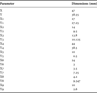
The antenna is excited by pulsed source using a feed line with a stub that forms a “T”-shaped geometry. This allows two orthogonal linear components of electric fields to be available on the antenna surface. Thereby allowing the antenna to radiate circularly polarized waves (see Fig. 1(e)). The parametric values of all the labeled parts of the antenna are mentioned in Table 1 for reference.
Table 1. Parametric details of the antenna.

III. SIMULATION RESULTS AND PARAMETRIC VARIATIONS
The proposed stacked antenna structure was designed and simulated in CST MWS V'10 using the Finite Integration technique and considering perfect boundary conditions. Simulation settings of hexahedral mesh cells with 30 lines per λ were chosen. The impedance-matching conditions required the antenna to be matched to a port impedance of 50 Ω and the results were analyzed using transient solver. Simulation results in terms of impedance bandwidth, axial ratio bandwidth, Smith chart, current distribution, and radiation pattern plots in terms of gain are presented in this section, for the antenna operating in the Quasi-TEM mode. The parametric variations and the effect of DGS are also mentioned to obtain the desired performance in terms of impedance bandwidth.
A) Impedance bandwidth
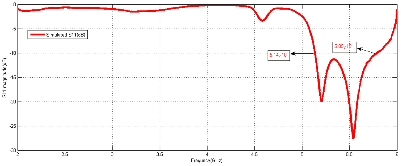
The frequencies for which the proposed antenna shows a S 11 (dB) value of −10 dB and below represent the impedance bandwidth for this antenna. Figure 2 shows the impedance bandwidth of 710 MHz for the proposed antenna from 5.14 to 5.85 GHz. Thereby showing a fractional bandwidth of 12.62% at the central frequency of 5.5 GHz (at the band of antenna's operation). This range of frequencies for which the proposed antenna's input impedance is matched to the impedance of the transmission line and the SMA connector (with an impedance of 50 Ω) is the required impedance bandwidth of the antenna.

Fig. 2. Simulated S 11 (dB) plot of the antenna.
Figure 2 shows the graph of the impedance bandwidth, with frequencies plotted along the X-axis against the S 11 (dB) values on the Y-axis.
B) Smith chart
The proposed stacked patch antenna is designed and simulated with a drive point impedance of 50 Ω. Figure 3 shows the Smith chart of the proposed stacked patch antenna and markers show the impedance matching at the band of antenna's operation.
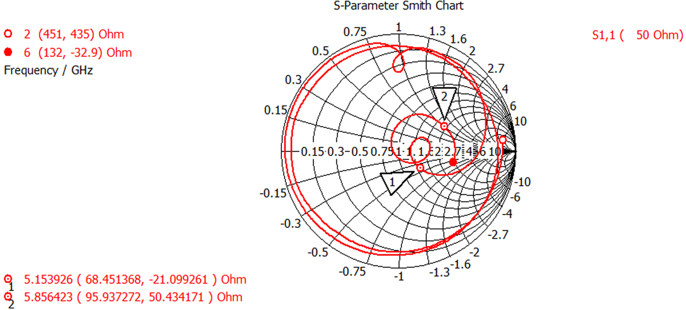
Fig. 3. Simulated Smith chart plot of the antenna.
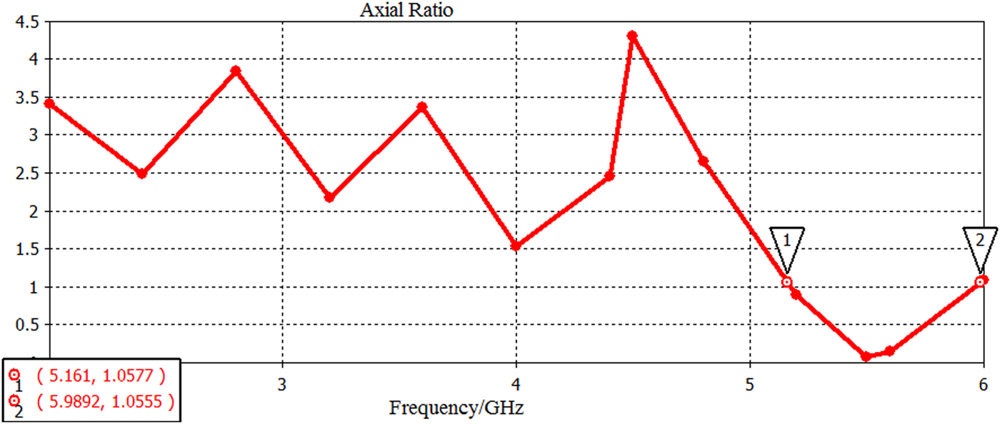
C) Axial ratio bandwidth
The range of frequencies at which the proposed antenna maintains the major to minor axis ratio of the ellipse (that is traced by the extremity of the two orthogonal electric filed components radiated by the antenna) is its axial ratio bandwidth. The 1 dB axial ratio bandwidth of the antenna is 819 MHz ranging from 5.16 to 5.98 GHz (see Fig. 4). The antenna radiates circularly polarized EM waves as two orthogonal linear components of electric field are emitted out by it in free space. Thus, the antenna shows a circularly polarized behavior at the operational band, thereby making it best for RF front end applications where the orientation of receiver will not affect the system's performance because of its ability to transmit and receive EM signals along any direction.

Fig. 4. Simulated axial ratio bandwidth of the antenna.
D) Current distribution results
In order to observe the responsibility of a specific part of the antenna for showing resonance at the respective frequencies of the operational band from 5.14 to 5.85 GHz, the antenna is energized with an input of 1 W (default) of power by the CST MWSV.10 software. The resulting distribution of current density is observed on different antenna layers for each respective resonant frequency. Figures 5(a) and 5(b) show the distribution of current on the surface of top and the middle patch antennas at 5.25 GHz. Since upper patch is shows a smaller value of current density (23.3 A/m) than that of 30 A/m on the lower patch antenna, the driven/lower patch is therefore considered to be responsible for the exhibiting the resonant frequency of 5.25 GHz. Figures 6(a) and 6(b) also show the peak values of surface current at the central frequency of the band at 5.5 GHz . The peak magnitude of surface current density on the top patch is 19.5 A/m and that on the lower patch antenna it is 17.15 A/m showing almost the same value of current at the center frequency of operation band, that leads to the conclusion that both the patches excite nearby frequencies of 5.5 GHz that merge to show a broadband operation. Figures 7(a) and 7(b) show the surface current distribution on the two patches at 5.65 GHZ. The simulation results show that the upper patch antenna has a peak surface current distribution of 20.38 and 15.48 A/m on the lower patch. This further leads to the conclusion that the upper patch that has two current loops formed at its surface is responsible for exhibiting a resonant frequency of 5.65 GHz. Figure 8 shows the current distribution on the ground plane at 5.5 GHz is 29 A/m. Therefore the ground structure further helps in enhancing the antenna bandwidth and this is elaborated in Section III-E of the paper.

Fig. 5. (a, b) Surface current distribution on the upper and lower patch antennas at 5.25 GHz.

Fig. 6. (a, b) Surface current/H-field distribution on the upper and lower patch antennas at 5.5 GHz.

Fig. 7. (a, b) Surface current distribution on the upper and lower patch antennas at 5.65 GHz.

Fig. 8. Current distribution on the ground plane at 5.5 GHz.
E) Role of DGS in bandwidth enhancement
A DGS is usually a slot of a specific shape cut out in the ground layer of the antenna. This slot in the ground layer disturbs the current distribution there and changes the frequency-dependent inherent inductive effect of the resulting structure. This changes the propagation of EM waves through antenna substrate layers and thus a specific resonance can be obtained from these structures too. If the resonance is close to the operational band of the antenna, it can lead to an improved bandwidth. In case it produces a new resonance, the antenna structure behaves as a multiband antenna [Reference Arya, Kartikeyan and Patnaik12]. The S 11 (dB) plot of the antenna (with respect to frequency) that compares the antenna operation with and without DGS is shown in Figure 9. It can be observed from Fig. 9 that the proposed antenna structure with DGS shows an increase in bandwidth by 200 MHz as compared with the antenna without DGS. The DGS thus helps in improving the antenna performance.
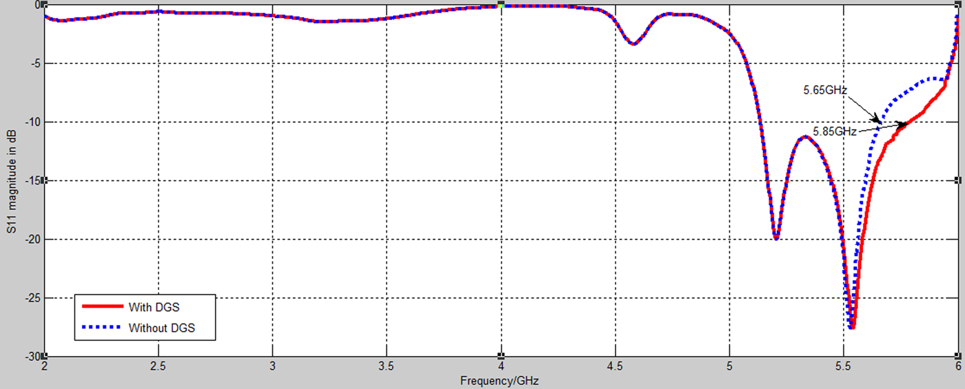
Fig. 9. Comparison of S 11 (dB) value of the antenna with and without a DGS.
F) Parametric analysis of the antenna
The antenna parameters for the required impedance bandwidth of 710 MHz from 5.14 to 5.85 GHz have been optimized using the parameter sweep option in the software CST MWSV'10. Figure 10 shows the parametric results of antenna in terms of the S 11 (dB) plot. These results were obtained when the length of patch was varied, it is observed from Fig. 10 that with variation in the upper patch length, the S 11 (dB) values vary and since lower values of S 11 (dB) are preferred for antennas with a better impedance matching, 27 mm (−13.5 to 13.5 mm) was chosen as the optimized length of upper patch antenna.
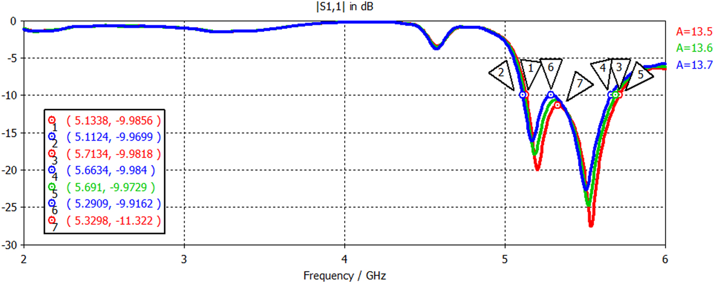
Fig. 10. Effect of variation in the length of upper (parasitic) patch antenna.
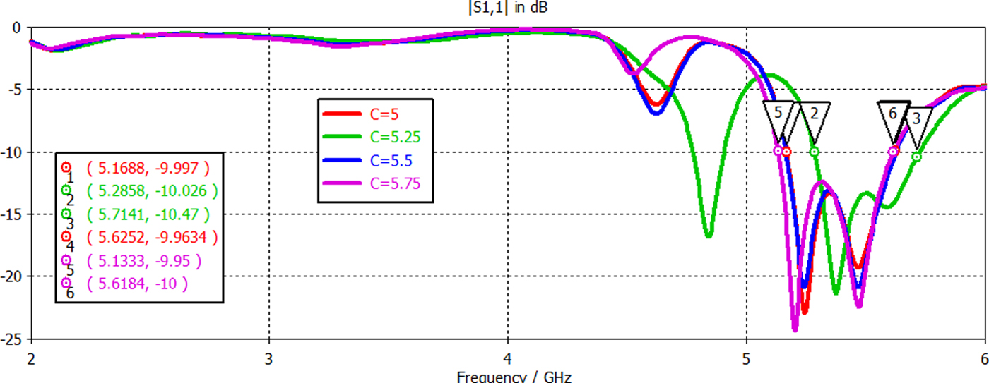
Another parameter that was optimized was the DGS parameter X7. From Figure 11, it is observed that the value of S 11 (dB) as well as impedance bandwidth gets affected when the DGS dimensions are changed. The optimized value of X7 is therefore chosen to be 7.5 mm for the proposed patch antenna.
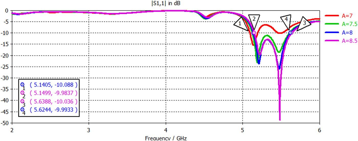
Fig. 11. Effect of variation in the length (X7) of DGS.
Figure 12 shows the variations on the shows the effect of variation of aperture slot width Y7 on the S 11 (dB) results of the antenna, the variation in the height of the aperture slot leads to shift in the resonant frequency as the major portion of the energy gets coupled to the patch through this slot only. Since the best results are obtained with a slot width equal to 0.5 mm, i.e. from 5.25 to 5.75 mm, the optimized height of the slot is selected to be 0.5 mm.

Fig. 12. Effect of variations of aperture slot Y7 on antenna performance.
IV. ANTENNA FABRICATION AND MEASUREMENT RESULTS
The proposed optimized stacked patch antenna was fabricated using chemical lithography technique on an Fr4 substrate that has a thickness of 1.57 mm and a loss tangent of 0.0024. Figure 13(a) shows the view of stacked patch antenna structure with three layers and Fig. 13(b) shows the view of defected ground plane of antenna with a slot (“π” shape) etched out from its surface. The ground layer has an aperture slot at the center apart from the “π”-shaped slot. The antenna was experimentally tested using a Vector Network Analyzer E5071C that has an operating range of 9 KHz to 8.5 GHz for impedance bandwidth measurements. Measurements were also made in a reflection-free chamber that operates at a frequency range between 2 KHz and 20 GHz. This chamber had a standard horn antenna with a calibrated gain of 12 dBi for Gain measurements.

Fig. 13. (a) Front view of the assembled antenna (b): View of the ground plane of antenna with a pie shaped slot.
Figure 14 shows the correlation between simulated and measured results, which are plotted using MATLAB 2007b.
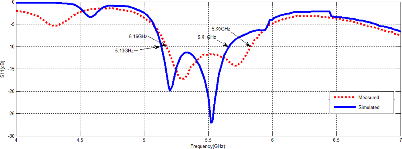
Fig. 14. Correlation between simulated and measured impedance bandwidth results.
Figure 14 reveals that simulated impedance bandwidth is from 5.13 to 5.85 MHz and the measured impedance bandwidth is from 5.16 to 5.9 GHz, which allows the antenna to be efficiently used for UWB bands from 5.28 to 5.85 GHz, IEEE802.11a/WLAN applications from 5.15 to 5.35 GHz, a IEEE 802.11b/WLAN band from 5.75 to 5.85 GHz, UNII bands from 5.25 to 5.825 GHz and a WiMAX band from 5.25 to 5.85 GHz.
A slight variation in the measured S 11 (dB) results shows that the measured results (resonant band) have shifted toward right. The reason for this could be attributed to the minute parametric variations introduced during the antenna fabrication process. Another probable reason for the shift in results could be the misalignment of the three stacked layers of the antenna while testing. The misalignment of the feeding cable and the connector with the antenna also are the probable reasons for getting a shift in the antenna's output response.
The fabricated antenna was tested for gain measurements using a reflection free chamber (anechoic chamber) that has a ridged horn antenna with a calibrated gain of 12 dBi. The antenna shows a peak measured gain of 5.98 dBi at 5.5 GHz. Figures 15(a) and 15(b) show the measured normalized gain patterns of antenna at 5.5 GHz (the central frequency of the band) in 2D (two-dimensional) along the elevation and azimuthal planes that are plotted in comparison with the simulated ones using gain substitution technique in MATLAB. The elevation plane view shows that the major lobe is oriented along theta equal to 50° (Fig. 15(a)). It can be observed that antenna shows an omni-directional pattern along the azimuthal plane (Fig. 15(b)). The simulated and measured results of the radiation pattern plots at both the operation frequencies are quite identical, but some differences that can be observed between the two results are mainly because of the fact that small valued signals are difficult to measure in the presence of low-noise signals. The misalignment between the transmitter and receiver, while measuring is also a reason for getting a little variation in measured results. Figure 16 shows the variation in the measured and simulated values of the antenna gain over the entire band of antenna operation, an average variation of about 1.2 dBi is seen between the two results.

Fig. 15. (a, b) Correlation between simulated and measured (a) elevation and (b) azimuthal gain pattern of the antenna.
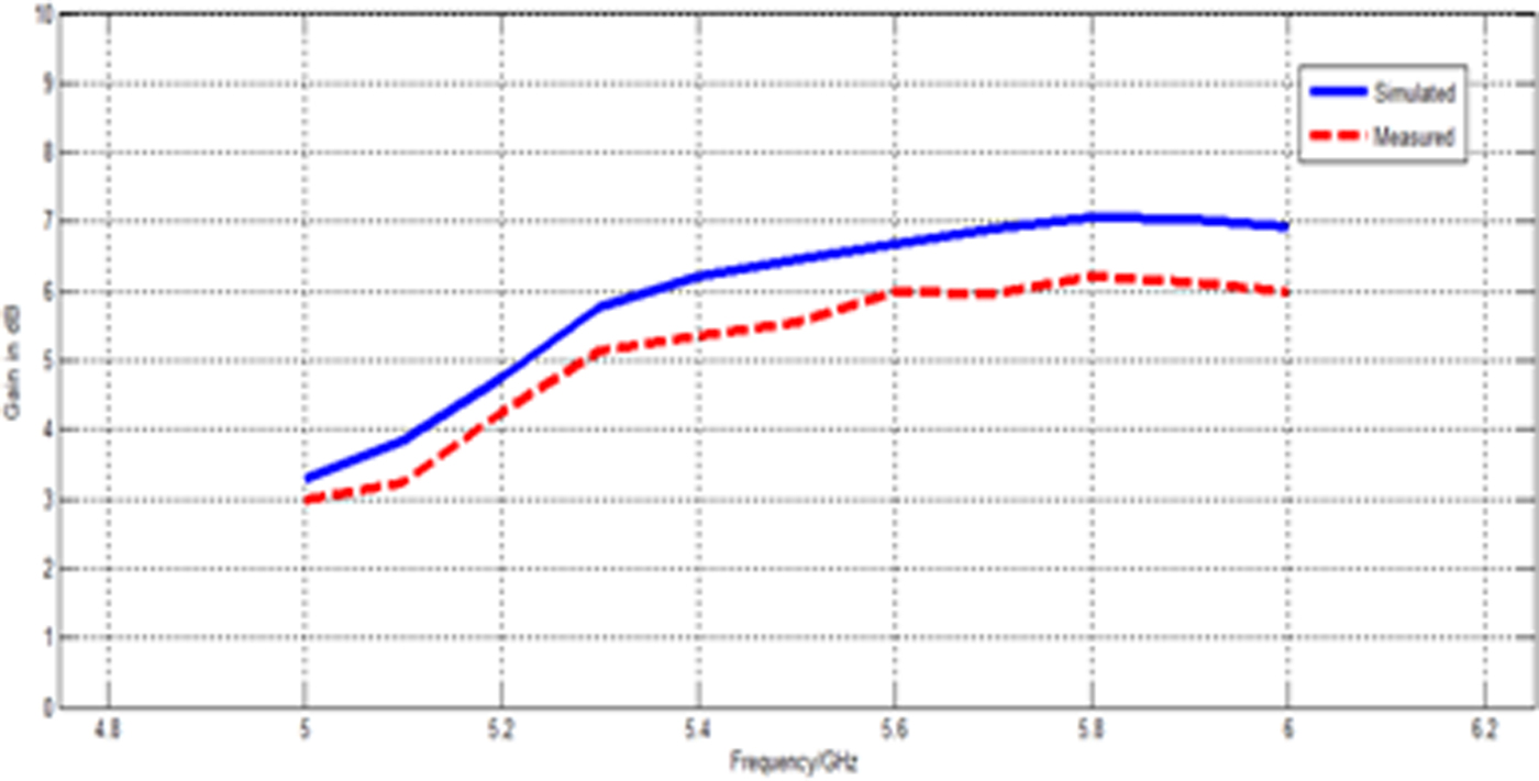
Fig. 16. The comparison of simulated and measured values of the antenna's gain.
V. CONCLUSION
In the current paper, an aperture coupled, complementary stacked (three-layered) MSA is presented for wireless applications of UWB from 5.28 to 5.85 GHz, IEEE802.11a/ WLAN from 5.15 to 5.35 GHz, a IEEE 802.11b/WLAN band from 5.75 to 5.85 GHz, UNII band from 5.25 to 5.825 GHz and WiMAX band from 5.25 to 5.85 GHz. The two patch antennas excite nearby frequencies leading a broadband behavior. The DGS that has a “π”-shaped slot in the ground plane helps in enhancing the operational bandwidth as it acts like an LC circuit whose frequency is chosen near the existing operational band of antenna. The antenna's feed network (matched to an impedance of 50 Ω) has a “T”-shaped feed line that parasitically couples power to the two complementary patch antennas using an aperture slot in the ground plane. The feed network is matched at a VSWR of 1.2 and also helps the antenna in radiation of circularly polarized fields. Apart from a compact size, circularly polarized nature of the antenna is an added advantage for it to be used in RF front end circuits and handheld devices, as the orientation of the antenna will not affect the system's performance by a large factor. Some complementary antennas have also been mentioned in the literature, but these antennas are basically stacked complex fractal geometries and show only a dual-band behavior [Reference Malik, Kalaria and Kartikeyan15]. The proposed antenna is a much simpler geometry with a better (UWB) performance and thus it is easier to implement with more wireless applications covered in a single antenna. This makes the antenna a preferred choice for the proposed RF applications.
In conclusion, the multilayered complementary geometry of the antenna with two resonating patch antennas and a DGS is responsible for allowing it to show a broadband behavior. The measured results closely match the simulated ones in terms of gain characteristics and impedance bandwidth and this makes the proposed antenna well suited for use in RF handheld devices in indoor wireless applications.
ACKNOWLEDGEMENTS
The authors are thankful to Dr. M.V. Kartikeyan, Professor Indian Institute of Technology, Roorkee for his kind help and the University Grants Commission (UGC) for providing the necessary resources for carrying out the research work. The UGC, New Delhi, India has provided a Fund grant of Rs. 15.8 lakhs under the major project scheme for setting up the anechoic chamber in the antenna testing laboratory at Thapar University, Patiala, India.
 Amanpreet Kaur was born in Udhampur (Jammu and Kashmir), India. She received her B.E. degree in Electronics and Communication Engineering from Jammu University in 2004. She got her M.E. degree in 2006 (specialization in Wireless communications) from Thapar University, Patiala, India. She joined Thapar University in 2006 as a Lecturer and is currently working there as an Assistant Professor .Her research interests include Wireless Communication systems (MIMO Systems) and microstrip antennas for wireless communication systems. She has handled projects worth Rs. 25 lakhs and is a life member of IETE (Institution of Electronics and Telecommunication Engineers). She has published 20 research papers in International journals and conferences and three publications in SCIE journals.
 Rajesh Khanna was born in Ambala, India. He received B.Sc. (Engg.) degree in Electronics & Communication in 1988 from Regional Engineering College, Kurkshetra and M.E degree in 1998 from Indian Institute of Sciences, Bangalore. He was with Hartron R&D center till 1993. Until 1999 he was in All India Radio as Assistant Station Engineer. Presently he is working as a Professor in the Department of Electronics & Communication at Thapar University, Patiala. He completed his Ph.D. degree in 2006. He has handled project worth Rs. 95 lakhs and is presently handling projects worth Rs. 70 lakhs, He has published 30 papers in International journals and 20 papers in International conferences. His area of interest includes wireless communication and antennas. He has guided around 55 ME thesis and nine Ph.D. theses. Dr. Khanna is a Fellow of the Institution of Electronics and Telecommunications Engineers (IETE) and life member of ISTE, Punjab Academy of Sciences.