


I. INTRODUCTION
Micro-electro-mechanical systems (MEMS) for RF application have been widely studied in the last decade. The extraordinary performances of RF MEMS in terms of loss, power consumption, and linearity have been largely proved in many applications such as re-configurable high-Q filters, phase shifters, and switching networks units [Reference Rebeiz1]. Nonetheless, the reliability of RF MEMS switches is still an open issue and many efforts have been done to acquire a better insight in the evolution of degradation, modes such as dielectric charging, contact deterioration, and power handling.
Recently the research has addressed the issue of long-term reliability, which is a fundamental requirement for redundancy networks of satellite system payloads. Some examples of redundancy networks can be found in [Reference Daneshmand and Mansour2], specifically designed for space applications. Redundancy switches typically have to be continuously biased for a very long time (i.e. 15 years) without any decay of electromechanical and electromagnetic performances. In addition, they are required to change quickly their state when the bias is removed. In particular, a long-term bias voltage may induce dielectric charging, eventually leading to the ON-state stiction of the movable membrane. Recent works [Reference Mardivirin3, Reference Tazzoli4] propose long-term actuation predictive models for dielectric charging, accounting also for the substrate material. The latter indeed has a not negligible impact on the dielectric charging mechanism especially in case of dielectric-less switches, where charging can still occur into the substrate and/or dielectric layers underneath the electrodes.
In some cases ON-state stiction can be avoided by optimizing the mechanical design in order to achieve a high self-restoring force of the MEMS membrane [Reference Nishijima, Hung and Rebeiz5]. However, this may be not enough to guarantee the switch functionality in case of very long bias time. An interesting idea is to use an active opening mechanism, such as the one reported in [Reference Sterner6]. In this case, a contact switch exploiting a bi-stable mechanism and a third bias electrode was proposed. Despite the potential effectiveness of a bi-stability device, its long-term reliability has not been fully characterized yet. The RF MEMS switch reported in [Reference Repchankova and Iannacci7] employs a thermal mechanism to actively restore the switch after the stiction.
The idea of a third electrode or pull-out (PO) electrode to actively control the position of the suspended membrane has been also proposed in [Reference Peroulis, Pacheco and Katehi8], where the PO electrode is realized on top of the bridge. However, this implies a more complex fabrication process and further electromagnetic parasitic effects to be considered. In [Reference Robin, Millet, Segueni and Buchaillot9], the PO electrode is placed at the same level of the pull-in (PI) electrode without introducing further process steps. In this case, a simply supported membrane is designed in order to provide high flexibility and large displacement capability. However no reliability tests have been reported yet to validate such a design for long-term actuation. Alternatively, a toggle or push–pull mechanism has been implemented in [Reference Simon10] by anchoring a cantilever by means of torsion springs. However high control of the stress gradient is required in the suspended structures in order to preserve their electro-mechanical performances.
This work presents the design, manufacturing, and characterization of a RF MEMS capacitive switch implementing an active push–pull restoring mechanism, and it is an extension of the work reported in [Reference Solazzi11]. Such a concept, based on a previouswork extensively described in [Reference Rangra12], exploits torsion anchor springs and a third electrode to mechanically restore the OFF-state of the switch in case of ON-state stiction. In Section II the proposed mechanism is largely described, reporting also the related finite element model. Section III briefly describes the manufacturing process, along with the electromechanical and electromagnetic performances. In Section IV, long-term stress characterization is also reported and discussed in detail,proving the effectiveness of such an anti-stiction mechanism in presence of dielectric charging.
II. DEVICE DESCRIPTION
A) Concept
Figure 1 shows the cross-sectional view of the MEMS switch employing the push/pull or toggle mechanism. The switch consists of a suspended membrane anchored to a fixed support by means of four torsion springs. The membrane is composed of different parts: a central part realizing the mobile plate of the variable capacitor, two mobile electrodes implementing the toggle mechanism, and two couples of levers connecting the central part and the mobile electrodes. The bridge can be pulled up or down by applying a voltage on two couples of fixed electrodes, which are symmetric with respect to the central RF line underneath the membrane. The couple of fixed electrodes closer to the RF line are referred to as PI electrodes, whereas the couple of fixed electrodes placed at the extremities of the membrane are called PO electrodes. In order to distinguish the toggle PI and PO active mechanisms from the PI and PO voltages of a standard switch configuration, the latter will be referred to as actuation and release voltages.

Fig. 1. Sketch illustrating the cross section of the device when (a) zero bias voltage is applied, (b) PI actuation, or (c) PO actuation occurs.
The mechanism works as follows. When V biasPI > 0 V and V biasPO = 0 V, the anchor springs start to torque, allowing the central part to move toward the underpass RF signal line, thus producing an increase of capacitance. The capacitance assumes its maximum value C ON (Fig. 1(b)) when V biasPI > V actPI. On the other hand, when V biasPO > 0 V and V biasPI = 0 V, the bridge central part starts moving upwards, lowering the device capacitance downto its minimum value C OFF, which is achieved when V biasPO > V actPO (Fig. 1(c)).
B) Model
The device was first designed following the analytical model described in [Reference Rangra12]. This step aimed at optimizing the membrane dimensions in order to have an actuation voltage around 60 V. Moreover, anchor springs could exhibit a tendency to bend downwards under high bias voltages, making the toggle mechanism ineffective. Therefore the springs should be as short as possible, so that their bending stiffness is maximized. The dimensions listed in Table 1 were chosen in order to satisfy these requirements, leading to a theoretical actuation voltage of about 57 V. In addition the proposed design allows the movable electrode to avoid the direct contact with the fixed electrodes after the snap down.
Table 1. Geometrical dimensions and material properties of the toggle switch.

Since the analytical model neglects some non-linearities such as the effect of residual stress in thin layers, a finite element method (FEM) simulation was performed by using ANSYS™Multiphysics [13]. A residual stress of σ0 = 50 MPa (typical value for the available fabrication process) was considered. FEM results confirmed that the anchor springs exhibit insignificant bending for V biasPI,PO = 80 V, as reported in Fig. 2.

Fig. 2. FEM displacement solution of the toggle switch for (a) PI and (b) PO actuation when V bias = 80 V is applied alternatively to PI and PO electrodes.
III. EXPERIMENTAL
A) Fabrication
A picture of the fabricated device is shown in Fig. 3. The toggle switch was manufactured on a high resistivity 525-µm thick silicon substrate by using the well-established 8-mask process of the FBK foundry [Reference Farinelli14]. The switch is integrated in a 50 Ω coplanar waveguide (CPW), and consists of a 720-µm long and 2-µm thick electroplated gold membrane anchored to CPW ground by means of four 30-µm long springs. The central part of the membrane and the movable electrodes are also reinforced by an additional 3.5-µm thick layer of electroplated gold for increased stiffness. The two couples of PI and PO electrodes are made of 0.63-µm thick polysilicon layer. The central part of the membrane is a 90-µm × 90-µm square suspended above 0.63-µm thick Ti/TiN/Al/Ti/TiN layer and 0.1-µm thick low temperature oxide underpass.

Fig. 3. Micrograph of the manufactured toggle switch with an indication of the most relevant geometrical parameters.
An experimental low-temperature release step was performed at the end of the manufacturing process in order to guarantee minimal stress gradient and high planarity of the gold membrane, as shown in Fig. 4 [Reference Mulloni15].

Fig. 4. Profile measurement of a realized device obtained with a Zygo Optical Profiler. (a) 3-D view and (b) longitudinal profile along the switch.
Mechanical stoppers are introduced under the movable electrodes, next to the fixed actuation electrodes. This allows for the removal of the insulating layer from the top of the fixed electrodes. Since some dielectric layer still surrounds the dielectric-less electrode, a certain amount of charge injected from the electrodes to such a dielectric layer (which in this case is thermal oxide) is expected. The effect of this charging is relevant especially for continuous long actuation [Reference Mardivirin3]. In addition, the mechanical stoppers are designed thicker than the underpass layer, so that a 0.1-µm air-gap is still present when the switch is ON. This allows for a repeatable C ON/C OFF ratio of about 12.
B) Characterization
The manufactured device was experimentally characterized to evaluate its electromechanical and electromagnetic properties. First of all PI–PO actuation voltages and mechanical resonance were measured as a further validation of the FEM model. The mechanical resonant frequency was measured by means of the Laser Doppler Vibrometer integrated into a Polytec MSA-500 optical profilometer. The comparison between simulations and measurements showed excellent agreement, as reported in Table 2.
Table 2. Mechanical properties of the toggle switch.
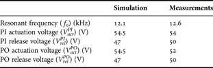
Figure 5 presents the equivalent circuit model. In case of the toggle switch, C ON is the capacitance assumed at the PI actuation, whereas C OFF is the value of the capacitance at the PO actuation. Moreover, if C 0 is the capacitance value when no bias is applied to either the PI or PO electrodes, C OFF is lower than C 0 by design, allowing for an enhanced capacitance ratio C r = C ON/C OFF.

Fig. 5. Equivalent lumped circuit of the toggle switch.
S-parameter measurements were performed from 0.1 to 40 GHz showing insertion loss better than 0.5 dB and return loss better than 15 dB over the whole frequency range. In the ON state the switch presents an isolation of about 10 dB at 40 GHz corresponding to a C ON/C OFF ratio of 12, which is in a good agreement with the theoretical one. The stopping pillars placed on the actuation electrodes indeed prevent the toggle central part to fully contact the RF line underneath, and consequently high values of C ON cannot be reached. On the other hand, this allows for a very predictable and repeatable C ON since the latter is not sensitive to dielectric roughness, bridge shape factors or applied voltage.
Figure 6 reports OFF and ON state S-parameter measurements and the corresponding fitting, which allowed for the extraction of the circuit element values reported in Table 3. The adopted circuital model does not account for the transmission line impedance variation in correspondence of the MEMS membrane due to the larger CPW slot width, which is needed to pattern the PI and PO electrodes. This cause a slight mismatch between the equivalent and measured return loss around 20 GHz, even though the envelopes of the two curves are pretty similar in the entire 0.1–40 GHz frequency band. This allows also for the usage of the simple equivalent circuit reported (Fig. 5) to model with pretty high accuracy the capacitance variation for different values of PI/PO bias voltages [Reference Farinelli16].

Fig. 6. S-parameters measurements (continuous line) and circuit simulations (dashed line) for the OFF (a) and ON (b) state of the toggle switch.
Table 3. Electromagnetic properties of the toggle switch.

IV. LONG-TERM RELIABILITY
The long-term reliability of the switch was analyzed by keeping the toggle switch ON for a considerable amount of time. Then the effect of the dielectric charging on the whole switch operation is evaluated by monitoring the evolution of the electromechanical and electromagnetic properties during the test. For this purpose the measurement setup depicted in Fig. 7(a) was employed. The setup is based on a Hp 8753E Vector Network Analyzer and a dual channel Keithley 2612 source meter, which allows for a simultaneous control of PI and PO electrodes. The control waveforms utilized for the test are represented in Fig. 7(b) for clarity.

Fig. 7. (a) Schematic of the measurement setup employed for long-term performance evaluation of the switches under test, and (b) resulting waveforms applied to the PI and PO electrodes to monitor the S-parameters evolution at 6 GHz.
A continuous stress voltage of 80 V is provided to PI electrodes for increasingly longer time intervals t i (from few seconds up to ~1 h). Meanwhile, PO electrodes are biased at 0 V. After the stress interval, a t s-long triangular voltage waveform is applied to the PI electrodes, sweeping from 0 to 80 V, and then back to −80 and 0 V. Immediately after, the same waveform is applied to the PO electrodes, keeping the PI electrodes at 0 V. This procedure is then repeated for a longer time t i+1. During the sweep time t s the Vector Network Analyzer acquires the S-parameters at selected sample intervals, constantly applying a 6 GHz, 0 dBm RF signal at the switch input port.
As a result, for t s < < t i this procedure guarantees the simultaneous evaluation of the PI (V actPI, V relPI) and PO (V actPO, V relPO) voltages, by monitoring the S-parameters evolution at 6 GHz with respect to the test time. As expected, the PI actuation voltage decreases in time since the electrodes under stress inject charges into the substrate.
After about 6 h 36 min, the switch is stuck in down position. Nevertheless, after the application of a voltage sweep on the PO electrodes, the membrane is able to release and assumes again its up-state position (Fig. 8(a)), even if charges still remain on the substrate underneath the PI electrodes. Moreover, the OFF state capacitance C OFF remains mostly constant over the same time range (Fig. 8(b)), ensuring also constant long-term switch performances even in presence of dielectric charging. Figure 8(b) shows also a decrease of the ON state capacitance, which was unexpected. This is probably due to some mechanical deformations of the membrane induced by the pressing of the mobile electrodes on thestoppers. However, the capacitance ratio C r experiments just a slight change of about 10% of its value at t = 0 s.

Fig. 8. Long-term reliability results: (a) evolution of actuation (o) and release (Δ) voltages for PI (black) and PO (gray) electrodes, and (b) evolution of ON (black) and OFF (gray) capacitances and capacitance ratio (blue) over stress time. Note that in case of ON-state stiction, the sweep on PO electrodes allows the switch to restore the OFF position.
The effectiveness of the toggle mechanism can be proved empirically for periods of time longer than 10 hours (i.e. the test duration) by extrapolating the trend of actuation and release voltages over time. Thus the voltage shifts ΔV xPI(t) = |V xPI(t) − V xPI(0)| and ΔV xPO(t) = |V xPO(t) − V xPO(0)| are calculated and fitted by the following power law [Reference Mardivirin3]:
where the subscript x stands for act (actuation) or rel (release), and the superscript γ stands for PI or PO.
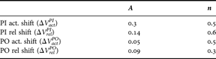
Figure 9 shows the log–log scale plot of PI–PO voltage shifts evolution versus time and the corresponding fitting curves. The data points measured in the first 10 s have not been considered since the corresponding stress intervals were comparable with the sweep time t s. The extracted fitting parameters A and n are reported in Table 4 for all cases. The PI release trend provides information about the temporary ON-state stiction. In this case, the best fit values for A and n are 0.14 and 0.6, respectively. Thus ON-state stiction is estimated to occur at a time t f,ON, which can be calculated from equation (1) when ΔV relPI(t f,ON) = V relPI(0) as follows:
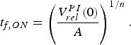
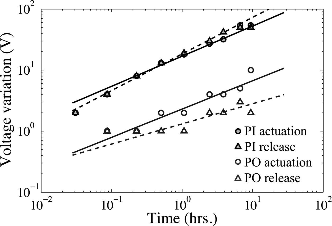
Fig. 9. Evolution of actuation (o) and release (Δ) voltage shifts for PI (black) and PO (gray) electrodes.
Table 4. Voltage shift fitting parameters.
By using the values of A and n found for the PI release, t f,ON is found to be approximatively 6 h, as also observed previously.
For a switch in standard configuration (i.e. without PO mechanism), the estimated value of t f,ON represents the time-to-failure at which the membrane is no longer able to change its status through the mechanical restoring force of the anchor springs. Conversely, in the toggle switch the total restoring force can be increased by the bias voltage provided at the PO electrodes, thus the upper lifetime limit of the switch depends no longer on the PI release shift but on the PO actuation shift. According to Fig. 9, PO actuation voltage shift follows qualitatively the same trend as the PI actuation/release shift, with n = 0.5. However, A is equal to 0.3 and 0.05 for PI and PO actuation, respectively. This implies that PO actuation shift is scaled by a factor 0.3/0.05 = 6 with respect to the PI actuation shift. On the other hand, the PO release evolution is not easy to evaluate since the related voltage shift is comparable with the voltage sweep step (≈1 V).
The switch effectively fails working when the bias voltage provided to PO electrodes is not enough to recover the stuck membrane, and this happens for ΔV actPO(t f,eff) = V biasPO − V actPO(0), where t f,eff is the effective switch time-to-failure. As a result, supposing that the PO actuation shift preserves the same trend after the ON-state stiction of the membrane, for V biasPO = 80 V t f,eff can be calculated as

By utilizing A and n extracted from the PO actuation, the effective time-to-failure is around 180 h. Therefore the switch lifetime is improved by a factor of ~30 because of the toggle mechanism. Note that however this calculation supposes that the charging mechanism at the PI electrodes is following the exponential law for ever, i.e. no saturation effects are present. In real case we can expect that at a certain time the charging effect reaches a saturation level and the corresponding down-state electric force becomes almost constant. Once this force will be known, the toggle switch can be designed so to have a PO force larger than the charging force at the PI and consequently being able to recover the switch at any time. Long-term measurements to validate such hypothesis are on-going.
V. CONCLUSION
An active push/pull toggle RF MEMS switch suitable for redundancy network applications has been presented in this work. The electromechanical properties and electromagnetic model have been presented and compared with experimental data, showing excellent agreement. A long-term characterization under continuous voltage stress was also reported, demonstrating the effectiveness of the proposed mechanism for the recovering of the switch OFF status in case of stiction caused by dielectric charging at the ON state. Results showed also that the switch capacitance ratio remains quite constant over time. Thus, even if stiction occurs at the ON state, the switch cannot be considered in failure state as long as the PO electrodes are able to recover the OFF state. The proposed predictive model shows that the switch lifetime may be improved by a factor 30 by means of the toggle mechanism.
ACKNOWLEDGEMENTS
This work was partially supported by the European Space Agency under Contract No. ITT AO/1-5288/06/NL/GLC and by ENIAC project END “Models, Solutions, Methods and Tools for Energy-Aware Design”ENIAC JU GA n.120214.
 Francesco Solazzi (IEEE Student Member) was born in Assisi, Italy, in 1983. He graduated in Electronic Engineering at University of Perugia, Italy, in 2007, and he got his Ph.D. degree in Information and Telecommunications Engineering from Universityof Trento, Italy, in 2011. Since November 2007 he has been in Fondazione Bruno Kessler, (FBK), Trento, Italy, working on the design and characterization of high-reliability RF MEMS switches for space applications. From September 2009 to August 2010 he was at the Compound Semiconductor Technology Lab. at Lehigh University (PA, USA), as a visiting pre-doctoral researcher, working on the RF MEMS analysis and design for high-power applications. His research interests include the electromagnetic and electromechanical design and characterization of RF MEMS switches and resonators.
 Augusto Tazzoli (IEEE Member) was born in Padova, Italy, in 1978. He graduated in Electronics Engineering at the University of Padova in 2003, and he received the Ph.D. degree in Electronics and Telecommunications Engineering from the same University in 2006 working on the reliability of silicon, compound and MEMS devices. From January 2007 to January 2010 he was post-doc at University of Padova, working on the development of measurement systems in genre, Transmission Line Pulser systems, ElectroStatic Discharge phenomena, solid state lighting, compound semiconductors, HV pulse generator, and RF-MEMS. He currently holds a researcher associate position at the Department of Electrical and Systems Engineering, University of Pennsylvania, Philadelphia, PA, USA, working on Micro and Nano Electromechanical Systems, oscillators, phase-noise reduction techniques, and reliability in genre. In his career he has coauthored about 100 papers, awarded with three best paper awards. He serves as reviewer of several International Journals and in Symposia TPCs.
 Paola Farinelli was born in Assisi, Italy, on September 19, 1978. She received the Laurea degree (with distinction) in electronic engineering from the University of Perugia, Italy, in 2002. In 2002 she joined the Department of Electronic and Information Engineering of the University of Perugia as a Ph.D. student. In 2003 she conducted research work at the “Institut de Recherche en Communications Optiques at Microondes (IRCOM)”, Limoges University, (France). From November 2004 to May 2005 she has been a visiting researcher at VTT Millilab (Finland). In January 2006 she received the Ph.D. degree and she is currently working at the University of Perugia as a contract researcher. Her research activity includes the electromagnetic modeling and design of reconfigurable RF MEMS devices such as SPDT switches, phase shifters, power dividers, filters.
 Alessandro Faes received his degree in material engineering from the University of Trento, Italy, in 1999 and his Ph.D. degree from the same University in 2003, with a thesis on MEMS silicon condenser microphones. Starting from 2003 he worked on MEMS ultrasonic sensors for object detection as a post-doctoral fellow at the Center for Scientific and Technological Research ITC-irst. In 2006 he joined Zobele Group, where he worked as innovation project manager. In 2008 he joined the MEMS Research Unit at FBK. His current research interests include RF-MEMS switches and capacitive microphones.
 Viviana Mulloni graduated at the University of Padova in 1993 and received her Ph.D. degree in physical chemistry in 1997 from the same University. In 1997 was at Northwestern University (IL, USA) as a post-doc fellow and at the beginning of 1998 joined the Physics Department of the University of Trento, working on fabrication and optical characterization of porous silicon and nanocrystalline silicon devices. In 2003, she started working on MEMS devices at FBK, getting involved mainly in RF-switch fabrication and characterization. Her current research interest includes micro-electromechanical systems and several selected topics on material science.
 Benno Margesin received the his doctor degree in physics from the University of Bologna, Italy, in 1980. From 1982 to 1985 he was involved in the development of heavy ion sources and heavy ion implanters at the ITC-irst Material Science Division. In 1986 he joined the Integrated Circuit Laboratory at former ITC-irst where he worked on the development of low-temperature microcalorimeters and mixed ISFET/CMOS chemical sensors. Since 1997 he heads the Micromechanics Group of FBK-irst and since the beginning of 2008 he is responsible for the MEMS Research Unit of FBK. Currently, he is involved in the development of RF-MEM switches for space applications, Microwave filters, capacitive microphones, and bolometer arrays.
 Gaudenzio Meneghesso (IEEE S ’95 – M ’97 – SM ’07) graduated in Electronics Engineering at the University of Padova in 1992 working on the failure mechanism induced by hot-electrons in MESFETs and HEMTs. He received the Italian Telecom award for histhesis work in 1993. In 1997 he received the Ph.D. degree in Electrical and Telecommunication Engineering from the University of Padova working on hot-electron characterization, effects and reliability of GaAs-based and InP-based HEMTs and pseudomorphic HEMTs. Since 2011 is with University of Padova as Full Professor. His research interests are: (a) electrical characterization, modeling and reliability of microwave and optoelectronics devices on III–V semiconductors such as GaAs, InP, SiC, and GaN; (b) electrical characterization, modeling and reliability of RF-MEMS switches for reconfigurable antenna switches; (c) design, characterization, and modeling of electrostatic discharge (ESD) protection structures for CMOS and SMART POWER integrated circuits including ElectroMagnetic interference issues; and (d) characterization and reliability of organic semiconductors devices. Within these activities he published more than 400 technical papers (of which more than 50, invited papers and 6 best paper awards at 1996, 1999, 2007 and 2009 ESREF Conferences, and at the 2006 EOS/ESD Symposium). He is reviewer of several international journals. He served several years for the IEEE-International Electron Device Meeting (IEDM): he was in the Quantum Electronics and Compound Semiconductors sub-committee as a member in 2003, as chair in 2004 and 2005 while in 2006 and 2007 he has been in the Executive Committee as European Arrangements Chair. He is serving since 2005 in the TPC of the IEEE International Reliability Physics (IRPS) Symposium (being TPC Chair of the Compound Semiconductor from 2008 to 2010) and since 2009 he is with the management committee. He is in the steering committee of several international conferences: ESSDERC, ESREF, HETECH, WOCSDICE, TWHM. Currently, he is Associate Editor of the IEEE Electron Device Letter for the compound semiconductor devices area since 2007.


