I. INTRODUCTION
Radio frequency (RF) and microwave power amplifiers (PAs) are key technologies for wireless systems [Reference Raab Frederick1] as well as for particle accelerators [Reference Giacomo Marco2]. Owing to the overlap of the frequency regime of these two fields, research efforts for this technology are equally useful. Nevertheless for the former, it is typically the amplifier's linearity, output power, and efficiency that drive the system's performance, power budget, and thermal design. For RF systems of particle accelerators [Reference Valuch3], features like phase noise, system efficiency, minimum trips, and modular/scalable architecture are important for quality, stability, and high lifetime of particle beam. RF and microwave amplifiers based on vacuum-tube technology are widely used in these applications due to their high-power capability and established flight history. However, motivated by benefits such as low supply voltage, slow degradation, low research cost, and a wide commercial technology base, there is considerable interest in developing efficient, solid-state power amplifiers (SSPAs) [Reference Ulf, Rolf, Se'bastien, Kristina and Martin4] as an alternative to vacuum tube-based systems. Their price, performance, and reliability are quite likely to improve [Reference Heid and Hughes5] with the evolution of wideband gap semiconductor-based devices [Reference Kuhn6] and growing demand in particle accelerators. In fact, many institutes like Soleil [Reference Marchand, Lopes, Ribeiro and Ruan7], European Synchrotron Radiation Facility (ESRF) [Reference Jacob, Mercier, Langlois and Gautier8], Raja Ramanna Centre for Advanced Technology (RRCAT) [Reference Hannurkar9], and Advanced Photon Source (APS) [Reference Popovic and Waldschmidt10] have developed such sources or are replacing their vacuum tube-based RF power source. Along with getting clean RF and Microwave (RFM) power (free from phase noise and spurious) solid-state device failure rate reported from Soleil synchrotron is 3% per year including infant mortality.
In this paper, design methodology of 50 kW SSPA at 505.8 MHz is described along with characterization at component level as well as system level. It is designed for the RF system [Reference Hannurkar11] of Indus-2 synchrotron radiation source. The Indus Accelerator complex [Reference Singh12] at RRCAT consists of Indus-1 (a 100 mA, 450 MeV storage ring) and Indus-2 (a 2.5 GeV storage ring), sharing a common injector system, comprising of 20 MeV microtron and 700 MeV booster synchrotron.
As the power output of Laterally Diffused Metal Oxide Semiconductor (LDMOS) devices is limited, a large number of PA modules are paralleled for making this kW-level amplifier [Reference Akhilesh, Sharma, Gupta and Hannurkar13] with the help of power dividers and power combiners. Amplifier architecture relies upon signal splitting, amplification and summing strategy. In order to make modular, scalable, and reliable systems, a combination of multi-way and corporate scheme is used for power summing or combining. Combiner topology is influenced by efficiency, low phase noise, reliability together with economic issues, and size constraints. PAs, which are main gain blocks, need to be designed with least variation in their output signals from a mean value, for maximum possible combining efficiency. In practice, for circuit-level combining there is some variation due to fabrication tolerances, cable connection, and impedance tuning of PAs. Among amplitude and phase variations, the latter is the dominant factor for efficiency degradation as long as variations in amplitude have zero mean [Reference York14]. SSPA designers have tried different methods like phase-delay line [Reference Diop, Ruan, Lopes, Polin, Ribeiro and Marchand15] and forced compression of drain characteristics [Reference Gaspar, Pedrozzi, Ferreira and Garvey16] to minimize variation in amplitude and phase of PAs. In the present endeavor a tight control was maintained for this variation by selecting a suitable combiner structure and a PA impedance matching circuit. In combiners, the absence of isolation resistor or moving/planer parts adds toward signal symmetry and reduced system trips. A multi-way unit radial slab-line topology with electrical symmetric structure gives nearly no variation in phase/amplitude with combining efficiency approaching 98%. PA modules with semi-rigid coaxial line transformers and minimum tuning elements give repeatable performance. Experimental characterization verifies the suitability of this design for addressing phase and amplitude errors' problem.
II. 50 kW AMPLIFIER DESIGN DESCRIPTION
In order to meet RF power demand and specific requirements encountered in Indus-2 particle accelerator, an architecture based on combination of circuit-level corporate and radial power dividing–combining approach was selected for the 50 kW SSPA. As scalability, modularity, and reliability were the key metrics of this architecture, a generic template in the form of a 13-kW amplifier unit was designed to achieve target power by its repetition and corporate power combining. For 50 kW power, four such units were incorporated in a two stages binary tree with two-port combiners, capable of handling power up to 45 and 65 kW, respectively. This scheme is shown in a simplified manner in Fig. 1 along with estimated gain and power calculation at each junction of the chain.

Fig. 1. RF architecture and gain/power calculation for 50 kW SSPA.
In this scheme an eight-port divider feeds the RF signal to each of the four 13 kW units. Half of the branch ports of this divider, presently terminated in matched load, are for future expansion. Phase shifters inserted in used branch ports adjust real-time operational phase difference for each unit. Different directional couplers (not shown in the figure) are used to sample RF power at various junctions of this SSPA. Such system allows easy serviceability and expandability with similar mechanical footprint and peripheral connections even for different frequency selection.
Each of the 13 kW units, designed for this scheme, includes water cooling, Field Programmable Gate Array (FPGA)-based protection and monitoring system apart from PA modules, dividers, combiners, and directional couplers, all housed in a standardized Euro chassis. As seen in Fig. 2, showing simplified RF hardware of this unit, 32 PAs (each one at 500 W) are power combined in two stages. In the first stage there are two similar groups each one consisting of a 16-port radial divider, 16 PAs, and a 16-port radial combiner. In the second stage, outputs from two such groups are combined with the help of a two-port combiner to get the required 13 kW power. A low-power directional coupler is inserted between the output of each PA and the input of 16-port combiner monitor forward and reflected RF component. Every 500 W PA module is individually powered by a compact switched-mode power supply (SMPS) capable of delivering 20 A at 50 V DC with a three-phase AC input.

Fig. 2. RF hardware scheme for 13 kW solid-state RF amplifier unit.
For data acquisition, each unit together with its interlocks forms an independent system with its own supervisory system performed by a graphical code developed in-house [Reference Sharma, Gupta, Akhilesh and Hannurkar17] using LabView™ RT. All of the PAs, with the help of the 1 kW coupler connected externally at output, provide a rectified sample of forward and reflected power to FPGA-based CRio analogue modules from National Instruments™. The whole system works as a distributed system over a TCP/IP network where all 13 kW units function independently and are centrally coordinated by a master PC. The system can be easily expanded by adding new members to this network. A 20 kW directional coupler is used to sample RF power of this 13 kW unit. Each unit occupies 1 × 1.2 m2 floor space and has 2 m height. Design description of different building blocks of this SSPA is presented below.
A) The RF amplifier module
For PA design BLF 573 LDMOS was selected as the workhorse on the basis of circuit simulation studies, carried out in Microwave Office™. Important design specifications of this PA are listed in Table 1.
Table 1. Specification of 500 W RF power modules.

Target power of 500 W was obtained by two such devices, each one designed for class AB with similar impedance matching and bias circuits, all on the same board. Using power match condition and impedance matching theory [Reference Cripps Steve18] gate and drain side impedances (both are having real part less than 2 Ω) were matched to system impedance of 50 Ω with the help of coaxial transformers and L section of lumped capacitors and microstrip line as seen in Fig. 3. Parallel RF operation of these two amplifying circuits was achieved with the help of on-board Wilkinson divider and combiner. The harmonic balance power analysis [Reference Vendelin George, Pavio Anthony and Rohde Ulrich19] and simulation were performed under desired source/load impedances to fine tune the PA circuit. A 500-W circulator, placed before the final output, protected the RF devices from reflected power.

Fig. 3. Impedance matching circuit for one half of the 500 W power module.
Five such PAs were mounted directly on a water-cooled copper plate. For improved heat transfer, LDMOS devices were bolted directly to this plate by applying a thin layer of silicone oil-based thermal compound. Fig. 4 shows a sketch of this cold plate and inner view of one of the PA modules. The data logging parameters acquired from each module are output forward and reflect power and cold plate temperature.

Fig. 4. PA module cold plate with inner view of PA module.
Fig. 5 summarizes RF performance for a typically designed PA. Power transfer characteristic is linear. Efficiency is lower than the calculated value by nearly 2%. Phase spread or AM–PM conversion factor is quite low. 1 dB bandwidth measured for this PA was 10 MHz. Harmonics and spurious components were −35 dBc.

Fig. 5. Measured gain and efficiency of 500 W PA module.
B) Rigid coaxial passive components
Owing to divide and sum strategy used in SSPA configuration, power dividers, combiners, and directional couplers directly affect final output power and efficiency. Different passive components, as detailed below, have been designed for the 50 kW SSPA. Realized with good mechanical and thermal design, these structures provide an excellent electrical symmetry for power combiners thus improving their amplitude and phase stability. Absence of isolation resistor and planer circuit (microstrip/strip line) in these components makes them attractive for high power and reliable performance, which otherwise may deteriorate due to heat dissipation, aging, and mechanical difficulty in placing the resistor inside the structure.
1) POWER DIVIDERS AND COMBINERS
Two-port in-phase combiners required at different stages are junction of rigid coaxial lines suitably matched at combined port. Instead of Wilkinson-type quarter-wave sections, they make use of cascaded coaxial lines for impedance matching, resulting in overall compact structure. On the other hand, the 16-port divider/combiner has N input coaxial ports symmetrically spaced along the circumference of a parallel rigid-slab type radial line with output power extracted from the center, suitably matched to system impedance. A similar structure acts as a power divider with the roles of the feed port and the branch ports reversed. The designed structures are shown in Fig. 6.

Fig. 6. Two-port combiners (a) and 16-port radial combiner (b).
For combining N sources, radial power combiners [Reference Fathy20] offer a superior approach with efficient, reliable, and high-power output in compact housing. Design methodology of radial combiner [Reference Akhilesh, Sharma, Gupta and Hannurkar21] includes computation of relative input impedance Z′(r) and real value of characteristic impedance of radial line at radius r for dominant E mode. This methodology together with full-wave analysis in HFSS™ results in accurate prediction for the operating parameters and optimization of the electromagnetic structure.
All these designed structures were qualified after rigorous RF measurements. Measured return loss and power combining ratio or coupling for these combiners (Fig. 7(a)) conform to the calculated values. Comparison of HFSS result and measured isolation among branch ports for 16-port combiner is given in Fig. 7(b). Insertion loss for 16-port combiner is less than 0.1 dB corresponding to a combining efficiency of 98%.

Fig. 7. (a) Measured return loss and coupling for power combiners and (b) computed and measured isolation of 16-port combiner.
Imbalance in forward transmission coefficient from feed port to branch port, as seen in Fig. 8 is less than 0.2 dB in amplitude and nearly 2° in phase.

Fig. 8. Forward transmission coefficient of 16-port radial combiner.
All these measured data with minimum ripple in amplitude and phase prove the worthiness of the design methodology. It allows repeatable design and minimum loss in the system due to mismatch/reflection at various junctions of the SSPA.
2) DIRECTIONAL COUPLERS
For directional sampling and measurement of high-power RF signal coaxial directional couplers are the reliable high-power solution. Coupler structures at different power, designed for present application, are coaxial type with rectangular cross section. The coupling mechanism is similar to the one suggested by Tepatti et al. [Reference Valeria, Michele, Andrea, Augusto and Giovanni22]. Energy from longitudinal symmetric main line to auxiliary coaxial line is coupled using an aperture cut in a thin metal diaphragm. Each line has an outer conductor with a square cross section and a cylindrical inner conductor. The aperture shape corresponds to the desired longitudinal profile of the coupling factor. The necessary analysis, carried out in parts for longitudinal and transversal problems, provide the coupling factor and the characteristic impedances as functions of the structure dimensions. For transversal part, use of even and odd mode impedances (Z oe and Z oo [Reference Cristal23] was made for such uniformly coupled asymmetric lines.
 $$k\lpar z\rpar = \displaystyle{{Z_{oe} \lpar z\rpar - Z_{oo} \lpar z\rpar } \over {Z_{oe} \lpar z\rpar - Z_{oo} \lpar z\rpar }}$$
Here, k(z) is the coupling factor. The longitudinal design procedure adopted was based on the following equations [Reference Arndt24]:
 $$A_{13} = j2\pi \displaystyle{l \over \lambda }\int_0^l {k\lpar z\rpar {\rm e}^{ - 4\pi \lpar l/\lambda \rpar z} } \, {\rm d}z$$
Here, A 13 is voltage coupling from main port to coupled port, l is the length of the coupler, and λ is the wavelength. With proper choice of various dimensions, final design was carried out using structure simulator. Using this approach, three types of wide band (300–700 MHz) couplers have been built and characterized for maximum forward power of 1, 20, and 65 kW, respectively. Two such couplers are shown in Fig. 9.

Fig. 9. 1 kW and 65 kW directional couplers.
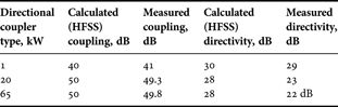
Measured insertion loss for all of these couplers is less than 0.05 dB whereas return loss is better than 28 dB at center frequency. Measurement results show very good agreement with the design specifications and electromagnetic simulations as compared in Table 2.
Table 2. Coupling and directivity of three types of designed directional couplers.
III. 50 kW AMPLIFIER: COMPLETE SYSTEM
50 kW SSPA (Fig. 10) completed with RF and ancillary components was commissioned and interfaced with Indus-2 SRS RF cavity resonator after being tested with a matched 80 kW RF water-cooled load. Presently, a high-power circulator is placed for the safety of this amplifier from the reflection generated at the RF cavity during beam injection and ramping. This amplifier is complete in all respects of safety interlock, water cooling, and power supply. Panel PC provides a GUI for all user related controls and indicators. An independent low conductivity water (LCW) plant capable of delivering up to 1200 l/m at a maximum pressure of 8 bar was used in the Indus-2 SSPA RF area. The supervisory and the interlock systems were tested in advance. The directional couplers were characterized in situ at high power. Measurements of output power, gain, and efficiency were performed for each of the 13 kW units individually followed by same measurement for complete 50 kW SSPA.

Fig. 10. 50 kW solid-state amplifier.
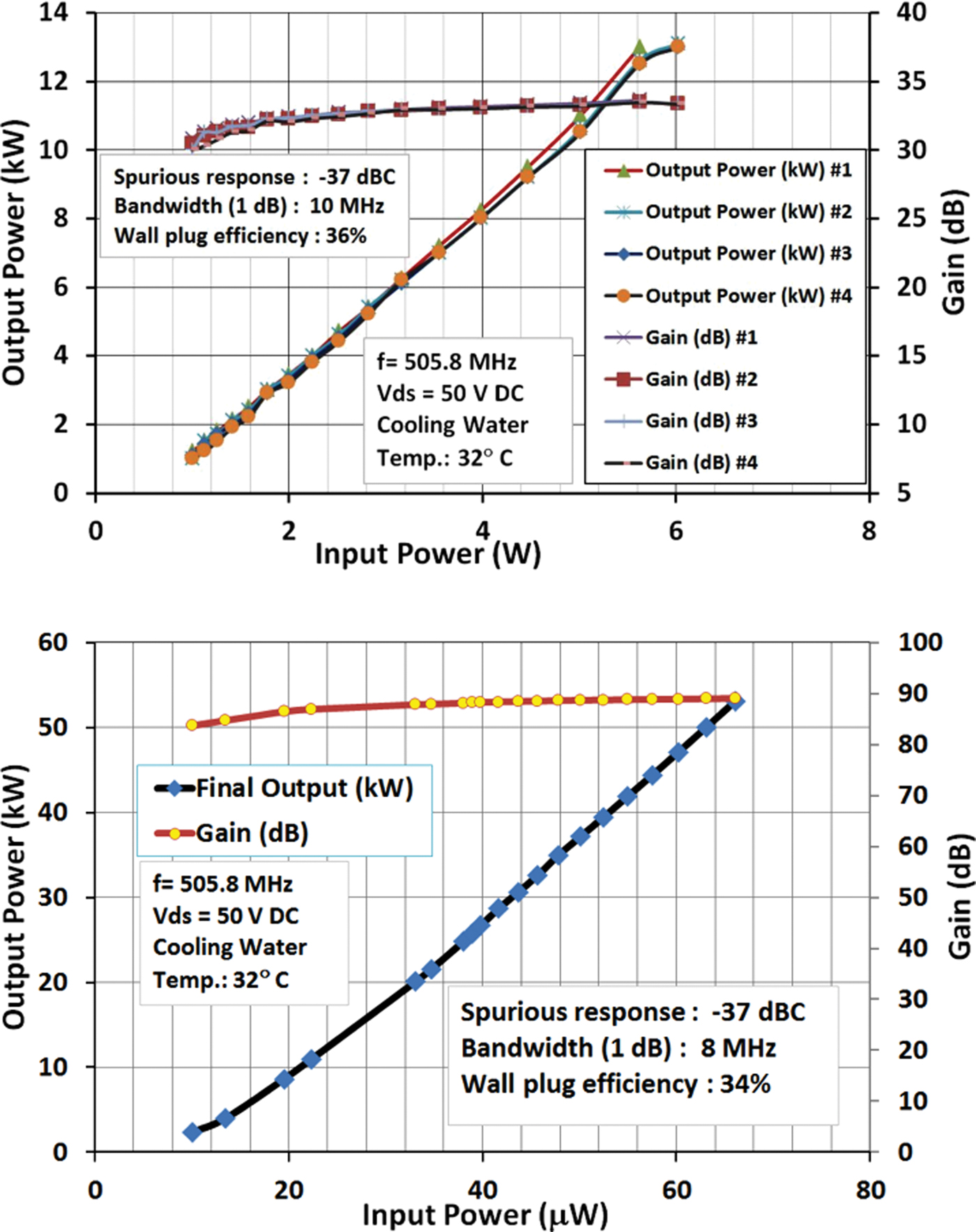
This characterization data of 13 kW units and this amplifier are shown in Fig. 11. There is a minor deviation in power characteristics of all four 13 kW units. This helps in achieving the best possible efficiency at corporate combining stage. For all amplifiers the characteristic is linear in common operation region. For 13 kW SSPA one dB compression point is beyond 12.5 kW. Average gain of 50 kW SSPA is 88 dB whereas 1-dB gain compression point is beyond 52 kW output power.

Fig. 11. Measured power transfer characteristics of 13 kW units (#1 to #4) and 50 kW SSPA at 505.8 MHz.
Thermography check-up of the PA modules showed that at maximum power, temperatures in the modules (near drain of LDMOS) can reach up to 95°C. Fig. 12 shows Infra Red (IR) image with maximum temperature of capacitor near drain side.

Fig. 12. IR image showing maximum temperature on drain side of one of the devices.
IV. CONCLUSION
At 505.8 MHz, a modular and scalable 50 kW solid-state RF amplifier was successfully designed and characterized for use with Indus-2 synchrotron radiation source. This amplifier make use of divide and sum strategy using 50 V LDMOS-based 500 W amplifier module, power combiner, divider, directional coupler, and FPGA-based control and interlock. With proper design of these modules and rigid structure RF components, amplitude and phase imbalance could be managed to a satisfactory level. The measured and predicted results are in good agreement. Successful development and characterization of this amplifier adds confidence for future development for selecting solid-state RF source, among other tube-based sources.
ACKNOWLEDGEMENT
We are thankful to members of the RF systems division for their contribution in the development of high-power solid-state RF amplifiers. Thanks are also due to members of the Indus accelerator team for their participation in Indus-2 operation with deployment of these amplifiers.
 Akhilesh Jain received B.E. in Electronics and Communication engineering from Vikram University in 1991 and M.Tech. in Microwave Engineering from Indian Institute of Technology, Kanpur in 1994. He joined Raja Ramanna Centre for Advanced Technology (RRCAT), Indore in 1994. Since then he is engaged in research and development of high-power solid-state RF amplifier and related components.
 P.R. Hannurkar received his B.E. in Electronics and Telecommunication from College of Engineering, Pune. He served as a Scientific Officer at Bhabha Atomic Research Centre (BARC), Mumbai, after graduating from the 20th batch of BARC Training School. Since 1986 he is leading RF and microwave activities for various particle accelerators in RRCAT.
 Deepak Kumar Sharma completed his B.E. (Bachelor of Engg.) from RGTU (Rajiv Gandhi Technical University) India. After completing his graduation in Electronics Engineering, joined the orientation course on advanced technologies and was appointed as a scientific officer in RRCAT. Since then he is working in the field of high-power solid-state RF amplifiers for various particle accelerator applications.
 Alok Gupta completed his M.Tech from the Department of Electrical Engineering, Indian Institute of Technology, Kanpur in 2005. Since then he is posted as a scientific officer at RRCAT under Department of Atomic Energy, India. His main areas of interest are RF amplifier, power combiners, directional couplers, and high-power rigid line components.
 Dr. Ashish Kumar Tiwari received the degrees of M.Tech. in Microwave Electronics from Delhi University, India and Ph.D. from Jadavpur University, Kolkata, India in 2008. Presently, he is a scientific officer in RRCAT. His research interest includes solid-state amplifiers, computational electromagnetic antennas, and vacuum electron devices.
 Mahendra Lad completed his B.E. in (Electronics and Telecommunication) from Devi Ahilya University, Indore in 1986. He joined RRCAT in 1987 as a scientific officer. Since then he is involved in RF system development for Synchrotron Radiation Sources at the center.
 Ramesh Kumar did B.Sc. (Engineering) in Mechanical from Ranchi University in 1989. He joined Bhabha Atomic Research Centre, Mumbai in 1991 as a scientific officer. Presently, he is involved in the development of coaxial and waveguide-based transmission line systems for RF system of accelerators at RRCAT.
 Dr. P.D. Gupta is Director, RRCAT. He is steering R&D programmers in several frontline areas of accelerators and lasers including synchrotron radiation sources and their utilization, development of superconducting radio-frequency cavities for high-energy accelerators, proton linac development for spallation neutron source, high-power RF sources, cryogenics and magnet technology, ultra-intense laser-plasma interaction, and lasers in research and industry.
 Dr. S.K. Pathak did Ph.D. in Electronics and Communication Engineering from the Department of Electronics and Communication Engineering, IIT, BHU, Varanasi. His research interest includes applied electromagnetics, bio-electromagnetics, microwave scattering and antennas, microwave engineering, etc. He has one US patent and has published more than 26 papers in reputed journals.