I. INTRODUCTION
The radio frequency (RF) and microwave power combiner plays a vital role in the solid-state RF amplifier/transmitter [Reference Raab1], due to the moderate power-handling capability of RF transistors, used therein. Such transmitters, delivering output RF power in kW regime, are gaining a widespread interest for communication systems [Reference Cripps2] as well as for particle accelerators [Reference Jain3]. A multi-way divide and combine architecture [Reference Marchand, Ruan, Ribeiro and Lopes4] is adopted in such high-power solid-state transmitter. The N-way power combiner, in such architecture, needs to handle high power as it sums output signals from multiple amplifier modules. Its insertion loss and any imbalance [Reference Galani, Lampen and Temple5] in forward transmission coefficient directly affect the transmitter efficiency [Reference Gupta6]. It governs [Reference York7] the graceful degradation [Reference Ernst, Camisa and Presser8] performance and thus available output power of the transmitter [Reference Darry9].
The N-way power combiner [Reference Colantonio, Giannini and Limiti10], where power combining action is achieved in a single step, proves to be very efficient compared to the tree [Reference Russell11], and traveling wave [Reference Shapiro, Xu, Nagra, Williams, Mishra and York12, Reference Bert and Kaminsky13] type schemes. The popular N-way power combining families include the resonant [Reference Langlois, Peillex-Delphe and Buge14], non-resonant [Reference Chen, Ji, Jiang and Zhang15], and the spatial type [Reference Song, Fan and He16] combiners. The latter one, using the free space as a power-combining medium, is preferred near millimeter-wave frequencies. In resonant type of combiners, the use of a peculiar shape for the structure with size comparable to wavelength, leads to a frequency-dependent field patterns in the structure [Reference Colantonio, Giannini and Limiti10], resulting in a resonant mode spatial distribution [Reference Abouzahra. and Gupta17]. By properly spilling-out the resonating energy, through branch ports located at suitable positions, it is possible to perform the power-combining functions. Such combiners [Reference Pérez18] are narrow band and their performance is very sensitive to its structure's dimensions. Among non-resonant types, N-way Wilkinson combiner [Reference Wilkinson19] is one of the widely adopted power-combining structures. Its various modified versions [Reference Taub and Kurpis20–Reference Yi and Kang22] were reported in the literature. Apart from the Wilkinson type, several other approaches, including sector shaped [Reference Wu23] and exponential [Reference Affandi and Milyani24] combiners, were proposed for N-way topology. The operation of the Wilkinson-type combiners is limited in power due to the embedded nature of the floating isolation resistors (and their connection) and increased energy dissipation requirement. Gysel [Reference Gysel25] provided a solution for such problem by modifying circuit topology, so that a grounded resistor can be used instead of the floating one. Its power rating can be made very high placing and cooling it outside the main circuit.
Another popular N-way topology for high power is the radial combiner [Reference Swift26–Reference Hong, Kimball, Asbeck, Yook and Larson28]. All radial combiners have one circuit element that distributes the electromagnetic energy in the radial direction, and this element characterizes the type of combiner. One of the first radially divider/combiner was developed by Schellenberg and Cohn [Reference Schellenberg and Cohn29] for an X-band application. It was composed of a coaxial transformer and a microstrip line. A different approach, using radial waveguide and coaxial transformer, was followed by Belohoubek [Reference Belohoubek30]. Fathy et al. [Reference Fathy, Lee and Kalokitis31] outlined the simplified approach for the radial combiner, incorporating an isolation resistor and quarter wave resonators in the microstrip configuration, followed by its physical verification at 12.5 GHz and 30 W of power. Villiers et al. [Reference Villiers, Walt and Meyer32] presented a transverse electro magnetic (TEM) conical transmission line-based power combiner for X band. Recently a radial–coaxial waveguide-based power combiner [Reference Li, Liu and Zhang33] at 4 GHz was reported with a door-knob and L-shaped branch port design. However difficulty, encountered during its fabrication and assembly, degrades its combining efficiency. Also high-power test results were not reported therein. Majority of the reported techniques are suited for low power [Reference Denoual, Peden, Della and Fraysse34]. At high power, the conventional microstrip line-based power combiner cannot be used due to their poor power-handling capacity. Furthermore, for frequency regime in Ultra High Frequency (UHF) band, the waveguide-based combiners [Reference Song and Xue35–Reference Simons and Ponchak37] are rather bulky. Hence, there is growing research interest to develop a high-power, efficient, repeatable, fabrication-friendly, and scalable power combiner.
In this paper, a design methodology is outlined; using simplified formulae, for a kW level, even mode excited, multi-way radial combiner; realizable in slab line structures without any isolation resistor. The designs of its output and combining structures are based on the coaxial and radial transmission line (RTL) theory, respectively. The rigorous and lengthy calculation for the radial line impedance is replaced by a simpler segmentation method. Based on this design methodology, a 16-way combiner, operating at 505.8 MHz and 16 kW (average) of power was physically implemented after performing its design optimization with the help of a full-wave three-dimensional (3D) simulator viz. High-frequency structure simulator (HFSS). Due to its desired incorporation in the solid-state amplifiers for particle accelerators, its performance metrics such as round-the-clock high-power operation, low loss, and repeatability were emphasized in this design. Its satisfactory measured results, for return loss, amplitude and phase imbalance and prolonged time testing; all at low as well as at full-rated power of 16 kW, validate the proposed methodology and prove its suitability for the high-power applications.
II. PROPOSED RADIAL POWER COMBINER DESIGN
The proposed design of radial combiner is shown in Fig. 1. This structure consists of three parts: the feed line, combining path, and N-way branch ports. It is an (N+1) port network endowed with the rotational symmetry around its main port. Being a passive component, it can equally work as a power divider. The feed line is a cascaded structure of the coaxial line sections. These sections are needed for converting the input impedance at the main port (50 Ω) to somewhat lower impedance, as seen by the radial line, at its junction point. At this junction, the feed line and the combining path are connected. The feed line is perpendicular to the junction plane. This line transfers power from the combining path to the output (main) port. The combining path is a circular RTL, realized with low-loss parallel-plate slab-line-type disc structure. The feed line is connected at its center, whereas branch ports are located near its circumference. These ports can be placed either in the radial direction or parallel to the axis of the main port (as shown in Fig. 1). They are usually designed for a characteristic impedance of 50 Ω. The radial line accomplishes the task of impedance matching, at high power, without incorporating quarter wave transformer. Along with providing a mechanical rigidity, its symmetry minimize insertion loss and phase imbalance. The dielectric inserted here, helps operation at higher power and support to the inner structure of the combiner.

Fig. 1. Proposed N (=16) way radial power combiner.
Although a detailed full-wave analysis for the scattering characteristics, based on a mixed potential integral-equation formulation [Reference Chen, Pang and Wu38], has been developed for the N-way radial power combiners, it is numerically too intensive to deal with the present structure. Being rotationally symmetric structure, it was also analyzed [Reference Rozzi, Morini, Venanzoni and Farina39] by a partial spectral decomposition of its scattering matrix. This approach produces N/2 one-port boundary value problems, as well as a single two-port problem, which can be solved by means of standard full-wave simulators by applying Floquet boundary conditions. In an effort to devise a simpler approach to aid the combiner design in present work, the transmission line theory was used to deal with the design of radial and coaxial matching networks. In order to explore this, a circuit model of the proposed combiner was developed in Microwave office [Reference Corporation40] simulator, as shown in Fig. 2. In this model, three coaxial line sections represent stepped transmission lines for the impedance matching between the main port and the circular radial line. These sections have different characteristic impedances and electrical lengths. The sub-circuit RTL junction is radial-to-coaxial line junction, to be discussed later. The sub-circuit RTL describes the radial line, having varying input impedance with respect to its radius as seen from the center. At the radius ofr a, terminating admittance (Y t) is a sum of parallel resultant of branch ports’ admittance (1/Z b) and input admittance (1/Z c) of open-circuited radial stub with annular ring with a width of (r b−r a).
Fig. 2. A circuit model of proposed N-way combiner with RTL.
The multi-purpose probes (M_Probe) were inserted at RTL and coaxial transmission line (CTL) nodes. Being an (N+1) port network, the branch ports are numbered from 1 to N, whereas the main port is indexed at zero. The design of radial combiner depends upon the ability to model the RTL, to be discussed next.
A) RTL and design of combining path
A circular RTL, useful for the present combiner, consists of a parallel plate and its counterpart, either another plate or a ground plane. When excited at the center, it will generate electromagnetic waves, guided radially outwards from the source. In the dominant or nearly TEM mode, it contains E z(r) and H φ(r) only (where φ is rotation about the z-axis), E and H are electric and magnetic fields, respectively. Such a wave has no variations in the z-direction or circumferentially. For such mode, the description of wave equation and input impedance of the line in terms of radial line parameters were given by Marcuvitz [Reference Marcuvitz41] and Ramo et al. [Reference Ramo, Whinnery and Duzer42]. This value of input impedance, being a function Bessel and modified Bessel (Neumann) functions is not real but complex value. Also its characteristic impedance shows spatial dependence. Hence, the calculation of input impedance, required to deduce sub-circuit RTL, in Fig. 2, is significantly complicated. Nevertheless, this calculation of the input impedance for the dominant mode can be approximated by using a different approach [Reference Sechi and Bujatti43] that leads to a simpler formulation using available CAD programs.
In this approach, with reference to Fig. 3, a radial line having outer radius of R p and inner radius of R o is segmented into p numbers of narrow concentric, annular, and adjacent strips. Each of these strips is a RTL with small width, for which constant characteristic impedance can be assumed. When these impedances are cascaded, the resultant input impedance approximates the one for the original radial line. Thus, sub-circuit RTL in the circuit model is characterized by the cascaded transmission lines, all operating in nearly TEM mode.
Fig. 3. A circular RTL segmented in strips.
Since the curvature of the strip limits the accuracy of this approach, segmentation is performed in such a way that the ratio of strip width to its radius is always equal to a constant. Or
 $$\displaystyle{{w_0 } \over {R_0 }}=\displaystyle{{w_1 } \over {R_1 }}=\cdots=\displaystyle{{w_n } \over {R_n }}=C_r .$$
Here w n and R n are the width and the radius of the nth strip, whereas C r is a curvature constant. Using this condition, it can be easily shown that
 $$R_n=R_0 \left( {1+C_r } \right)^n,$$
 $$w_n=w_0 \left( {1+C_r } \right)^n .$$
The average radius of the first strip is
 $$R_{1,ave}=R_0 \left( {1+\displaystyle{{C_r } \over 2}} \right),$$
and the average radius of the nth strip is
 $$R_{n{\rm, }ave}=R_{1,ave} \left( {1+C_r } \right)^n .$$
Also the total number of strips p can be determined from
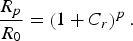 $$\displaystyle{{R_p } \over {R_0 }}=\left( {1+C_r } \right)^p .$$
This averages radius of the piecewise approximated radial strip is used for the calculation of its characteristic impedance as described next.
Due to symmetric or even mode excitation, the electromagnetic interaction in the radial combiners is predominantly due to radial waves in dominant mode, axially symmetric with respect to the feed line which only excite TEM mode. This even mode description is valid as combiner is used normally in electrically symmetric configuration with equal potential on all branch ports. In practice, propagation of higher-order modes is easily prevented by careful design and good mechanical symmetry. As stated earlier the dominant mode description for a circular RTL resembles the TEM mode. In fact, the electromagnetic field configuration for the segmented radial line is nearly identical to that of an ideal strip line, having planar inner conductor in the middle and ground planes on its top as well as bottom, duly separated by a dielectric material having adopted here, the segmentation mechanism is used for the calculation of ∈r. The radial line in the proposed combiner is strip line type (or slab line). Hence, suitable changes in calculation, for taking into account the finite thickness t of the strip/slab, is needed. The characteristic impedance for the slab-type radial line, at the radius r, becomes [Reference Jain, Sharma, Gupta and Hannurkar44]
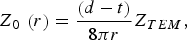 $$Z_{0{\rm \; }} \left( r \right)=\displaystyle{{\left( {d - t} \right)} \over {8{\rm \pi }r}}Z_{TEM},$$
Here r is the radius of the slab-type radial line. Also d and t are defined in accordance with Fig. 1 and Z TEM is given as
 $$Z_{TEM}={\rm \; }\displaystyle{{120{\rm \pi }} \over {\sqrt {{\rm \epsilon }_{\rm r} } }}.$$
Although, this formula was derived by neglecting presence of fringing capacitance, it gives approximate real value to probe ahead. By substituting the value of average radius from (5) in (7) in place of r, the characteristic impedance of the successive strips can be calculated.
In summary, the radial waveguide is modeled by a cascade of transmission lines with the characteristic impedances and physical lengths, described by the geometric progressions. This completes the calculation for the relative input impedance of the radial line. Using this analysis, the value of the input impedance Z c (Fig. 2) at radius r a, contributed by the annular ring of length (r b−r a), can also be computed with the radial line theory described above, by treating the open circuit at one end. The calculation of r c depends more on the electric field, which can be sustained in the annular region having width of (r c−r b) and also on the footprint of N connectors to be placed along the periphery of the radial line. This placement must provide some space for the cable movement, while making a connection. Hence, a few iterations may be required before the final selection. As the outcome of this calculation process, values of radii r a, r b and r c can be calculated. Having analyzed the combining path, the next step in this procedure is the design of the feed line.
B) Designing feed line
The feed line consists of cascaded sections of CTL with stepped inner conductor (Fig. 1) to match the radial line impedance to the 50 Ω impedance at the main port. The radius of the outer conductor of these line sections is kept equal. Thus, the length and the radius of inner as well as outer conductors, for each line section, are used as the design parameters for impedance matching [Reference Abrie45] in the circuit model optimization. The fringing effect caused by the abrupt step discontinuity of inner conductor is modeled by a small static capacitance C j, [Reference Somlo46] given by
 $$\eqalign{C_j&=\displaystyle{{{\rm \varepsilon }_0 } \over {100\pi }}\left[ {\displaystyle{{\tau _1^2+1} \over {\tau _1 }}\ln \left( {\displaystyle{{1+\tau _1 } \over {1 - \tau _1 }}} \right) - 2\ln \left( {\displaystyle{{4\tau _1 } \over {1 - \tau _1^2 }}} \right)} \right] \cr & \quad +\displaystyle{{1.11} \over {1000}}\left( {1 - \tau _1 } \right)\left( {\tau _2 - 1} \right)\left( {{\rm pF}/{\rm cm}} \right),}$$
where
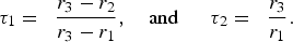 $$\tau _1={\rm \; \; }\displaystyle{{r_3 - r_2 } \over {r_3 - r_1 }},\quad {\rm and\; }\quad \; \tau _2={\rm \; \; }\displaystyle{{r_3 } \over {r_1 }}.$$
Here r 3 is the radius of the outer conductor of a coaxial line having step discontinuity. Also r 2 and r 1 are the radii of the larger and smaller inner conductors, respectively. The capacitance is obtained by multiplying this equation by the circumference (2πr 3) of the outer conductor. For the present design, there are two coaxial steps in the feed line. Hence, the calculation needs to be performed twice by substituting the set of (r 1, r 2, r 3) in (9) with (a 1, a 1, b) and (a 2, a 3, b), with reference to Fig. 1. This step completes the first-order design of the feed line.
In order to account for the effect of the discontinuity at the coaxial/radial line junction (modeled by sub-circuit RTL junction in Fig. 2) additional reactive components, contributing to the input impedance of the coaxial and radial lines, need to be estimated. Williamson [Reference Williamson47], modeled this junction in terms of reactive components viz. B 1, B 2 and B 3, as shown in Fig. 4.
Fig. 4. Equivalent circuit of radial-line/coaxial-line junction.
Using this model and the expressions given in [Reference Fathy, Lee and Kalokitis31], the impedance at the coaxial port of the junction can be derived as
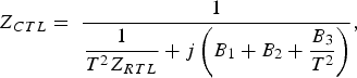 $$Z_{CTL}={\rm \; }\displaystyle{1 \over {\displaystyle{1 \over {T^2 Z_{RTL} }}+j\left( {B_1+B_2+\displaystyle{{B_3 } \over {T^2 }}} \right)}},$$
where Z CTL is the impedance at the coaxial port (measured at M-probe CTL in Fig. 2), Z RTL is the impedance of the radial line and T is the turn ratio of the transformer, as shown in Fig. 4.
C) Full-wave electromagnetic structure simulation
After completing the design of constituting parts of the combiner, it is necessary to simulate its physical structure, for the final optimization, with the help of a 3D full-wave structure simulator. In this simulation, different geometrical parameters of the feed line, radial line, and location of branch port connectors need to be fine-tuned to achieve the desired goal. This goal often involves optimization of important parameters like return loss at the main port, insertion loss of the combiner, and isolation among branch ports. Finally, possibility of the electric field breakdown needs to be studied by providing sufficient spacing between the inner and outer conductors of the different transmission lines and by removing sharp corners of the structure.
III. EXPERIMENTAL INVESTIGATION AND MEASURED RESULTS
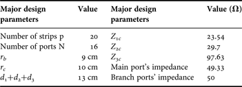
In order to demonstrate theoretical calculation described in the previous sections, a 16-way RF power combiner was designed and fabricated at the center frequency of 505.8 MHz. The design concepts are equally applicable to higher frequency range. The choice of this frequency is useful for the institute's on-going project of the development of a 75 kW solid-state amplifier. The design specifications require the combining efficiency to be better than 95% at the combined power of 16 kW (average). A bandwidth of 40 MHz and a minimum return loss of 15 dB throughout this bandwidth should be achievable. As the output (main) port needs to handle the total power within 16 kW, the standard rigid coaxial line with EIA 3-1/8″ flange, was selected for this port. Similarly for branch ports, expecting the maximum power within 1 kW, standard N-type connectors were selected. The standard Teflon™ material was used as a dielectric to increase breakdown strength as well as to provide a support for the inner conductor of the radial line. The major calculated design parameters are tabulated in Table 1. No any tuning screw or isolation resistors were used in this design. After this initial design calculation, an electromagnetic model was developed for the full-wave simulation using HFSS. During this simulation, the design was fine-tuned to absorb discontinuities at different interfaces and a care was taken to remove any high electric field hot-spots in the constricted regions of the combiner. At such spots, a possibility may exist for the dielectric failure at the full-RF power. The HFSS model of the combiner and its fabricated version are shown in Fig. 5.
Fig. 5. EM model of 16-way high-power RF combiner (left) and its fabricated version.
Table 1. Major design parameters.
For its reliable and round the clock operation, it is necessary to dissipate the heat developed by the RF power loss (incurred inside the combiner) and by the thermal conduction, from coaxial cables connecting at the branch ports. Hence, cooling fins were provided on the outer conductor of the feed line. The simulated value of the maximum electric field, near the branch ports, was 1025 V/m with input power of 1 W at the main port. This result shows an improvement over the value for L-shaped probe, reported in [Reference Li, Liu and Zhang33].
For this combiner, low-power and high-power continuous-wave RF measurements were carried out for validating the design procedure and for demonstrating its suitability at the high power. At the low power, vector measurement in terms of scattering parameters, was carried out using network analyzer E5071B. For the high-power measurement, a solid-state RF amplifier at 20 kW, developed in-house [Reference Jain48], was utilized. In an ideal combiner, the amplitude and phase of the RF signal, fed from the main port, should get distributed uniformly among the branch ports. Thus, the ideal value of transmission coefficient (s oi, i = 1, 2…16), defined as the ratio of forward power wave from the ith port to the output forward power wave at the main port (assigned zeroth port) with all other ports matched terminated, is 12 dB for a 16-way combiner. However, in practice, some imbalances in the amplitude and phase are observed due to an imperfection in the mechanical symmetry of the combiner structure during fabrication. The amplitude and phase of the transmission coefficient s oi, at 505.8 MHz, are shown in Fig. 6. The calculated value (from HFSS) is also shown here. Due to the inherent symmetry of the radial line, used in this combiner, the peak to peak deviations of this coefficient are only 0.18 dB in the amplitude and nearly 2° in the phase. Such negligible imbalance allows a repeatable design with low scattering loss [Reference Gupta6], incurred due to the mismatch/reflection at its various junctions of the solid-state amplifier architecture.
Fig. 6. Transmission coefficient for 16-way combiner at 505.8 MHz.
The return loss and the insertion loss, measured at 1 kW (average) power are shown in Fig. 7. The calculated return loss, shown in the same figure, satisfies 15 dB criteria from 480 to 520 MHz, whereas its measured value is below 15 dB from 483 to 520 MHz. The minima points of the calculated and measured return loss differ by a value of 5 MHz. The insertion loss, shown here, was measured by fabricating two similar 16-way combiners. They were connected back to back so that one combiner performs dividing action, whereas other one combines the divided power. The de-embedded insertion loss for a single combiner was <0.1 dB at 500 MHz. The corresponding combining efficiency [Reference Galani, Lampen and Temple5], is better than 95% from 478 to 520 MHz with a maximum value of 98.7% at 500 MHz. This value reconfirms negligible power lost due to the amplitude/phase imbalance, measured at the low power. Such feature makes this combiner attractive for the high-power solid-state amplifier used in the particle accelerators.
Fig. 7. Return loss and insertion loss of the fabricated 16-way combiner.
A comparison of the calculated and measured isolation among the branch ports, at 505.8 MHz and 16 kW of RF power, is shown in Fig. 8. The minimum value of the isolation (about 10 dB) is exhibited among adjacent branch ports (2 and 16), whereas diametrically opposite ports (8, 9, and 10) are moderately isolated.
Fig. 8. Computed and measured isolation of 16-way combiner at 505.8 MHz.
A cyclic behavior, observed in this isolation pattern, must be due to the existence of higher-order modes in the radial line when it is driven unsymmetrically. For the ideal case of even mode excitation at branch ports, the TEM mode was assumed in radial line, and as can be seen in the simulated E-field pattern of this line, plotted in Fig. 9, this is clearly not the case here. Here branch port 1 is driven port whereas all other ports are matched terminated. It can be deduced that the strongest coupling (poor isolation) from port 1 is to its nearby ports.
Fig. 9. Simulated E-field pattern with port 1 (coinciding with x-axis) as driven port.
For the prolonged time testing, this combiner was tested using an in-house developed solid-state amplifier [Reference Jain48] at 16 kW RF power for more than 7 h. After this test, no any degradation in RF performance was observed. Finally in the series of these experiments, for safety purpose, the radiation level was measured outside the combiner. Its measured value was <0.1 mW/cm2, which is well below the safe limit prescribed in the frequency range of 300–800 MHz. As this combiner is need to be deployed as a workhorse in the on-going solid-state amplifiers, its performance repeatability was checked by fabricating more than 20 such combiners. All these units were rigorously tested at full power without any degradation or any failure.
IV. CONCLUSION
The theoretical design and experimental work on a high-power multi-way radial combiner, required for the solid-state amplifiers, utilizing the cutting edge technology of solid-state devices, is presented here. This design makes use of a rigid mechanical structure comprising a parallel slab (stripline-type) radial line and a coaxial transmission line. A simplified calculation of the radial line impedance using the segmentation approach is performed, followed by its full-wave electromagnetic simulation. Based on this methodology a 16-way power combiner, capable of handling 16 kW of power at 505.8 MHz, was developed and experimentally demonstrated. Its measured results, elongated time testing and repeatability of RF performance, for 20 such combiners, pave the way toward its implementation as a workhorse for the divide and combine strategy adopted in the solid-state RF amplifiers. The absence of any external tuning mechanism and the isolation resistor make this design efficient, repeatable, economic, reliable, and mechanical-friendly.
ACKNOWLEDGEMENTS
We are grateful to Dr. P. D. Gupta for his constant encouragement for this work. We are grateful to Mr. V. Bhalla, Mrs. V. Sekar, and Mr. D. K. Verma for assisting in assembly and RF testing work.
 Akhilesh Jain received M. Tech. in Electromagnetics (Microwave Engineering) from Indian Institute of Technology, Kanpur in 1994. He joined Raja Ramanna Centre for Advanced Technology (RRCAT), Indore in 1994. Since then, he is engaged in the research and development of high-power solid-state radio frequency and microwave amplifier and related components. His main areas of interest are harmonic tuned solid-state power amplifiers, radial power combiners, dielectric resonator loaded structures, and system level analysis for high-power amplifiers.
 Alok Gupta completed his M. Tech. from Department of Electrical Engineering, Indian Institute of Technology, Kanpur in 2005. Since then, he is posted as scientific officer at RRCAT. His main areas of interest are radio frequency amplifier, power combiners, directional couplers, and similar high-power rigid line components.
 Deepak Kumar Sharma completed his Bachelor of Engineering degree from Rajiv Gandhi Technical University. He joined orientation course on advanced technologies under Department of Atomic Energy and was appointed as a scientific officer in RRCAT. Since then he is working in the field of high-power solid-state radio frequency amplifiers for various particle accelerator applications.
 P.R. Hannurkar received his Bachelor of Engineering degree in Electronics and Telecommunication from University of Pune. He served as a Scientific Officer at Bhabha Atomic Research Centre (BARC) Mumbai, after graduating from 20th batch of BARC Training School at Mumbai. In 1986, he moved to RRCAT, Indore and steered the development activities for radio frequency and microwave systems for various particle accelerators, being built at the center. Presently he is leading research and development activities in the front line areas of high-power radio frequency and microwave sources, and particle accelerators for various applications.
 Dr. S.K. Pathak did Ph.D. in Electronics and Communication Engineering from the Department of Electronics and Communication Engineering, IIT, BHU, Varanasi. His research interest includes applied electromagnetics, bio electromagnetics, microwave scattering and antennas, microwave engineering, etc. He has one US patent and has published more than 26 papers in reputed journals.