I. INTRODUCTION
The need for wideband high average efficiency and highly linear power amplifiers (PAs) has increased recently to fulfill the requirements of the base stations in modern third generation (3G) and fourth generation (4G) communications systems. Recently, research works have been conducted on extending the bandwidth capability of the Doherty amplifier [Reference Doherty1–Reference Raab4]. However, a number of bandwidth limiting factors makes it difficult to maintain wideband performance in the Doherty amplifier. Among others, the frequency-sensitive output combining network, input and output offset lines, as well as the frequency-dependent input impedance of the peaking device are dominant factors which limit the bandwidth capability of this amplifier architecture. Nevertheless, solutions have been recently proposed to extend the bandwidth of the Doherty amplifier [Reference Bathich, Markos and Boeck5–Reference Qureshi, Li, Neo, van Rijs, Blednov and de Vreede14]. Low-Q output combining network was implemented in [Reference Bathich, Markos and Boeck5] to extend the bandwidth up to 42%. In [Reference Sun and Jansen6, Reference Bathich and Boeck7], a technique was used to absorb the impedance degradation effect of the output combining network, resulting in high and more flat back-off performances over the targeted design bandwidths. Implementation of suitable broadband input and output matching techniques were also proposed in [Reference Kang, Kim, Moon and Kim8] to achieve wideband Doherty behavior. A modified output combining network using specific characteristic impedance for the impedance inverter and a Klopfenstein output transformer was proposed in [Reference Wu and Boumiza9] to extend the bandwidth of the Doherty amplifier.
However, most published wideband Doherty amplifiers considered amplifier operation up to 6 dB back-off level, which results in low average efficiency for signals with peak-to-average-power ratios (PAPR) of higher than 6 dB.
In this paper, a wideband asymmetrical Doherty amplifier will be designed and implemented over 1.7–2.25 GHz. This design band is rich of wireless communications standards such as UMTS and LTE [15]. The amplifier is intended to provide high efficiency at 9 dB back-off operation over the targeted design band. A number of performance enhancement techniques will be applied with the goal to obtain high and flat back-off efficiency over the targeted band.
The paper first discusses the most important factors that affect the bandwidth capability of the Doherty amplifier (Section II). In Section III, an analysis of the bandwidth capability of the output combining network of asymmetrical Doherty amplifier will be derived and discussed. The derived expressions represent a generalized analysis of the output combining network that applies not only for 6 dB back-off operation as in [Reference Bathich, Markos and Boeck5] but also for any arbitrary back-off level configuration. Moreover, a compensation technique will be applied to absorb the effect of the output combining network over the targeted design band. Next, design and implementation of the asymmetrical Doherty amplifier for 9 dB back-off operation will be given in Section IV. Final results and conclusions will be summarized in Section V.
II. BANDWIDTH-LIMITING FACTORS IN THE DOHERTY AMPLIFIER
The conventional source of limited bandwidth of the Doherty amplifier is the impedance inverter that interconnects the main and peaking amplifiers. However, other factors to be discussed in this section can also critically limit the bandwidth of the Doherty amplifier and have to be considered as important as the impedance inverter itself. Section III provides an analysis of the output combining network in a Doherty amplifier with arbitrary breaking point configuration. However, in practical implementation of this amplifier architecture, other factors play a significant role in limiting the maximum bandwidth that can be achieved.
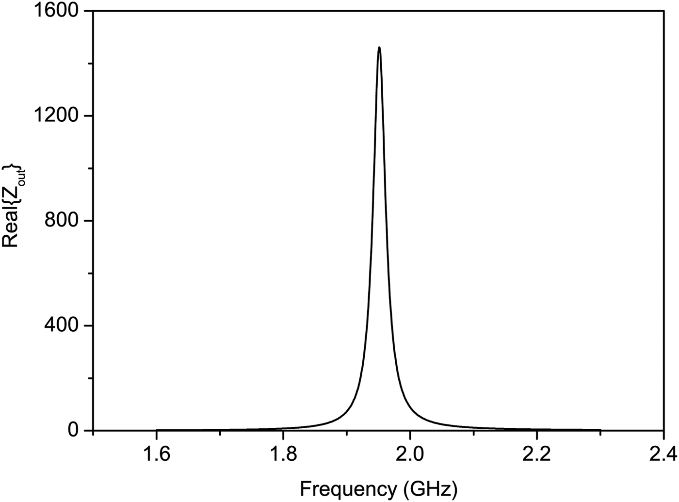
The peaking output offset line is usually used to transform the output impedance seen looking into the peaking amplifier in its OFF state (low-power region) into high impedance magnitude, which minimizes the power leakage from the main amplifier into the peaking amplifier. However, as the operating frequency increases or decreases relative to the center frequency, the output impedance of the peaking amplifier decreases, causing power leakage into this amplifier. The back-off efficiency then degrades as a function of frequency deviation from the design center frequency. As an example, a 10-W GaN HEMT PA was designed to operate in class C mode over 1.6–2.3 GHz. The class C PA was matched to 50 Ω over the design band and an additional output offset line was used. As can be observed from Fig. 1, the output impedance of the PA in its OFF state is highly frequency sensitive and has high magnitude only over a narrow frequency range.

Fig. 1. Real part of the output impedance of a 10-W wideband class C GaN PA (device: CGH40010F from Cree Inc.) with an output offset line in its OFF state.
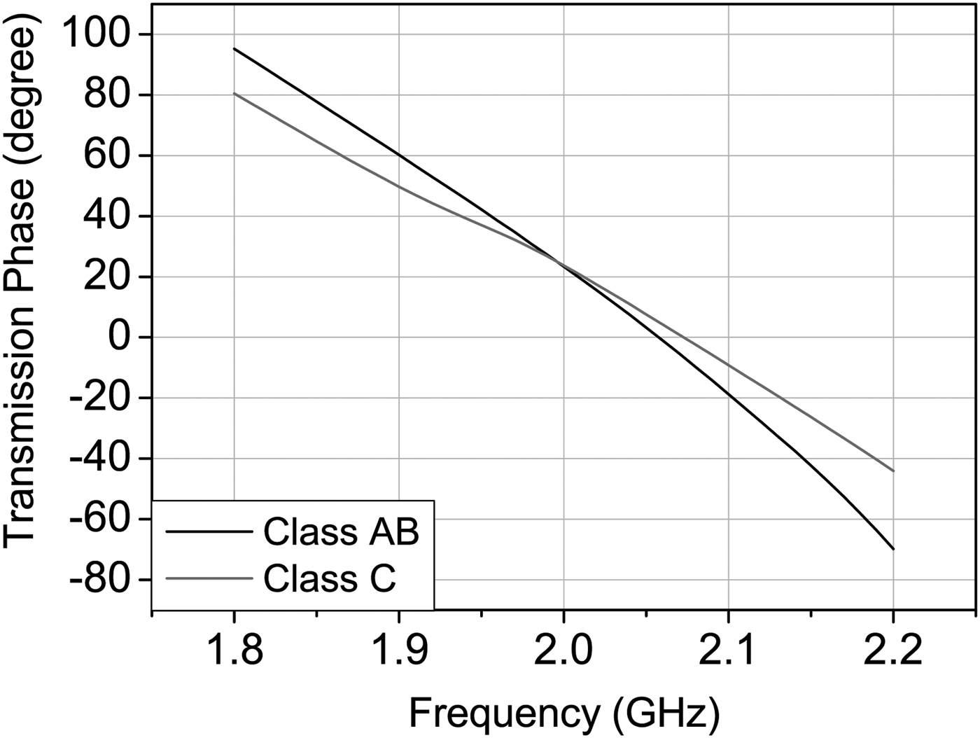
The offset line at the input of the peaking amplifier is also a frequency-sensitive component. This line is needed during operation beyond the breaking point to achieve in-phase combining of the output fundamental currents of the main and peaking amplifiers. In practical implementation of wideband Doherty amplifiers, the phase behaviors of the main and peaking amplifiers might not be similar over the design band due to their different bias and matching conditions, which makes the phase compensation difficult to achieve at all design frequencies using a fixed-length offset line as shown in Fig. 2. A possible solution to this problem could be achieved by optimizing the paths of the main and peaking amplifiers during the design procedure in such a way to make it easier to compensate the phase difference using a fixed-length offset line, e.g. similar input/output-matching network topologies can be used for the main and peaking amplifiers. An alternative solution is to independently inject input power into the main and peaking amplifiers, so that the phase of the input signal can be adjusted for each amplifier at each frequency. However, this solution significantly increases the circuit complexity of the wideband Doherty amplifier and makes further linearization more complicated to achieve [Reference Darraji, Ghannouchi and Hammi16].
Fig. 2. Transmission phase responses of wideband 10 W GaN PAs (1.8–2.2 GHz) biased in class AB and class C modes (device: CGH40010F from Cree Inc.), with the phase difference fully compensated only at 2.0 GHz using a fixed-length offset line at the input of the class C PA.
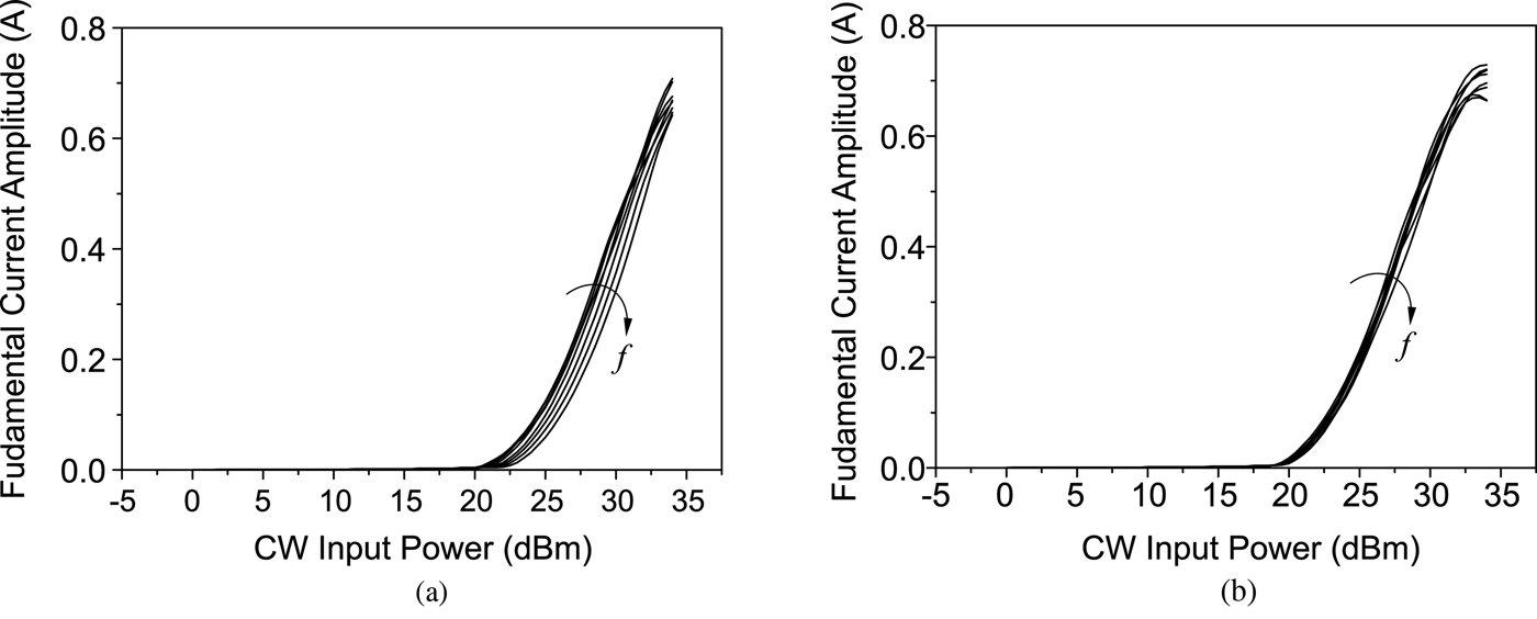
The frequency-dependent turn ON of the peaking amplifier is another factor that affects the wideband capability of the Doherty amplifier. Different gain expansion behaviors of the class C amplifier are obtained at different frequencies, i.e. the drive power level at which the peaking device turns ON is frequency dependent, which affects the load modulation mechanism and results in lower back-off efficiency. Such problem can be solved by careful design of the input-matching network of the peaking amplifier over the targeted design band to make the amplifier turn ON at the same drive power level for all design frequencies [Reference Kang, Kim, Cho, Park, Kim and Kim17] as illustrated in Fig. 3.
Fig. 3. Simulated fundamental output current characteristics of a wideband class C 10 W GaN PA (device: CGH40010F from Cree Inc., frequency range: 1.6–2.3 GHz) (a) by direct injection of drive power into the active device and (b) using wideband input-matching network properly designed to unify the turn ON point over the design band.
III. ANALYSIS AND COMPENSATION OF THE OUTPUT COMBINING NETWORK
In an asymmetrical Doherty amplifier, the breaking point is defined at input voltage of less than half of its maximum, i.e. at power back-off level of higher than 6 dB. This can be numerically expressed as [Reference Lee, Kim, Kim, Cho and Stapleton18]
 $$\sigma=10^{{{ - B} \over {20}}}\comma$$
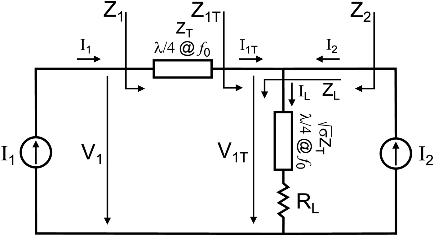
where σ is the normalized input voltage and B is the power back-off level in decibels. For example, σ = 0.5 corresponds to B = 6 dB power back-off. In order for the main device to saturate at a voltage back-off level given by σ, its current source has to see a load impedance of R opt/σ, where R opt is the optimum loadline impedance for maximum power operation. This can be achieved by reducing the common load impedance into a value of σR opt. Consequently, the characteristic impedance of the quarter-wave (λ/4) line that transforms the common load impedance into the final load has to be adjusted as shown in Fig. 4.
Fig. 4. Equivalent-circuit diagram of the asymmetrical Doherty amplifier for B dB back-off breaking point, with the main and peaking devices represented by the current sources (I 1) and (I 2), respectively.
In an asymmetrical Doherty amplifier configuration, the peaking device produces more radio frequency (RF) current than the main device at the maximum power point. The relation between the maximum current amplitudes is given by Lee et al. [Reference Lee, Kim, Kim, Cho and Stapleton18]
 $$I_{2\comma max}=\left({\displaystyle{1 \over \sigma } - 1} \right)I_{1\comma max}\comma$$
where I 1, I 2 are the RF current amplitudes of the main and peaking devices, respectively, as shown in Fig. 4. To achieve asymmetrical current amplitudes, different device sizes should be used for the main and peaking amplifiers. Alternatively, similar devices with different drain supply voltages can be used to control the maximum current swing of each device.
A) Analysis up to the B dB back-off point
Figure 4 shows an equivalent-circuit diagram of the asymmetrical Doherty amplifier, with the main and peaking RF currents represented by the generators I 1 and I 2, respectively. The quarter-wave line with characteristic impedance of Z T interconnects the main and peaking devices to perform the proper load modulation, whereas the other line transforms the common load impedance into the final load impedance of R L.
For the low-power region (up to the B dB back-off breaking point), the peaking device generates no RF current and is assumed to appear as open circuit at any frequency. The RF input voltage at the gate of the main device can be expressed as
 $$V_{in}=AV_{max}\comma \; \, 0 \leq A \leq \sigma .$$
The impedance Z 1T can be written as
 $$Z_{1T}=\sqrt \sigma Z_T \left[{\displaystyle{{R_L+j\sqrt \sigma Z_T \tan \beta l} \over {\sqrt \sigma Z_T+jR_L \tan \beta l}}} \right]\comma$$
which can be used to solve for the impedance Z 1 that is required for the calculation of output power and efficiency [Reference Bathich, Markos and Boeck5].
B) Analysis for the upper B dB regime
In order to solve for the voltage V 1, which enables the solution for output power and efficiency up to the maximum power point, a number of parameters in [Reference Bathich, Markos and Boeck5] have to be redefined to account for the asymmetrical Doherty configuration. The RF main and peaking current amplitudes can be redefined as
 $$I_1=\displaystyle{{I_{max} } \over 2}\left({\lpar 1 - \sigma \rpar \xi+\sigma } \right)$$
and
 $$I_2=e^{ - j\beta l} \displaystyle{{I_{max} } \over 2}\left({\displaystyle{1 \over \sigma } - 1} \right)\xi\comma$$
respectively. For instance, if B = 9 dB, then σ = 0.355 and the ratio I 2,max/I 1,max (at ξ = 1) becomes 1.817. The DC supply power for the main and peaking devices has also to be modified as
 $$P_{DCm}=\displaystyle{{I_{max} \left({\lpar 1 - \sigma \rpar \xi+\sigma } \right)} \over \pi }V_{DC}\comma$$
 $$P_{DCp}=\displaystyle{{I_{max} \left({\displaystyle{1 \over \sigma } - 1} \right)\xi } \over \pi }V_{DC}\comma$$
respectively. The expressions (5)–(8) can then be used to solve for the main device voltage V 1, the main and peaking load impedances Z 1 and Z 2, as well as the output power (P comp) and efficiency (ηcomp) of the asymmetrical Doherty amplifier up to the maximum drive voltage V max [Reference Bathich, Markos and Boeck5]. The derived expressions are still valid for the conventional (B = 6 dB) as well as for any arbitrary asymmetrical Doherty amplifier (B > 6 dB).
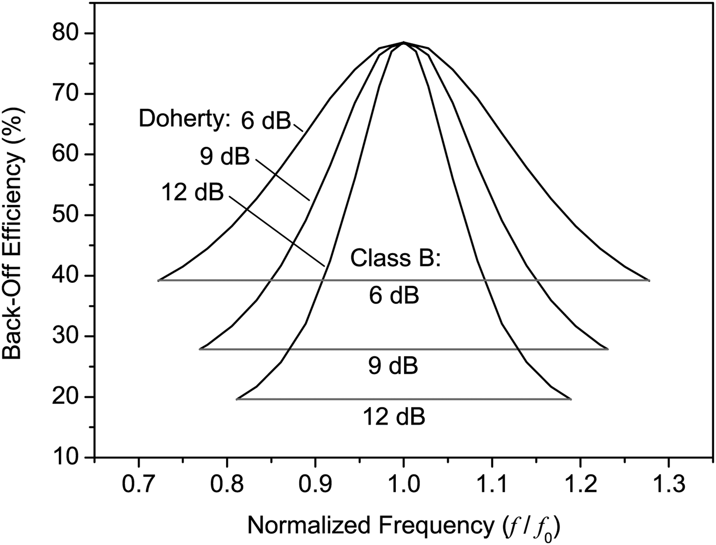
Based on the performed analysis, the back-off efficiency of the Doherty amplifier was calculated for B = 6, 9, and 12 dB as shown in Fig. 5. Although the conventional Doherty amplifier can achieve up to 56% bandwidth, the asymmetrical Doherty amplifier achieves less bandwidth of 46% for 9 dB back-off and 38% for 12 dB back-off configurations. The reason for the narrower bandwidth in the asymmetrical case is the reduced common load impedance of σR opt, which results in increased transformation ratios of the two λ/4-lines comprising the output combining network.
Fig. 5. Calculated back-off efficiency of the asymmetrical Doherty amplifier for various breaking point configurations (B = 6, 9, and 12 dB) versus normalized frequency, with reference to the corresponding back-off efficiency of ideal class B amplifier for each case.
IV. DESIGN OF 80-W WIDEBAND ASYMMETRICAL DOHERTY PA
A wideband asymmetrical Doherty PA was targeted for design to operate within the band 1.7–2.25 GHz with extended back-off performance up to 9 dB. A 35-W GaN HEMT was used as main device (CGH40035F), whereas a 45-W device (CGH40045F) was used as peaking device. Asymmetrical drain supply voltages were applied to the active devices to achieve the required asymmetrical current amplitudes [Reference Kitahara, Yamamoto and Hiura19]. In this regard, a main supply voltage of 20 V was used to reduce the maximum RF current swing of the main device. On the other hand, a peaking device supply voltage of 36 V was used to provide more RF current. The peaking gate bias voltage was chosen to allow turn ON of the peaking device at 9 dB back-off power. Choosing a reduced common load impedance of σR opt = 17.75 Ω, the final λ/4-line had a characteristic impedance of 29.8 Ω instead of the conventional 35.35 Ω.
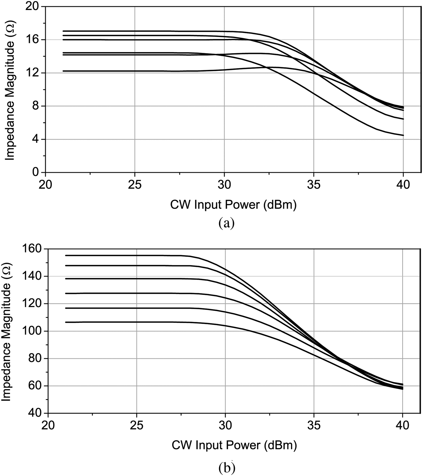
The output-matching network of the main amplifier was designed with the goal to absorb the impedance degradation effect of the output combining network. Figure 6 shows the load impedance modulation behavior at the drain of the main device as well as at the output port of the output matching network, simulated over 2.0–2.25 GHz. At the output of the matching network, the impedance ranged from 106 to 155 Ω in the low-power region, whereas at the drain of the main device, the impedance had a smaller variation from 12 to 17 Ω. The compensated impedance degradation achieved at the device reference plane will result in high back-off efficiency over the design band [Reference Sun and Jansen6, Reference Bathich and Boeck7]. The matching network design also took into consideration the realization of optimum second harmonic load reflection coefficient (obtained from harmonic load-pull simulations) to further increase the back-off efficiency. The wideband asymmetrical Doherty PA was fabricated as shown in Fig. 7.
Fig. 6. Simulated load impedance modulation of the main PA over 2.0–2.25 GHz (a) at the drain of the active device and (b) at the output port of the output-matching network.
Fig. 7. Photo of the wideband asymmetrical Doherty PA prototype.
CW large-signal measurements were performed. Figure 8 shows the simulated and measured efficiency of the Doherty PA at 1.8 GHz for various main device supply voltages. As can be observed, more extended power range could be obtained at smaller drain voltages due to the increased asymmetry between the main and peaking RF currents. Good agreement between simulated and measured data can be also observed from the figure.
Fig. 8. Efficiency of the asymmetrical Doherty PA at 1.8 GHz, simulated (solid lines) and measured (lines with symbols) at main device supply voltages of 16, 20, and 24 V.
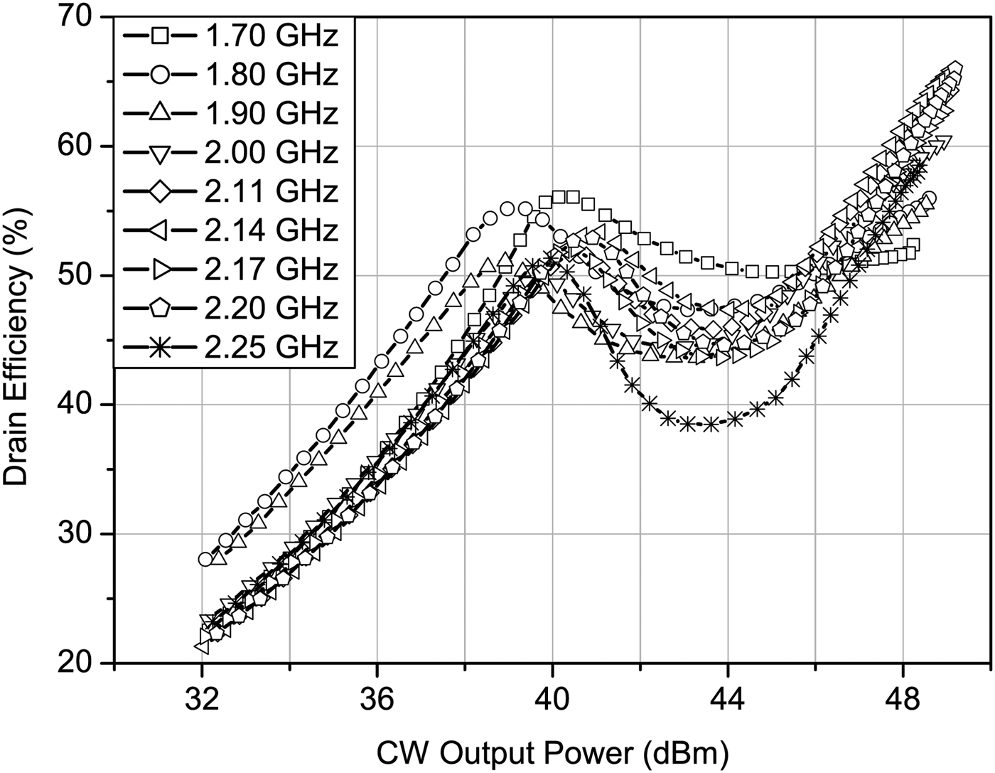
CW measurements were performed over 1.6–2.3 GHz. The maximum output power ranged from 48.2 to 49.1 dBm. It can be observed that the efficiency first peaks occurred near 40 dBm of output power, which is higher than 6 dB back-off power as shown in Fig. 9. High and relatively flat back-off efficiency was measured over the design band as depicted in Fig. 10. The back-off efficiency ranged from η = 50% [power-added efficiency (PAE) = 45%] at 2.0 GHz to η = 57% (PAE = 53%) at 1.75 GHz, which represented a back-off level of 8.0–9.9 dB from the maximum measured output power over the design band.
Fig. 9. Measured efficiency versus CW output power of the asymmetrical Doherty PA over 1.7–2.25 GHz.
Fig. 10. Measured CW output power and efficiency of the wideband asymmetrical Doherty PA at power saturation as well as at 8.0–9.9 dB back-off (BOP) operations, over 1.6–2.3 GHz.
The linearity of the asymmetrical Doherty PA was characterized at the UMTS center frequency of 2.14 GHz. A single-carrier W-CDMA signal (PAPR = 8.0 dB) was used for ACLR characterization. Figure 11 shows the measured ACLR levels and the corresponding average efficiency. At average output power of 40.9 dBm, efficiency of η = 46% together with ACLR = −32 dBc were observed. Using memory polynomial DPD linearization, the linearity was enhanced to ACLR = −43 dBc without influencing the average efficiency.
Fig. 11. Measured average drain efficiency and ACLR levels (+5 MHz offset) of the asymmetrical Doherty PA, before and after DPD linearization, using a 5-MHz single-carrier W-CDMA downlink signal with PAPR = 8.0 dB at 2.14 GHz.
V. CONCLUSION
In this paper, wideband 80 W asymmetrical GaN Doherty amplifier was designed and implemented to cover 28% bandwidth extending over 1.7–2.25 GHz. A number of design improvement techniques were followed to enhance the wideband back-off performance. A generalized frequency response analysis was also performed, which can be applied to the conventional as well as the asymmetrical Doherty amplifier configurations with arbitrary breaking point. The designed Doherty amplifier had superior performance over the design band, where efficiency of higher than η = 50% (PAE = 45%) was maintained at 8.0–9.9 dB output back-off, over the design band. The amplifier linearity was measured using a W-CDMA signal. At average output power of 40.9 dBm and average efficiency of η = 46%, ACLR was enhanced using DPD pre-distortion to −43 dBc. To the best of authors' knowledge, the presented PA in this paper is the first wideband asymmetrical Doherty PA reported so far with high back-off efficiency over such bandwidth.
ACKNOWLEDGEMENT
The authors would like to acknowledge Cree Inc. for providing the large-signal models of the GaN HEMTs used in this work.
Khaled Bathich (M'08) was born in Aleppo, Syria, in 1983. He received his B.Sc. degree in Electrical and Computer Engineering from the Hashemite University, Jordan, in 2005. He obtained his M.Sc. and Ph.D. degrees in Electrical Engineering/Microwave Engineering from the University of Kassel, Germany, in 2007 and Berlin Institute of Technology, Germany, in 2013, respectively. He is currently a microwave design engineer at Novero Automotive in Brandenburg, Germany. His research interests include efficiency-enhancement power amplifier techniques, particularly the Doherty technique.
Georg Boeck (M'93–SM'00–F'08) received the doctoral degree from Berlin University of Technology, Berlin, Germany, in 1984. In the same year, he joined Siemens Research Laboratories in Munich, Germany, where his research areas were on fiber optics and GaAs electronics. Since 1991, he has been the head of the Microwave Engineering Research Laboratory at Berlin University of Technology. Since 2008, he has been with the Ferdinand-Braun-Institut (FBH) in Berlin, Germany, where he is head of the business area microwave power modules. In 2009, he was a co-founder of GloMic GmbH. His main areas of research are power amplifiers, microwave devices, circuits, and systems up to and beyond the 100 GHz range. Professor Boeck has authored or co-authored more than 270 technical papers and one book. He served as IEEE distinguished microwave Lecturer during the years 2006–2008, as an associate editor of the Journal “IEEE Microwave and Wireless Components Letters” in 2008 and 2009 and as a guest editor of the “IEEE Journal of Solid State Circuits” in 2012. He is a member of several Technical Program Committees, a member of the editorial board of the Journal “Frequenz” and a steering committee member of the IEEE Radio Frequency Integrated Circuit Symposium. He was the Chairman of the IEEE Conferences “GeMIC 2010” and “PRIME 2010”. Professor Boeck is a member of the Informationstechnische Gesellschaft (ITG) in the Verband Deutscher Elektrotechniker (VDE), Germany, the Chairman of the German IEEE MTT/AP joint chapter since 2010 and a member of the IEEE SSCS, MTT, and COM Societies.