I. INTRODUCTION
Federal Communications Commission's (FCC) devotion of frequency band from 3.1 to 10.6 GHz for ultra-wideband (UWB) radio applications has presented a leisure and challenge for antenna designers to develop antennas technology that act in this very wide frequency band. The FCC first approved rules for the lucrative use of UWB in February 2002. The FCC gave logic structure for the unlicensed use of the technology in this UWB [1]. Since then, the possible design and creation of UWB systems has become a highly contestable topic for research and development in academia and telecommunications mystery. The antenna forms an important element of UWB systems and hence has created considerable interest for research in recent years [Reference Ma and Jeng2]. Challenges involved with the expansion of a possible UWB antenna design for consumer electronics applications include impedance match and radiation stability over the entire UWB, and also a small size and low manufacturing cost. Among the planar antennas designs in the recent articles, the slot and different types of antennas are presented in [Reference Ma and Jeng2–Reference Naser-Moghadasi, Sadeghzadeh, Asadpor, Soltani and Virdee6] that are one of the most suitable samples for UWB applications. The important features of slot antennas include wide bandwidth performance, easy manufacture and low cost of manufacturing using conventional printed circuit board (PCB) technology. Is shown that, the field distribution in the slot can be retouched to come off a broad bandwidth with a taper shaped feeding structure [Reference Ma and Jeng2] or with a feeding layout that produce multiple resonances at close bands [Reference Naser-Moghadasi, Asadpor and Virdee3]. Another methods to retouch the antenna's field distribution include using a widened slot (or aperture) or a fork-like stub. Another method in [Reference Naser-Moghadasi, Sadeghzadeh, Asadpor, Soltani and Virdee6] gets an important bandwidth enhancement and assures the UWB bandwidth requirements. Although, the design of using fork-like stub needs a relatively large aperture (21 × 32 mm2) and includes a lot of parameters to optimize the antenna's proficiency. As well as, this antenna cannot be improved easily to achieve a band-notch function, which is a favorable specification for UWB system.
In determining bandwidth of UWB systems there is the band (5.15–5.825 GHz) engaged by wireless local-area networks (WLAN) (IEEE802.11a and HIPERLAN/2). Hence, to eschew interposition with nigh WLAN communication systems, UWB systems require embodying a band-notch or notch filter in their RF front-end. But, this will increase the size and provide dispensable complexity for UWB systems. So, it is therefore favorable to design the UWB antenna with the filtering function formerly made into it in order to minimize/omit interpositions between 5 and 6 GHz [Reference Yoon7]. To design slot antennas with band-notch function, one easy and impressive way is to accommodate slots that demean similar half-wavelength resonant structures aboard the antenna such as U-shaped slot [Reference Su, Wong and Chang8–Reference Choi, Chung and Roh10], V-shaped slot [Reference Kim and Kwon11], a hat-shaped slot [Reference Lee, Park and Choi12], etc. Lately the design of a band-notched UWB slot antenna using square ring resonator has been demonstrated [Reference Lui, Cheng and Zhu13].
In this paper, a new and small micro strip slot antenna with band-rejection function with triple fed and simple structure is presented, that covers the UWB band from 3.1 to 10.6 GHz. The antenna consists of a co-planar wave guide (CPW)-fed rectangular aperture (12.5 × 23 mm2) with a rectangular stub. Further, compared to aforesaid references and [Reference Lin and Hung14], which has a relatively small aperture size of 13 × 23 mm2, the antenna presented in this manuscript has the following advantages:
(1) Significantly reduced dimensions (~35%),
(2) Appropriate gain for UWB application.
The presented is designed and manufactured and the capabilities of the antenna have been validate by test vehicles. It is shown the antenna exposures relatively good performance in terms of impedance match and radiation stability over the entire UWB band, as well as radiating omnidirectionally in the x–z plane (around the y-axis). Furthermore, it is shown that the presented antenna can be easily modified to exhibit non-responsive characteristics at the WLAN interfering frequency band.
II. ANTENNA DESIGN
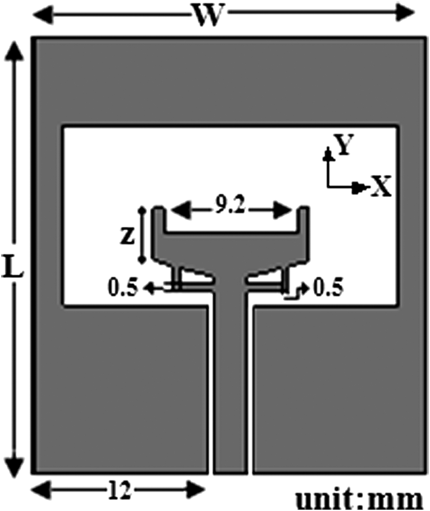
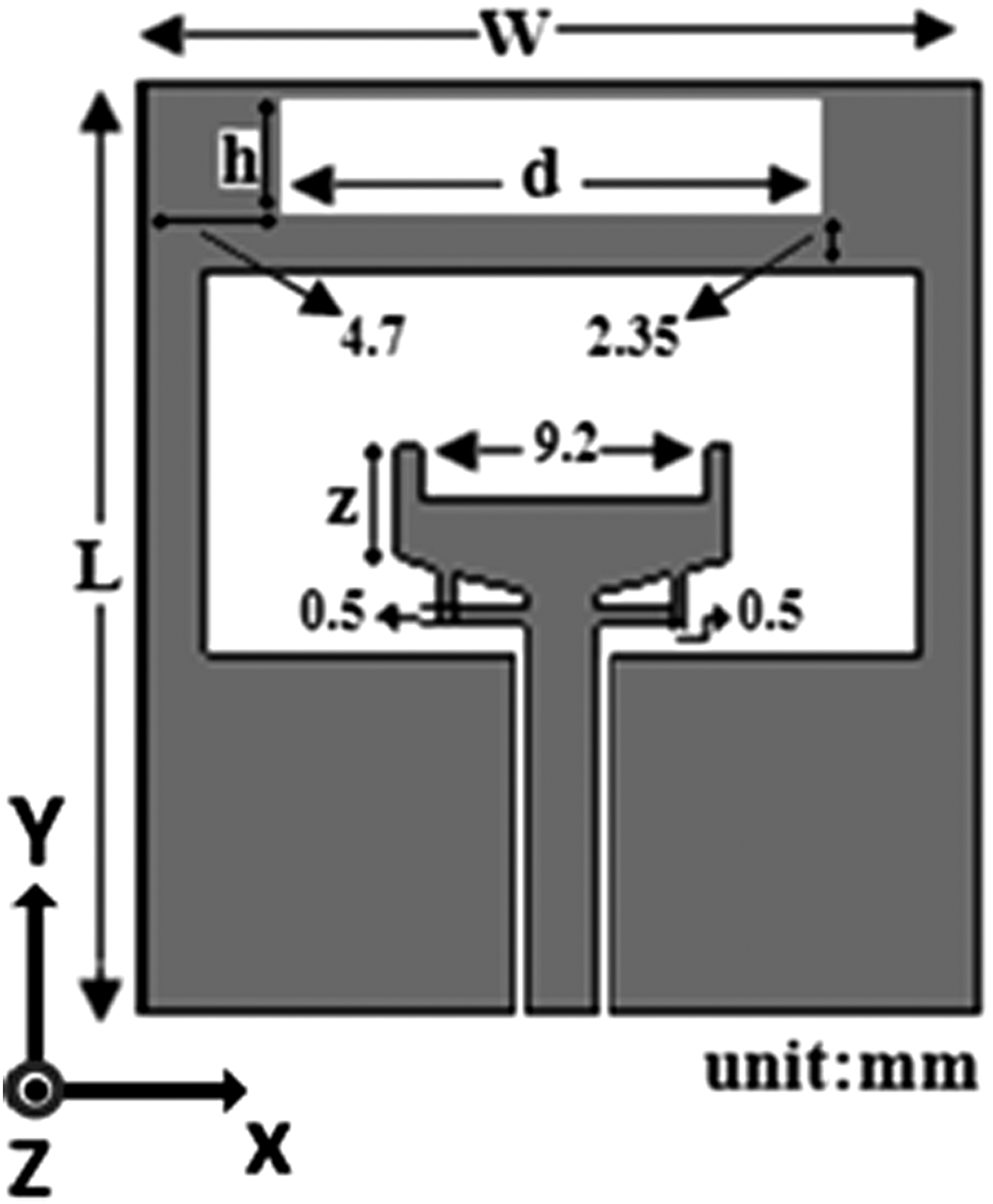
Figure 1 shows the schematic of the presented antenna. The antenna consists of a rectangular aperture created in the ground-plane of a PCB and is excited by a CPW-fed fork-like exciting stub. The fork-like patch is fed by triple-fed structure. This kind of fed prevents the excitation of horizontal currents and ensures that only the dominant vertical current mode is present in the structure [Reference Daviu, Cabedo-Fabres, Ferrando-Bataller and Valero-Nogueira15]. The PCB board is cut in Iran Telecommunication Research Center (ITRC); also the antenna is fabricated and tested in this center. The CPW transmission-line is designed to have a characteristic impedance of 50 Ω. The advantage of this configuration is ease of manufacturing and low cost. The CPW line allows the antenna to be easily integrated with radiofrequency/microwave circuitry on the system board. Reducing the antenna's rectangular aperture area affects its input impedance match over the UWB band, especially at lower frequencies. The aperture area satisfying the antenna's impedance match across the UWB was determined to be 12.5 × 23 mm2. The commercial simulation tool Ansoft HFSS was employed in this paper to analyze and optimize the design [16]. The optimum dimensions of the proposed antenna parameters are shown in Table 1.

Fig. 1. Geometry and configuration of the proposed antenna.
Table 1. Antenna parameters.

III. MEASUREMENT RESULTS AND DISCUSSION
The antenna design was manufactured using a low-cost FR4 dielectric substrate with dielectric constant of 4.4 and a thickness of 1 mm. The measurement of VSWR was carried out with an HP8722-ES network analyzer. Figure 2 shows the measured and simulated VSWR of the antenna. This figure shows very good agreement achieved between simulation and measurement results. The figure also illustrate that the input impedance is well matched as the magnitude of the VSWR is <2 across the entire UWB band (3.1–10.6 GHz).
Fig. 2. Measured and simulated VSWR of the proposed antenna with optimal dimensions.
The normalized measured E & H field radiation patterns in the x–z and y–z-planes are plotted in Figs 3(a)–3(f). The simulated and measured radiation patterns are relatively omnidirectional except at 10 GHz, in the x–z plane (around y axis) but in some frequencies the radiation patterns are not constant for all directions as indicated at various spot frequencies in Fig. 4, i.e. the H-plane at 4, 7 and 10 GHz, are shown in Figs 4(a)–4(c) and the E-plane at 4, 7 and 10 GHz, are shown in Figs 4(d)–4(f), respectively. However, the radiation patterns in the H-plane at 4 GHz and the E-plane at 7 GHz, show nulls at grazing angles which are attributed to two different mechanisms. The first mechanism that causes field cancellation at grazing angles is due to the phase difference between fields on the top and bottom of the ground-plane. The results in Fig. 3 show that this phase difference does not exist in the E-plane at 4 GHz and the H-field at 7 GHz. The second reason these nulls occur is because the slot antenna is covered with a dielectric substrate at one side. This forces the normal component of the electric field at grazing angles to go to zero as described in [Reference Balanis17].
Fig. 3. Normalized radiation patterns : (a) E-plane (yz-plane) at 4 GHz, (b) H-plane (xz-plane) at 4 GHz, (c) E-plane (yz-plane) at 7 GHz, (d) H-plane (xz-plane) at 7 GHz, (e) E-plane (yz-plane) at 10 GHz, (f) H-plane (xz-plane) at 10 GHz.
Fig. 4. Transmitted and received signals for face to face case (a) none filtering frequency antenna (b) filtering frequency antenna and (c) antenna orientation (top view).
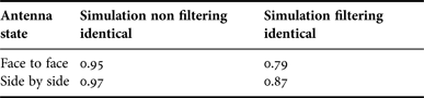
To investigate the performance of the filtering frequency antenna as a transmitter and a receiver in a UWB system, a pair of the identical antenna has been placed in 75 cm distance from each other (antennas are in the far field of the each other) in two different orientations in the free space as it shown in Fig. 4(c). One of the antenna acts as a transmitter and the other one is a receiver. The fidelity factor for each case has been calculated according to the equation (1), this equation is the well-defined parameter named fidelity [Reference Joardar and Bhattacharya18] is proposed to assess the quality of a received signal waveform regarding to the input signal. In this equation s t(t) is the source pulse and s r(t) is received signal by the virtual probes located in the far field of the antenna. The fidelity (F) is the maximum correlation coefficient of the two signals by varying the time delay τ. Indeed, it reflects the similarity between the source pulse and the received pulse.
The fidelity factor for each case has been calculated and summarized in Table 2. The time domain received and transmitted pulses for front to front case for both none filtering and filtering frequency antennas are simulated by CST software and shown in Fig. 4. Owing to the free space loss the received signal attenuate very much which makes difficult to indicate in the figure. Because of that the amplitude of the received signal has been multiplied by 500. As it shown in Figs 4(a) and 4(b), the received signal by filtering frequency antenna has been dispersed and distorted in comparison with none filtering frequency antenna which confirms the fidelity factor results.
 $$F=\max \left[{\displaystyle{{\vint_{ - \infty }^{+\infty } {s_t \lpar t\rpar s_t \lpar t+\tau \rpar d\tau } } \over {\vint_{ - \infty }^{+\infty } {\left\vert {s_t \lpar t\rpar } \right\vert ^2 dt\vint_{ - \infty }^{+\infty } {\left\vert {s_r \lpar t\rpar } \right\vert ^2 dt} } }}} \right].$$
Table 2. Fidelity factor between transmitted and received signals.

IV. BAND-NOTCH DESIGN
To mitigate the interferences with the IEEE802.11a and HIPERLAN/2 WLAN systems operating in the 5–6 GHz band the need for a notch-band function is highly desirable in the UWB system. This paper describes the design of a band-notch UWB antenna and demonstrates the superior features obtained using the proposed antenna employing fork-liked exciting stub scheme. The concept behind the notch-band or band-rejection function is to make the input impedance of the antenna singular (minimum resistance) at the sub-resonant frequency. This is accomplished using a narrow-band resonant structure that is added to the original wide-band antenna. Figure 5 shows the geometry and dimension of the notching structure employed in this paper. By creating a very simple rectangular slit on upper the ground we create the band-rejection characteristic in this antenna. Also this characteristic is tunable by variation parameter of d, that we show this variation in Fig. 6. Hence, the notching structure perturbs the resonant response of the antenna by acting as a parasitic half-wavelength resonant device that is electrically coupled to the rectangular monopole.
Fig. 5. Geometry of the band-notch structure fabricated on the conductor-backed plane.
Fig. 6. Simulated VSWR characteristic for various length d.
Current distribution of the antenna at three different frequencies (4, 5.5, and 7 GHz) was simulated using HFSS and displayed in Fig. 7. It is apparent that, the current distribution is relatively constant at 4 and 7 GHz. However, high density of surface current around the band-rejection structure is observed on the antenna at 5.5 GHz, which implies that the filtering structure resonates near 5.5 GHz. At the notch frequency, the current flows are more dominant around the parasitic element, and they are oppositely directed between the parasitic element and the radiation patch. The simulation results confirm the desired high attenuation near this frequency is produced.
Fig. 7. Simulated results of the surface current distributions over the proposed antennas at: (a) 4 GHz, (b) 5.5 GHz (notched band), and (c) 7 GHz.
From empirical studies it was found that when the band-notch design is applied to the antenna, there is no retuning work required for the previously determined dimensions of the fork-liked stub and aperture of the antenna. The measured and simulated VSWR performance of the band-notched antenna is shown in Fig. 8. Compared to the original design in Fig 2, the band-notched design successfully blocks out the main part of 5–6 GHz band and still performs very good impedance matching (VSWR < 2) at other frequencies in the UWB band. Figure 8(a) shows the measured peak gain spectrum of the proposed antenna with and without band-notch design. A sharp decrease of antenna gain in the notched frequency band at 5–6 GHz can be observed as is desired. The graph shows that the band-notch antenna's gain is greater than unity at other frequencies in the UWB band. In fact the gain rises above unity for increasing frequency. Figure 8(b) shows the simulated radiation efficiency of the proposed antenna as function of frequency for the original and band-notched designs. As shown, in this figure we saw that the radiation efficiency in notch frequency is so reduced (Fig. 9). Figure 10 presents the photograph of the fabricated prototype antenna and the band-notch structure in the conductor-backed plane.
Fig. 8. Measured and Simulated VSWR as a function of frequency of the proposed antenna with band-notch structure.
Fig. 9. (a) Measured co-polarized gain of the proposed antenna as a function of frequency for the original and band-notched designs.
Fig. 10. Photograph of the fabricated UWB antenna: (a) the proposed antenna, and (b) antenna with band-notched structure.
V. CONCLUSION
This paper described a compact antenna suitable for UWB applications. A UWB planar monopole antenna with variable band-stop characteristic has been presented. Reformed fork-liked patch and its triple CPW-fed are utilized to increase the impedance bandwidth. Band-stop characteristic is achieved by adding a simple rectangular slit on the patch. The performance of the antenna was practically verified to show that, it provides band-rejection at the WLAN interfering band 5–6 GHz, and a broad impedance bandwidth and stable radiation patterns across the UWB frequency range. The antenna's radiation patterns are omnidirectional over operating bands. In addition, the antenna exhibits a relatively good gain performance despite its small dimensions. Experimental results show that the proposed planar CPW-fed slot antenna can be a good candidate for UWB applications.
Mohammad Naser-Moghadasi was born in Saveh, Iran, In 1959. He received the B.Sc. degree in Communication Eng. in 1985 from the Leeds Metropolitan University (formerly Leeds polytechnic), UK. Between 1985 and 1987 he worked as an RF design engineer for the Gigatech company in Newcastle Upon Tyne, UK. From 1987 to 1989, he was awarded a full scholarship by the Leeds educational authority to pursue an M.Phil. Studying in CAD of Microwave circuits. He received his Ph.D. in 1993, from the University of Bradford, UK. He was offered then a two years Post Doc. To pursue research on Microwave cooking of materials at the University of Nottingham, UK. From 1995, Dr. Naser-Moghadasi joined Islamic Azad University, Science Research Branch, Iran, where he currently is an Associate Professor and head of postgraduate studies. His main areas of interest in research are Microstrip antenna, Microwave passive and active circuits, RF MEMS. Dr. Naser-Moghadasi is member of the Institution of Engineering and Technology, MIET and the Institute of Electronics, Information and Communication Engineers (IEICE). He has so far published over 140 papers in different journals and conferences.
Loghman Asadpor was born on August 08, 1984, in Urmia, I.R. Iran, He received his B.S. degree in 2010 from the Department of Electrical Engineering, Science and Research Branch, Islamic Azad university, Tehran-Iran. Currently he is pursuing his Ph.D. degree in Electrical and Communications Engineering. His research has included antenna design, and microwave instrumentation & measurement.