


Introduction
Compact antennas with wideband performance are often required for modern wireless devices. Among all the possible technological solutions, planar printed monopole antennas are largely diffused due to their advantages of being lightweight and low profile, low cost, and easy to be integrated with the device's circuit board [Reference Liu, Wu and Tseng1]. Coplanar waveguide (CPW)-fed monopole antennas, furthermore, offer broader bandwidth (BW), allow the integration with surface-mount devices, and can be used for dual-band operations [Reference Lin and Yu2, Reference Chen and Chen3].
CPW-fed monopoles have been implemented with different shapes yielding different performance in terms of BW: a simple monopole strip on a T-shaped slot with 121% of normalized BW [Reference Jiao, Zhao, Zhang, Yuan and Jiao4], a conventional rectangular shape with normalized BW of about 50% in [Reference Ray and Ranga5] or 70% in [Reference Deng, Xie and Li6], circular or annular ring with multiple BWs in [Reference Goswami and Karia7], a Y-shaped monopole with dual-band performance in [Reference Liu and Hsu8], a pentagonal radiating patch with slots for tri-band operation [Reference Liu, Ku and Yang9], hexagon with small fractal elements [Reference Fallahi and Atlasbaf10], a triangular patch in [Reference Wu11], etc. An external CPW-fed slot which surrounds the central monopole element has been also proposed to yield improved BW capabilities, as in [Reference Chiou, Sze and Wong12–Reference Zhao, Ruan and Qu14].
Although CPW-fed monopole antennas can be designed with very broad BWs as demonstrated above, they are not extremely compact. In fact, the monopole in [Reference Chen and Chen3] has been printed on a substrate of size 0.47λ 0 × 0.4λ 0 (with λ 0 calculated at the center frequency); the reference design of [Reference Deng, Xie and Li6] is of total size 0.48λ 0 × 0.35λ 0; in [Reference Liu, Wu and Tseng1], the antenna occupied area is 0.5λ 0 × 0.5λ 0. Miniaturization of CPW monopole antennas and, in particular, the achievement of a good BW/size trade-off is, for this reason, an objective of research activities in this field.
In this paper, a compact CPW-fed monopole antenna is proposed for Wi-Fi and Wi-MAX applications. It has been implemented on a surface of only 0.35λ 0 × 0.27λ 0. A Y-shaped monopole configuration inside a slotted CPW ground (similar to [Reference Liu, Wu and Tseng1] or [Reference Chiou, Sze and Wong12–Reference Zhao, Ruan and Qu14]) has been chosen for this design. Two equal length arms connected to the basis of the monopole guarantee broadband performance and miniaturized size, with the result of a very high BW/size trade-off. A prototype of final dimensions 28 mm × 36 mm × 1.6 mm is fabricated on a low-cost FR4 substrate, and measurement results show an impedance BW of 46% (10 dB return loss), 2.25–3.6 GHz, and gain larger than 2 dBi. Finally, a metallic reflector of 60 mm × 60 mm is used to enhance antenna gain to 6 dBi without significantly affect the antenna BW performance.
Design of the antenna
The antenna structure is shown in Fig. 1. The proposed antenna is constituted by a CPW transmission line of width w f and symmetric ground gap g printed on the top side of an FR4 substrate (ε r = 4.4 and tan δ = 0.02). The CPW ground plane is extended to occupy the whole surface, whereas a central slot is opened to hold the monopole. The CPW transmission line is connected to a Y-shaped monopole [Reference Liu and Hsu8]. Two equal length arms are connected to the base of the radiation element for impedance matching operation. The CPW dimensions, on the other hand, are taken as optimization parameters for maximizing the BW capability.
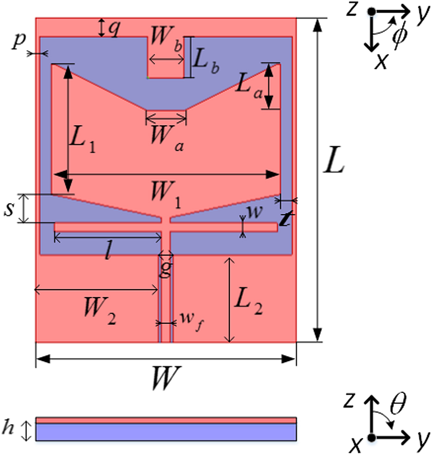
Fig. 1. Structure of the proposed antenna.
An antenna design evolution process is shown in Fig. 2, and S 11 performance curves for each step are reported in Fig. 3.
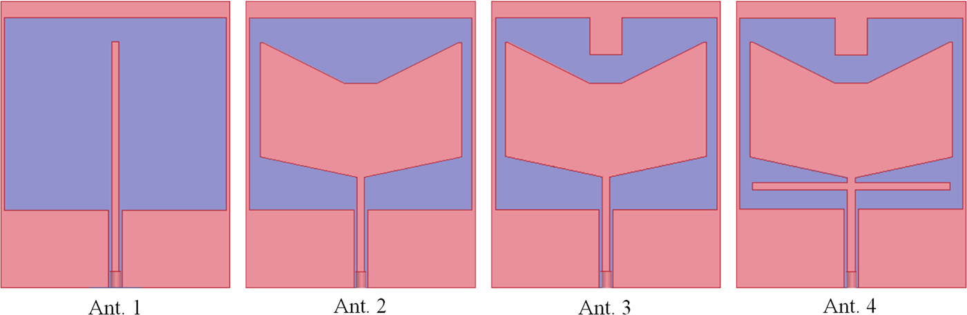
Fig. 2. Antenna design evolution.

Fig. 3. S 11 performance for each step of the design evolution.
As it can be seen, exciting the CPW slot with a simple monopole as in Ant. 1 produces a resonance around the center frequency 2.8 GHz, which is moved down to 2.5 GHz when the straight monopole is substituted with a Y-shaped patch as in Ant. 2. A ground extension which protrudes into the slot as in Ant. 3 improves S 11 performance in terms of both minimum value (from −15.6 dB to about −23 dB) and BW, and increases the current path length of the slot causing another frequency shift toward lower frequencies. Finally, in Ant. 4 two equal length arms are used to match the input impedance of the Y-shaped monopole, and this is demonstrated by Fig. 3 where the second resonance is visible and yields a wideband behavior. From this analysis, it is clear that the first resonance is due to the CPW slot, whereas the second resonance is mainly due to the Y-shaped monopole.
Figures 4(a) and 4(b) depict the surface current distributions at 2.2 and 3.5 GHz, respectively. A significant current distribution is observed on the CPW lateral ground at 2.2 GHz which again proves that the slot is responsible of the first resonance shown in Fig. 3. Similarly, the current is mainly distributed on the two equal length arms at 3.5 GHz, indicating that this part is fundamental for achieving proper matching of the Y-shaped monopole. Meanwhile, a large current on the strip feeder is also present, and it is out of phase with that of the adjacent ground plane. For this reason, the CPW feeder current does not significantly contribute to the radiation in the far-field zone [Reference Liu, Wu and Tseng1].

Fig. 4. Surface currents at different frequencies. (a) 2.2 GHz, (b) 3.5 GHz.
Parametric analysis
A parametric analysis is herein proposed to understand the effect of the different parameters on the antenna performance. Particularly, the effect of the arm length l and width w, the distance between the monopole edge and the side ground plane t, the side and upper ground plane width p and q, and the ground plane parameters W b and L b are investigated in the following.
Effect of arm length l and width w
Simulated antenna performance in terms of S 11 is shown in Fig. 5 as a function of the arm length l and width w.

Fig. 5. Simulated S 11 as a function of (a) arm length l and (b) width w.
The arm length l is shown to be an important parameter to regulate the second resonance frequency, as already described in Section “Design of the antenna”. An increase of l shifts the second resonance toward lower frequencies, with a corresponding reduction of the BW. The increase of arm width w, on the other hand, improves the impedance matching performance at the center of the BW, at the expense of a BW narrowing.
Effect of distance t
The parameter t is directly related to the antenna width W, and it fixes the distance between the monopole and the lateral ground plane. Figure 6 depicts simulated S 11 as a function of t.

Fig. 6. Simulated S 11 as a function of t.
As it can be observed, this parameter has a significant impact on the impedance matching performance of the antenna within the whole BW. In particular, an increase of t with respect to the optimized value improves the impedance matching at the higher frequencies but deteriorates S 11 at lower frequencies, and vice versa for a decrease of t.
Effect of width p and q
The ground widths p and q are also important parameters for the impedance matching and BW regulation. As shown above, the arm length l can be used to move the second resonance frequency; on the other hand, the parameter p regulates the position of the first resonance, as shown in Fig. 7(a), without affects significantly the higher frequency behavior. The parameter q has a similar effect as t for the regulation of the impedance matching performance within the whole BW, as depicted in Fig. 7(b). A trade-off has to be made with these two parameters to optimize both the BW and the impedance matching performance.

Fig. 7. Simulated S 11 as a function of (a) p and (b) q.
Effect of W b and L b
Other two parameters of the ground plane, i.e., W b and L b, are studied, and simulation results are provided in Fig. 8. While W b is important for the optimization of the impedance matching, the parameter L b is used to reduce the antenna's size. In fact, an increase of L b shifts the first resonance toward lower frequencies (see also Fig. 3), and this is due to a longer current path.

Fig. 8. Simulated S 11 as a function of (a) W b and (b) L b.
Measurement results and discussion
The guidelines derived from the parametric analysis proposed above has been used for designing the antenna proposed in this paper. After a final optimization, the antenna parameters are chosen as listed in Table 1. This antenna has been fabricated and a prototype has been used to verify the correctness of the proposed results with a comparison between simulation and measurement. The antenna prototype is shown in Fig. 9.
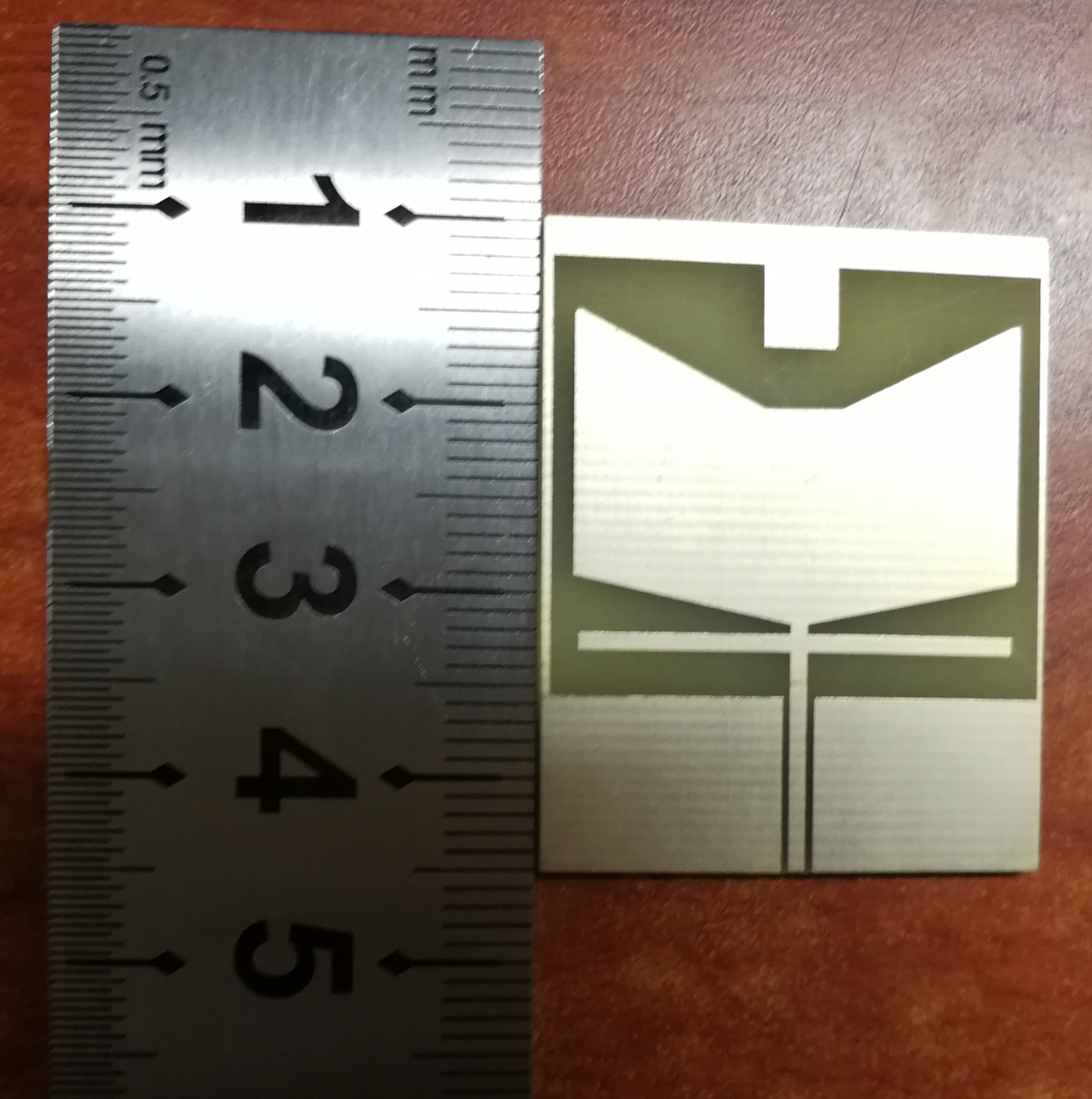
Fig. 9. Fabricated antenna prototype.
Table 1. Antenna dimensions after the final optimization

Bidirectional antenna
Return loss has been measured with the Agilent vector network analyzer (N5230A), and a comparison between simulation and measurement results is depicted in Fig. 10.
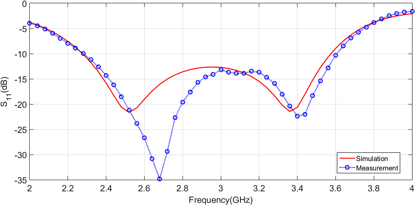
Fig. 10. Simulated and measured S 11 as a function of frequency.
It can be seen that the measurement and simulation results are in good agreement, and this confirms the proposed analysis. Measured impedance BW (defined for S 11 ≤ −10 dB) is from 2.28 to 3.6 GHz (fractional BW of 44.9%).
Radiation patterns and gain have been also measured by using the near-field NSI-800F10 antenna measurement system. Figures 11 and 12 show the measured and simulated antenna gain patterns at 2.5 and 3.5 GHz, respectively, whereas Fig. 13 compares measured and simulated broadside gain as a function of frequency.
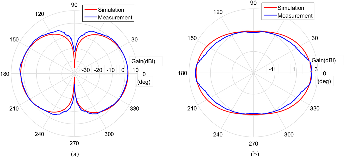
Fig. 11. Simulated and measured gain patterns at 2.5 GHz. (a) E-plane (angles from x to y-axis), (b) H-plane (angles from z to y-axis).

Fig. 12. Simulated and measured gain patterns at 3.5 GHz. (a) E-plane (angles from x to y-axis), (b) H-plane (angles from z to y-axis).

Fig. 13. Simulated and measured broadside gain as a function of frequency.
Unidirectional antenna
In case of point-to-point communication systems, or however in all applications which require longer communication range, a metallic reflector can be placed beneath the proposed antenna to achieve a directive pattern. A foam spacer is used to separate the antenna from a 60 mm × 60 mm copper adhesive surface, as shown in Fig. 14.

Fig. 14. Prototype of the directive antenna.
In Fig. 15, measured (and simulated) S 11 as a function of the spacer height are depicted. As it can be seen, the presence of the metallic reflector deteriorates S 11 performance, and this effect is more visible with the decrease of the spacer height (due to an increase of the destructive contribution between direct and reflected waves within the BW of interest). A spacer height of 30 mm is found to be the minimum value for achieving the wideband behavior, with an S 11≤ −10 dB BW of 1.44 GHz (from 2.16 to 3.59 GHz). Simulation results globally confirm this behavior, even if discrepancies can be found due to fabrication imperfections.

Fig. 15. Measured S 11 as a function of the foam spacer height.
Simulated and measured results of radiation patterns at 2.5 and 3.3 GHz, and broadside gain are also provided in Figs 16–18, respectively.
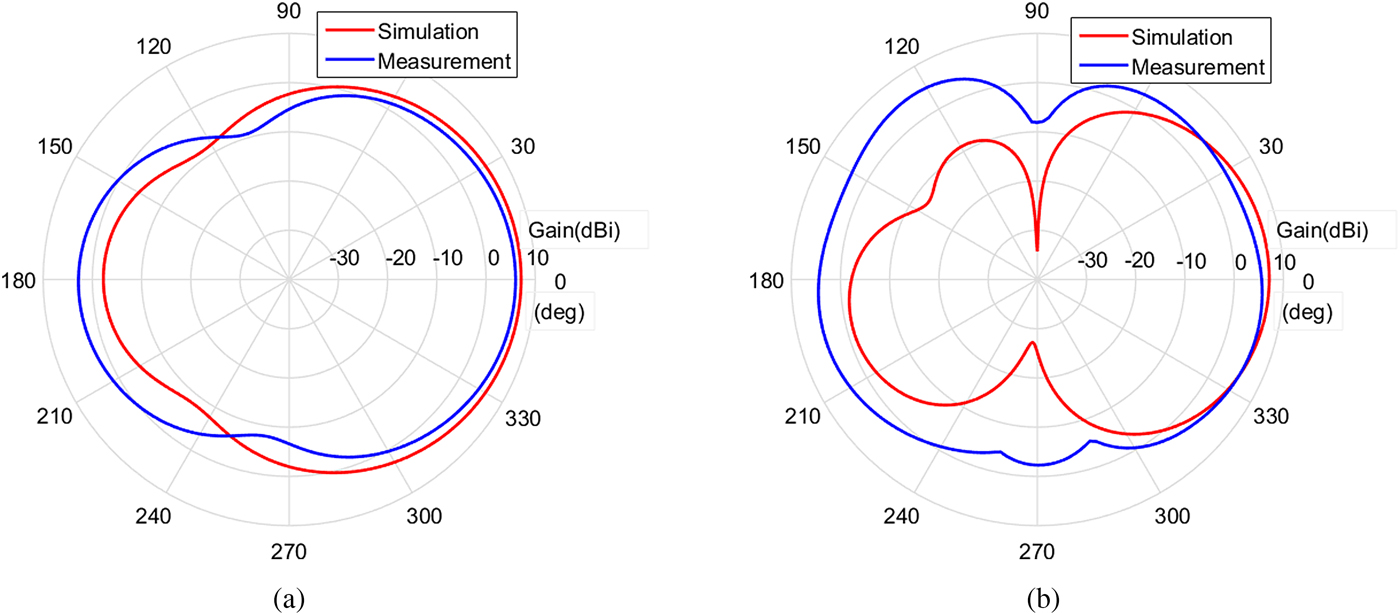
Fig. 16. Simulated and measured gain patterns for the directive antenna at 2.5 GHz. (a) E-plane (angles from x to y-axis), (b) H-plane (angles from z to y-axis).
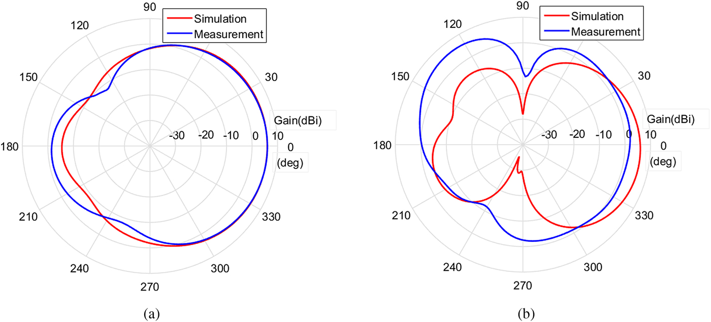
Fig. 17. Simulated and measured gain patterns for the directive antenna at 3.3 GHz. (a) E-plane (angles from x to y-axis), (b) H-plane (angles from z to y-axis).

Fig. 18. Simulated and measured broadside gain as a function of frequency for the directive antenna.
These results clearly highlight that a directive pattern is achieved, with a gain of about 6 dBi toward broadside, at the expense of an increased antenna volume. Furthermore, it should be noted that the selected reflector size only partially limits the back radiation (for both E- and H-planes) as shown in Figs 16 and 17. Front-to-back ratio performance can be improved with an increased reflector size.
Comparison with other antennas
In Table 2, a comparison of the proposed antenna with other CPW-fed slot antennas presented in the technical literature is provided. In order to make a fair comparison, only wideband CPW-fed slot antennas have been considered (and not multiple BW antennas). Particularly, the last column of Table 2 presents a comparison metric which evaluates the trade-off between achieved fractional BW and antenna size.
Table 2. CPW-fed slot antennas comparison

As it can be observed, many wideband CPW-fed slot antennas have been proposed to cover extremely broad BWs. Nonetheless, occupied areas are usually larger than  $0.2\lambda _0^2 $, with only a few exceptions, leading to a BW/size factor lower than 3 (in [Reference Goswami and Karia7], the antenna surface is lower than
  $0.2\lambda _0^2 $ and BW/size is 3.36). The proposed antenna presents the smallest occupied area (<
 $0.1\lambda _0^2 $), with fractional BW of 46% sufficient to deal with Wi-Fi and Wi-MAX applications, with the largest BW/size factor, i.e., 4.84, with respect to the antennas in Table 2. Furthermore, the measured gain is the same as the antenna in [Reference Goswami and Karia7] but employing about half the area.
Conclusion
A compact CPW-fed monopole antenna of size 0.35λ 0 × 0.27λ 0 is proposed in this work. A Y-shaped monopole with two equal length arms configuration is used to both guarantee broadband performance and miniaturized dimensions. A prototype of 28 mm × 36 mm × 1.6 mm has been fabricated on an FR4 substrate for Wi-Fi and Wi-MAX applications, and measurement results have demonstrated an impedance BW of 46% (10 dB return loss), from 2.25 to 3.6 GHz, and gain larger than 2 dBi. The proposed antenna exhibits an outstanding BW/size trade-off better than many other CPW-fed antennas in the literature and, as demonstrated, can also be used to achieve directive radiation pattern (measured gain of 6 dBi) by employing a 60 mm × 60 mm metallic reflector without affecting significantly the antenna BW performance.
Acknowledgement
Authors acknowledge that this work was supported in part by the National Natural Science Foundation of China under project contracts No. 61601093, 61791082, 61701116, and 61371047, in part by Sichuan Provincial Science and Technology Planning Program of China under project contracts No. 2016GZ0061 and 2018HH0034, in part by Guangdong Provincial Science and Technology Planning Program of China under project contracts No. 2015B090909004 and 2016A010101036, in part by the fundamental research funds for the Central Universities under project contract No. ZYGX2016Z011, and in part by Science and Technology on Electronic Information Control Laboratory.
 Daniele Inserra received his B.Sc. degree (2007) and the M.Sc. degree (2009, summa cum laude) in Electrical Engineering, and the Ph.D. degree in Industrial and Information Engineering (2013), all from the University of Udine, Udine, Italy. From 2013 to 2014 he was with Calzavara S.p.a., Italy, as responsible for the Non-Ionizing Radiation Laboratory measurement activities on antennas and electromagnetic compatibility. Currently, he is performing postdoctoral research at the University of Electronic Science and Technology of China, Chengdu, China. His research interests include antenna array design, RFID systems, infomobility, wireless and power line communication systems, radio localization and positioning techniques, hardware/software co-design, rapid prototyping methodologies, hardware and RF devices characterization and measurement systems.
 Xiaochuan Fang received his B.Sc. degree (2015) from the University of Electrical and Science Technology of China (UESTC), Chengdu, China. He is currently pursuing the M.Sc. at the University of Electronic Science and Technology of China, Chengdu. His research interests include antenna design for RFID applications and wireless power transfer.
 Yongjun Huang received his M.S. and Ph.D. degrees from the University of Electronic Science and Technology of China (UESTC), Chengdu, China, in June 2010 and December 2016, respectively. He is currently an Assistant Professor in UESTC. From September 2013 to September 2015, he was a visiting scholar with the Solid-State Science and Engineering, and Mechanical Engineering, Columbia University, New York City, NY, USA, and a visiting project scientist with the Electrical Engineering, the University of California at Los Angeles (UCLA), Los Angeles, CA, USA. His research interests include antennas, microwave passive components, electromagnetic metamaterials; and chip-scale photonic crystal cavity optomechanics, low phase noise RF sources, and high-resolution force/field sensors.
 Guangjun Wen received his B.Sc. and the M.Sc. degrees from Chongqing University at Chongqing, China, in 1986 and 1992, respectively, and Ph.D. degree from the University of Electronic Science and Technology of China at Chengdu, China, in 1998. He is currently a Professor at the University of Electronic Science and Technology of China. His research and industrial experience covers a broad spectrum of electromagnetics including RF, Microwave, Millimeter wave Integrated Circuits and Systems design for Wireless Communication, Navigation, Identification, Mobile TV applications, RFIC/MMIC/MMMIC device modeling, System on Chip (SoC) and System in Package (SiC) design, devices and system design for the Internet of Things, and antenna design methodologies.


