Introduction
With the introduction of new standards and services in wireless devices with reduced size, a challenge has been set forth to design antennas that are capable of transmission and reception in multiple homogeneous or heterogeneous bands. Wireless Local Area Network (WLAN) and Worldwide Interoperability for Microwave Access (WiMAX) standards are much sought after standard in emerging of wireless application working in 2.4 and 5 GHz ISM bands [Reference Kuo and Wong1–Reference Subbarao and Raghavan3]. WLAN is a preferred technology for communication over short range [Reference Liu4–Reference Balanis7]. Institute of Electrical and Electronics Engineers (IEEE) 802.11b/g standards commonly use 2.4 GHz ISM (Industrial, Scientific and Medical) bands which range from 2.4 to 2.483 GHz. 2.4 GHz ISM band has become somewhat congested due to the operation of microwave ovens, cordless phones, Bluetooth devices, Zigbee in the same band which sometimes results in interference. IEEE 802.11a devices operate in 5 GHz ISM band whereas IEEE 802.11n standard operates in both 2.4 and 5 GHz bands. Recently, FCC (Federal Communications Commission) has established three more sub-bands in addition to 5.725–5.875 GHz WLAN ISM band known as UNII (Unlicensed National Information Infrastructure) bands which extend from: 5.150 to 5.250 GHz (UNII-1/lower band), 5.250 to 5.350 GHz (UNII-2/middle band), and 5.450 to 5.710 GHz (UNII-2 Extended band). The use of UNII-1/lower band is limited to indoor use only, whereas UNII-2/ middle band can be used for indoor as well as outdoors by 802.11a devices [8]. For such multiband devices operating at WLAN and UNII bands new compact sized antennas are required. Microstrip antennas with inherent advantages like small size, low cost, ease of integration are suitable candidates for such applications and new methodologies of designing microstrip can be explored.
There are various techniques explored by researchers to obtain multibanding in different homogeneous and heterogeneous bands like use of meandering [Reference Liu and Chen9], use of fractal geometry [Reference Luo, Salgado and Pereira10], use of different shaped slots in the patch (rectangular and circular ring slot/semi-spiral G-shaped) along with aperture coupled feed [Reference Ren11, Reference Kaur12], use of spider-shaped dipole antenna [Reference Shen, Yin, Su and Zuo13] Printed double-T monopole antenna [Reference Kuo and Wong1], use of parasitic patches of a stacked complementary antenna geometry [Reference Kaur and Khanna14]. In [Reference Sreelakshmy and Vairavel15], a cuff-button-shaped wearable antenna is presented that operates in ISM band (2.4 GHz) and UNII band (5.6 GHz). In [Reference Ejaz, Nilavalan and Abutarboush16], two different shaped slots and capacitors and a varactor diode are used to achieve tuning at multiple 5 GHz WLAN bands; UNII-1 and UNII-2. In [Reference Bakariya, Dwari, Sarkar and Mandal17], V-shaped multi-band antenna is presented to operate at Bluetooth (2.40–2.48 GHz), WiMAX (3.30–3.70 GHz) and WLAN (5.15–5.35 and 5.73–5.85 GHz) applications. In [Reference Pushpakaran, Raj, Vinesh, Dinesh, Mohanan and Vasudevan18], a dog bone-shaped dipole antenna is used to obtain dual banding at 2.4/5.2 GHz WLAN operations by utilizing stacking technique.
The designs proposed above are capable of generating multiple bands but techniques like stacking and aperture coupled feed make the antenna bulky due to use of multiple layers of substrate material. Use of active devices makes the structure complex. In this paper, a simple uniplanar, dualband antenna is designed by using two rectangular rings joined by two small strips for achieving multibanding.
The use of CPW feed makes it uniplanar leading to slim design and using DGS in the ground plane helps to achieve the desired performance characteristics. The proposed antenna resonates at two bands, from 2.20 to 2.65 GHz and 5.0–5.45 GHz which cover both WLAN and UNII-1/UNII-2 bands. The parametric analysis is carried out to design the optimized antenna.
Antenna design
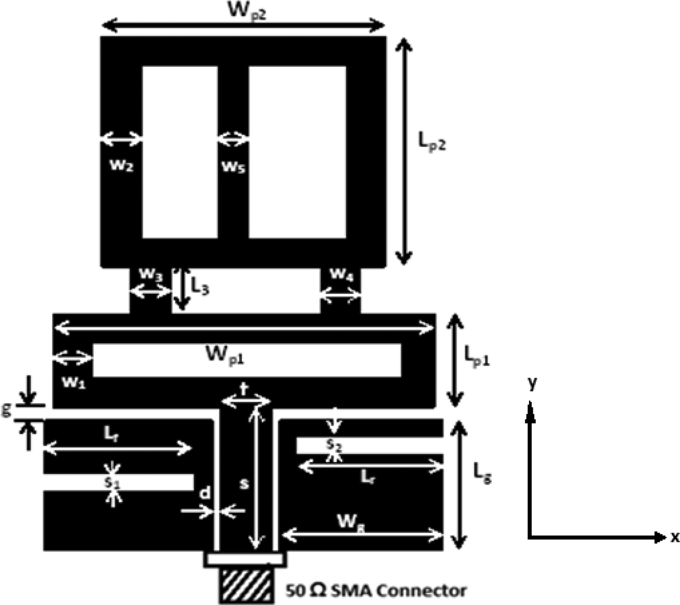
The top view and side view of the final structure of the proposed dualband antenna is depicted in Fig. 1. It consists of metallic double ringed patch layer with a copper thickness of 0.02 mm constructed on a FR4 substrate material of thickness 1.6 mm with dielectric constant (εr) 4.4, and loss tangent (tan δ) value of 0.018. The antenna is excited by a CPW feed which comprises a central strip of length “s” and width “t’. There is a gap between the central strip of CPW feed and either ground plane which is represented as “d’. It is surrounded by two equal finite ground planes, each with dimensions L g × W g. CPW feed lying in the same plane as that of the main patch reduces the design complexity and improves the impedance bandwidth of the antenna. The rectangular slot-shaped defects, with dimensions of L f×s1 and L r × s2, respectively, are etched in both the ground planes of CPW feed to form a DGS (Defected Ground Structure). A rectangular patch of dimensions Lp1 × Wp1 is obtained by using the basic design of transmission line theory [Reference Balanis7], which is then slotted from the center to form a ring structure. The antenna structure is further modified by concatenating another larger ringed patch (L p2 × W p2) to the initial antenna design with the help of two small parasitic strips (L 3 × w 3 and L 3 × w 4).

Fig. 1. Geometry of proposed antenna.
Final modification of the antenna to achieve the desired performance is carried out by partitioning the larger upper ring into two asymmetrical rectangular rings with the help of a vertical strip (Lp 2 × w 5). The final antenna structure, as shown in Fig. 1, is the outcome of different parametric variations applied to the initial configuration of the antenna. The optimized parameters of the designed antenna are summarized in Table 1.
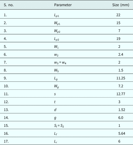
Table 1. Final dimensions for double ringed CPW fed microstrip antenna
A design procedure
The design is based on the principle that slotting a rectangular patch from its center decreases the resonant frequency. Also, as the size of the perforation increases, it reduces the resonance frequency for the same antenna size or it can be said that same resonant frequency is achieved by the smaller ring size. The extent of frequency reduced and the reduction in size depends upon the ratio of outer patch length to the length of the perforation of the patch [Reference Bafrooei19]. The design procedure of the antenna is divided into four steps:
Step 1: Initially a small, CPW fed, single rectangular ring structure is designed to generate a single resonance at 5.2 GHz, offering a bandwidth of 400 MHz for UNII-1/UNII-2 applications.
Step 2: A larger ring is then added to the smaller ring structure to create another resonance at 2.4 GHz for WLAN operating band but distorts the upper-frequency band at 5.2 GHz.
Step 3: DGS are incorporated in the form of rectangular slots in the CPW ground, which create a wide band from 5.25 to 5.65 GHz.
Step 4: Finally, a vertical strip is added to the upper, larger ring to improve the range of higher frequency band to cover the UNII 1(lower) and UNII 2(middle) bands from 5.10 to –5.35 GHz.
Parametric study
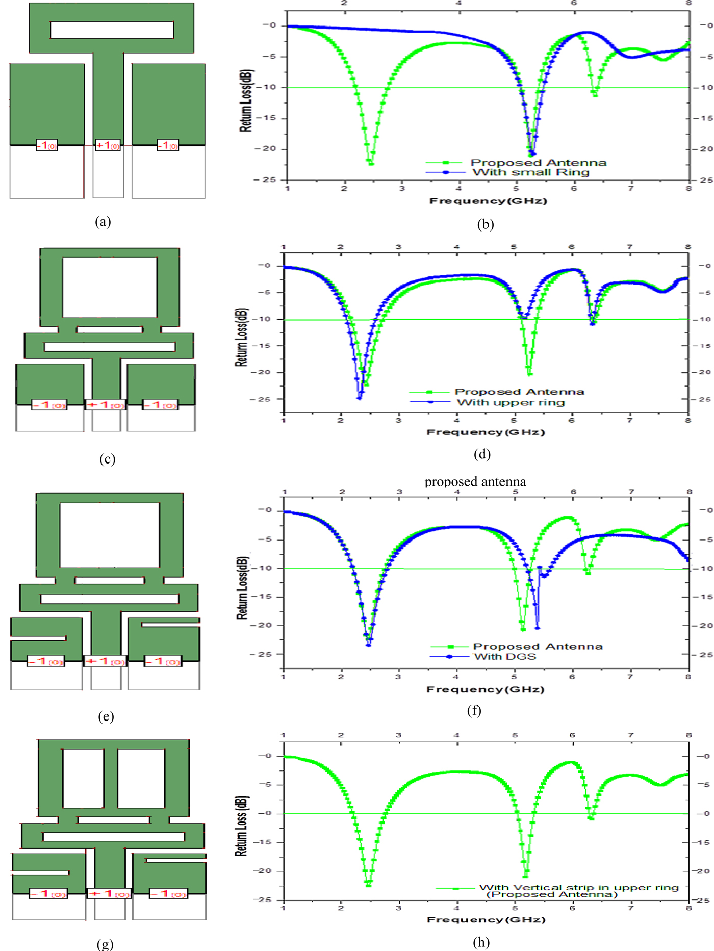
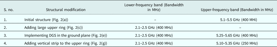
The parametric study is carried out in two steps: first, the structural variations are applied to the antenna by adding various elements to the initial design, then the optimized results for the various bands are obtained by changing its dimensions, which seem to have significant effect on the performance of antenna as regards to its return loss, bandwidth, and radiation pattern. The basic rectangular ring with CPW × feed is taken as the initial structure as shown in Fig. 2(a) and each modification in the initial structure and its corresponding return loss, of the modified structure, is presented in Figs 2(b)–2(h). For comparison the return loss of each structural variation is compared with the final structure.

Fig. 2. Various structural variations applied to the antenna: (a) Initial structure with single ring; (b) Comparative return loss of antenna with single ring and proposed antenna; (c) Adding large upper ring; (d) Comparative return loss of antenna after adding large upper ring and proposed antenna; (e) Implementing DGS in the ground plane; (f) Comparative return loss of antenna with DGS in CPW ground planes and proposed antenna; (g) Adding vertical strip to the upper ring; (h) Comparative return loss of antenna with vertical strip in upper ring and proposed antenna.
Structural variations
Initial structure using single slotted rectangular patch
The initial design consists of a rectangular patch, the initial dimensions of which are calculated using basic design equations based on transmission line theory [Reference Balanis7]. The solid rectangular patch is then slotted from its center to form a ring structure as illustrated in Fig. 2(a). The printed ring antenna has been used earlier to obtain dual-frequency operations [Reference Shafhi and Chamma20]. Increasing the size of the slot, shifts the resonance frequency to lower side, and helps to achieve resonance with a smaller ring size [Reference Bafrooei19].
The antenna is fed by central stripline surrounded by CPW ground plane on either side of it. The comparative return loss of the single ring antenna and the proposed structure is depicted in Fig. 2(b). The return loss curve indicates that the initial design of the antenna is able to provide a single resonant band from 5.1 to 5.5 GHz, offering a bandwidth of 400 MHz for UNII-1/UNII-2 applications.
Effect of addition of large upper ring
A large upper ring is then incorporated into the initial single ringed patch using two small strips as illustrated in Fig. 2(c). The effect of the addition of the large upper ring is examined in terms of return loss parameter (S 11) of the antenna which exhibits two effects on the performance of the antenna. The band at 5.25 GHz which appeared with the base structure, displays a considerable fall in the return loss (from −21 to −10 dB) which can no longer be considered as useful. Also, it generates two bands at 2.4 and 6.4 GHz. Figure 2(d) shows that the band obtained at 2.4 GHz is quite prominent with a significant return loss value of −26 dB bandwidth of 400 MHz (2.1–2.5 GHz) which is more than the required value for WLAN operation at this band. The band obtained at 6.4 GHz does not show a significant return loss and bandwidth.
Effect of implementing DGS in the CPW ground planes
The structure is modified further by incorporating defects, in the form of rectangular slots, in the CPW grounds of the feed to form DGS, as shown in Fig. 2(e). Formation of defected ground structures has a significant effect on 5.25 GHz and 6.4 Hz bands. The band at 6.4 GHz is moved to a lower frequency and combines with 5.25 GHz band to form a single wideband ranging from 5.25 to 5.65 GHz generating a bandwidth of 400 MHz. It remarkably recovers the return loss value to −21 dB as shown in Fig. 2(f). The DGS in CPW ground does not disturb the lower frequency band at 2.4 GHz.
Effect of addition of vertical strip to the upper ring
The final configuration of the proposed antenna is formed by dividing the upper ring into two rings, by placing a vertical strip in the upper ring as shown in Fig. 2(g). The S 11 parameter curve in Fig. 2(h) shows that the use of vertical strip shifts the upper resonance frequency to 5.1 GHz, covering the band in the desired range, from 5.10 to 5.35 GHz, suitable for UNII 1(lower) and UNII 2 (middle) WLAN operation. Another band is seen at 6.4 GHz but with insignificant return loss value of −11 dB. Effective bands covered by the proposed antenna which are important for WLAN applications range from 2.1 to 2.65 GHz and from 5.1 to 5.35 GHz.
The results of the modifications applied to the antenna structure are summarized in the Table 2 presented below:
Table 2. Summary of results obtained after various structural variations
Parametric variations
Effect of variation of length of slots in CPW ground plane
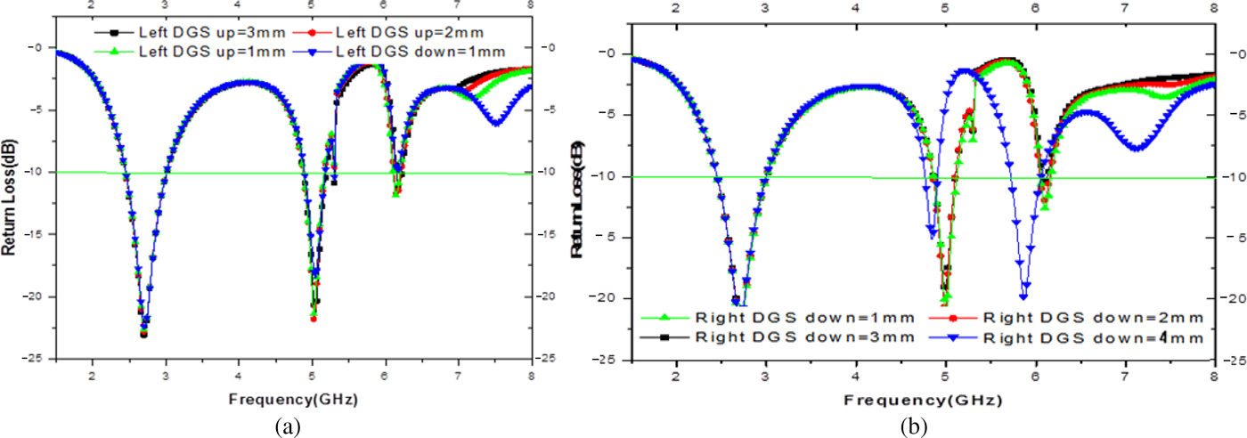
The defects are created in the CPW ground plane to optimize the resonance at 5.15 GHz. The resonance is affected by changing the length, width, and the position of the slots created on the symmetrically placed CPW ground planes. The length of the left-hand side and right-hand side rectangular slots in CPW ground planes are varied to demonstrate their effect on the performance of the proposed antenna. Figures 3(a) and 3(b) shows the effect of varying the length of the left- and right-hand side slot in CPW ground, respectively, on S 11 parameter with reference to frequency.
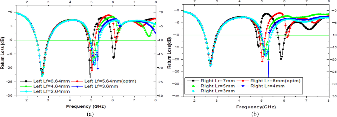
Fig. 3. Effect of variation of slot length of DGS in the (a) left ground plane and (b) right ground plane.
It is apparent from Figs 3(a) and 3(b), that an increase in the length of the rectangular slot from 2.64 to 5.64 mm in left ground plane causes the upper-frequency band to shift to a lower frequency to attain resonance at the anticipated value of 5.15 GHz. Increasing the length of the slot beyond 5.64 mm, shifts the resonance further to a lower frequency and creates another band at a frequency of 6.1 GHz. But the variation in the length of the slot in the left ground plane has little effect on the lower band.
A similar variation is applied to the slot length, L r, in the right-hand side CPW ground plane as presented in Fig. 3(b). The increase of slot length from 3 to 7 mm causes the upper-frequency band to shift from 5.4 to 4.8 GHz frequency with the optimal value at 6 mm to obtain resonance at 5.15 GHz. Further increase in the length of the slot from its optimal value causes the upper band to shift towards lower frequency and also generates additional third band at a frequency of 6.0 GHz. It is seen in simulation results that change in the slot length mainly affects the upper-frequency band and has a negligible effect on the lower-frequency band.
Effect of variation of width of slots in CPW ground plane
The width of the rectangular slots in both the CPW ground planes is then varied to see their effect on the performance of the antenna. As shown in Fig. 4(a), the left-hand side slot width at 0.5 mm generates resonance at the desired value of 5.15 GHz and increasing the value any further distracts the resonance frequency and also decreases the bandwidth.
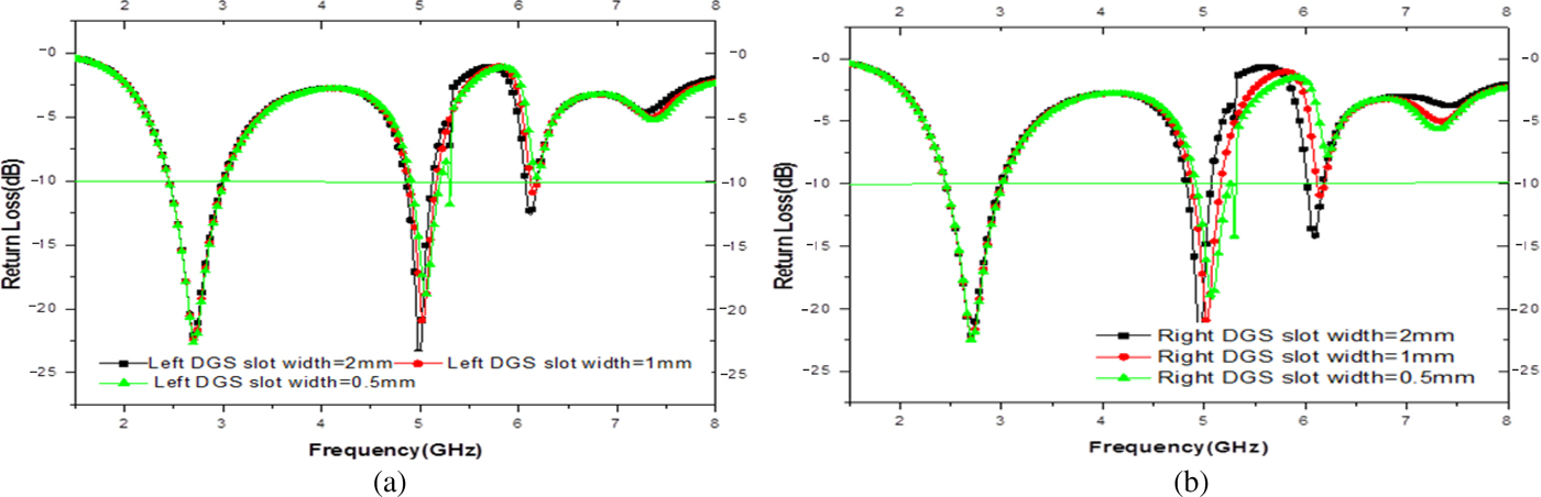
Fig. 4. Effect of variation of slot width of DGS in (a) left ground plane and (b) right ground plane.
Figure 4(b) shows that the slot in the right ground plane is then varied from a value of 0.5–2 mm, and the optimized value of slot width of 2 mm is obtained to achieve the desired band at 5.15 GHz with requisite bandwidth. Increasing it further from 0.5 mm, the bandwidth of the upper band decreases. It does not affect the lower frequency band.
Effect of variation of position of slots in CPW ground plane
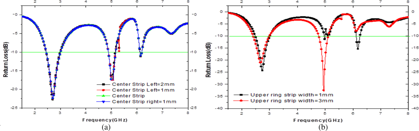
The position of the rectangular slots is varied to see if it affects the performance of the antenna. Initially, the slot in the left CPW ground is positioned at the center i.e. at 6 mm along y-axis and moved up and down different values to see its effect. The position is incremented up by 1, 2, and 3 mm and decremented by 1 mm, as shown in the graph (Fig. 5(a)), but it does not seem to have any significant effect on the return loss or the impedance bandwidth of the antenna.

Fig. 5. Effect of variation of position of slot in (a) left ground plane and (b) right ground plane.
The position of the slot in the right CPW ground significantly influence the antenna performance as shown in Figs 5(a) and 5(b). Initially the slot is positioned at a distance of 1 mm from the upper edge and moved down further to lie at a distance of 2, 3, and 4 mm, which causes deviation in the upper band. For values 1, 2, and 3 mm, almost the same results are obtained at the desired band of operation. At a value of 4 mm, although a remarkable change is produced in the upper band, which gets shifted to 4.75 GHz with the creation of an additional band at 5.8 GHz, this is not as desired. Therefore, we choose 1 mm to be the optimum value for positioning the slot in the right ground plane.
Effect of variation of position and width of the vertical strip in the large upper ring
A vertical strip is placed in the larger upper ring, which divides it into two rings as shown in Fig. 2(f). The position of the vertical strip and its dimension is varied to see its effect on the antenna performance. Initially, it is placed at the center of the upper ring, i.e. 7.5 mm but there is an unwanted dip at 5.2 GHz. Moving the strip 1 mm to the left or towards the right, generates resonance at 5.1 GHz as shown in Fig. 6(a). The simulated results of return loss with respect to frequency, reveal that the variation in the position of the vertical strip from the center does not have a significant impact on either of the two bands. Therefore, we choose to keep the vertical strip at 6.5 mm.

Fig. 6. Effect of variation of (a) position and (b) width of vertical strip in the large upper ring.
The width of the vertical strip is also varied to see its effect on return loss characteristics or the impedance bandwidth of the proposed antenna. As can be seen in the simulated results in Fig. 6(b), when the width of the strip is widened from 1 to 3 mm, the return loss at the upper-frequency band shows considerable improvement from a value of −12 dB at 1 mm width to −32.5 dB at 3 mm width for the required resonant frequency of 5.15 GHz. The optimum value of the strip width is found to be 3 mm.
Results and discussion
The proposed antenna, after simulation, is fabricated using photolithography and wet etching technique and then tested on Agilent's E5071C VNA for its return loss and bandwidth measurements. Radiation pattern measurements are done using an anechoic chamber operating in the frequency range from 2 to 20 GHz with respect to a standard horn antenna with a calibrated gain of 12 dBi. The prototype of the fabricated structure of the antenna is shown in Fig. 7.

Fig. 7. Prototype of the proposed antenna.
The comparative results summarized in Table 3 are obtained between simulated and measured values of return loss and bandwidth as shown in Fig. 8 which shows a good agreement between the two results except for slight variations at some points which could be due to inaccuracies in the fabrication process and loading effect of the connector and cable used for testing purpose. The measured impedance bandwidth of the antenna at two bands is 450 MHz (2.20–2.65 GHz) and 450 MHz (5.0–5.45 GHz) which is good enough to cover the proposed WLAN/UNII bands.
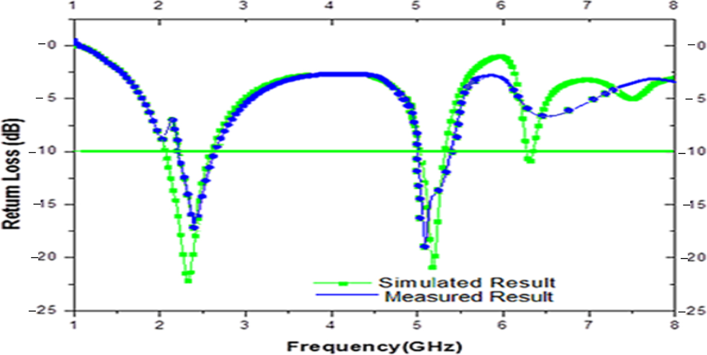
Fig. 8. Comparative plot of simulated and measured return loss of proposed antenna.
Table 3. Summary of the measured and simulated results of the proposed antenna
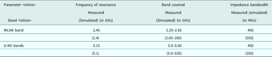
Figure 9 shows the simulated and measured gain across the two bands of the proposed antenna with respect to frequency. It exhibits considerable gain values in both operating bands. For the lower band, the antenna has a maximum radiation gain of about 5.5 dBi whereas for the higher band, the antenna gain is nearly 4.9 dBi.
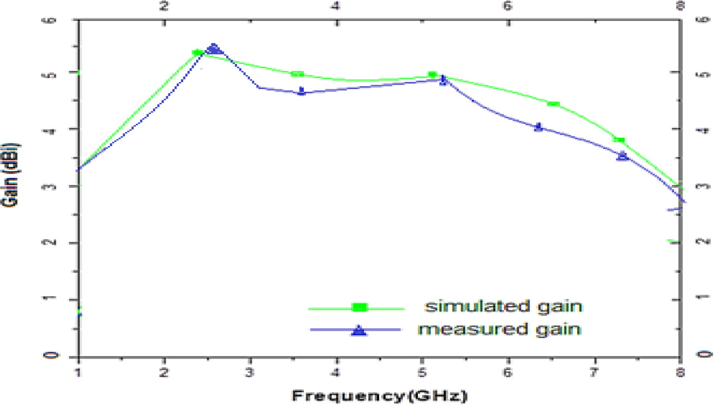
Fig. 9. Comparative plot of simulated and measured gain of proposed antenna.
Figures 10(a) and 10(b), 11(a) and 11(b) show the comparison of simulated and measured azimuthal and elevation power pattern measurements of the antenna at the center frequencies of the two bands at 2.45 GHz and at 5.15 GHz, respectively. A variation from the omnidirectional pattern can be seen in the azimuthal plane, whereas, an exact pattern of figure of eight is represented in the elevation plane. The radiation patterns are stable are over the two operating frequency bands of the antenna.
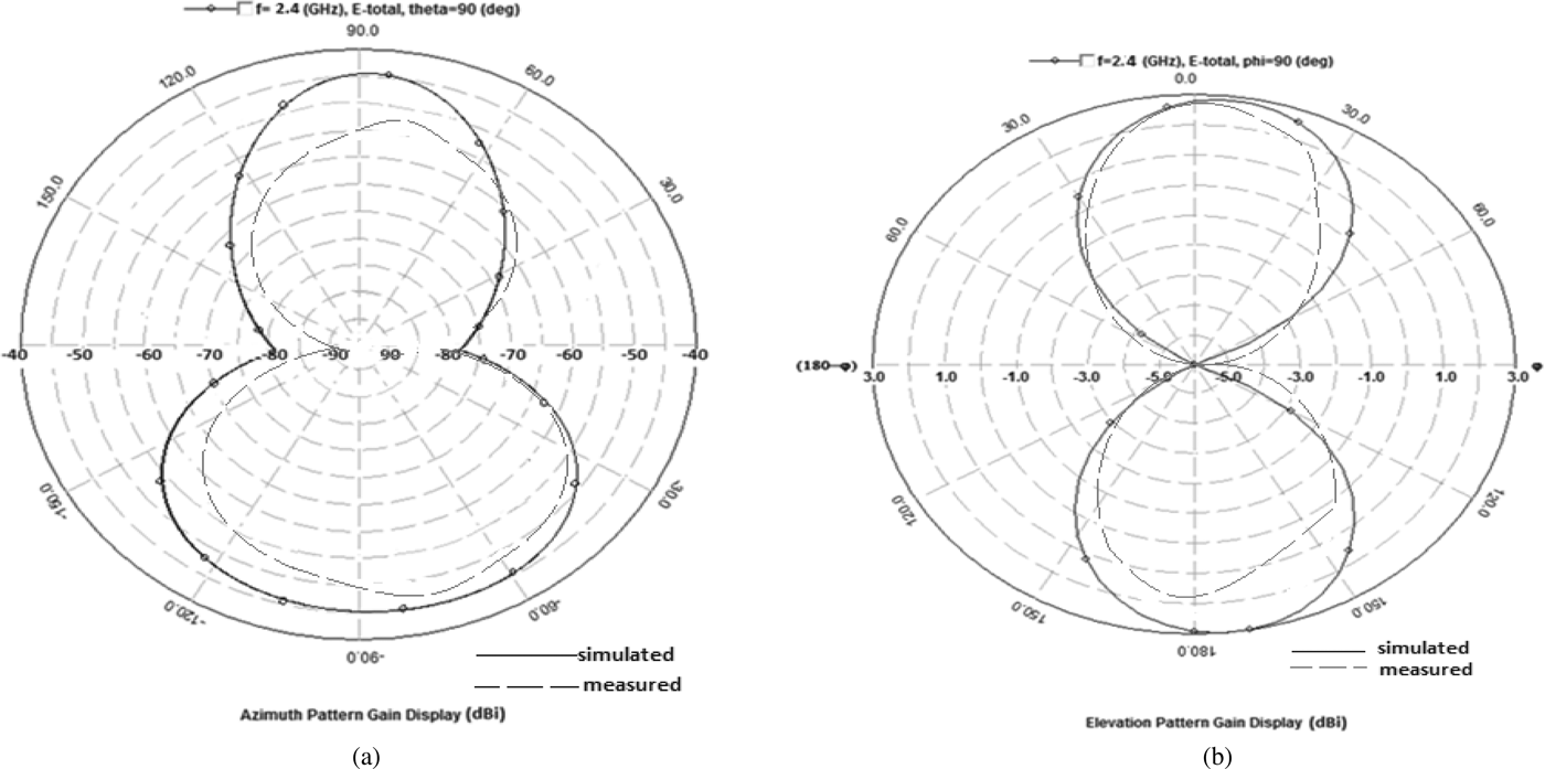
Fig. 10. Radiation pattern plot of antenna in (a) Azimuthal plane and (b) Elevation plane at 2.4 GHz.
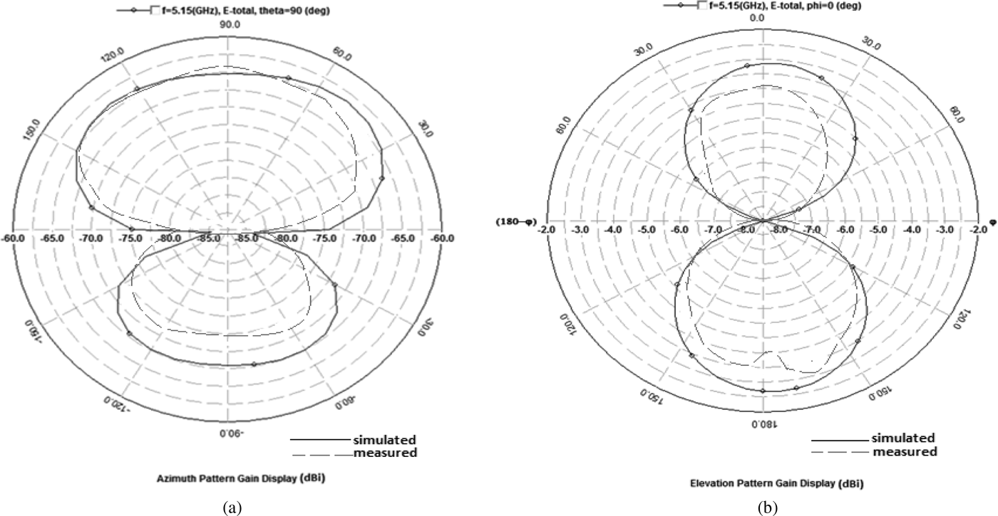
Fig. 11. Radiation pattern plot of antenna in (a) Azimuthal plane and (b) Elevation plane at 5.15 GHz.
In pattern measurement, the simulation values are somewhat different from the measurement values due to the ideal environment considered in simulation whereas the measured results are produced in the anechoic chamber in which the environment is near to ideal but not as much as in simulation. In actual measurements, the errors may arise due to imperfect leveling, fabrication tolerances, and measurement limitations also.
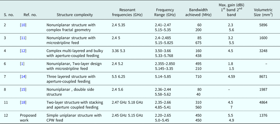
A comparison of the proposed structure with the existing antennas is presented in Table 4.
Table 4. Comparison of the proposed antenna parameters with several existing designs

From the comparison Table 4, it can be interpreted well that the proposed antenna is a simple, small sized, uniplanar, CPW fed structure with high gain and wide bandwidth at both the bands (WLAN and UNII-1/UNII-2).
Conclusion
In this paper, a planar CPW fed dual ring antenna with DGS is designed and fabricated to work in the WLAN bands. It provides permissible return loss over the two frequency bands ranging from 2.20 to 2.65 GHz at the lower frequency band and from 5.0 to 5.45 GHz at the higher band, which is verified by experimental results. With the insertion of slots into the CPW ground planes and division of larger ring into two by a vertical strip, the proposed antenna can provide sufficient impedance bandwidths and suitable radiation characteristics over the 2.4/5.2 GHz WLAN bands. The WLAN band has an impedance bandwidth of 450 MHz with a return loss of −16 dB and maximum gain value of 5.5 dBi. At the UNII bands, the impedance bandwidth of 450 MHz is achieved with a return loss of −19 dB and gain value of 4.9 dBi at the maxima point.
 Geetanjali Singla received her Masters in Electronics and Communication Engineering from BBSBEC, Fatehgarh Sahib in 2010 and completed her Ph.D. degree from Thapar Institute of Engineering and Technology. Presently, she is a lecturer at Thapar Institute of Engineering and Technology, Patiala. Her main research interests are design and optimization of Microstrip antenna, Multiband, and wideband antenna, and Wireless communication networks. She has published many papers in journals and conferences on Microstrip antenna and wireless communications networks.
 Rajesh Khanna received a B.Sc. (Engg.) degree in ECE in 1988 from REC, Kurukshetra and M.E. degree in 1998 from IISc., Bangalore. He was with Hartron R&D center till 1993. Until 1999, he was in AIR as ASEngg. Presently, he is working as Professor in the ECE Deptt. at Thapar Institute of Engineering and Technology, Patiala. He has published 80 papers in National and International journal/Conferences. He has worth Rs 1.5 crore projects to his credit. His main research interest includes antennas, Wireless Communication, MIMO, and FFT.
 Davinder Parkash was born in Haryana, India in 1976. He received B.Tech., M.Tech., and Ph.D. degree from the Deptt. Of Electronics and Communication Engineering at Kurukshetra University, Kurukshetra and NIT, Kurukshetra and Thapar University, Patiala in 1999, 2007, and 2015, respectively. He is currently working as a Professor at University Institute of Engineering, Chandigarh University, Gharuan. He received the “Young Scientist Award” from the Governor of Punjab (India). He has published more than 60 papers in national and international journals/conferences. His main research interest includes the analysis and design of microstrip antenna, DGS technique, RFID antenna, and Wireless Communication.