I. INTRODUCTION
Dielectric resonator antenna (DRA) is considered to be one of the front-line antenna model now-a-days. From the day of its invention [Reference Long, Mcallister and Shen1], it has brought keen attention in antenna researchers’ community. This is only because of its several performance specifics such as wide bandwidth, high radiation efficiency, and low loss as well as geometrical specifics such as more design flexibility than the conventional printed antennas [Reference Luk and Leung2, Reference Petosa3]. It has been extensively used for different applications in microwave engineering domain [Reference Dash, Khan and De4]. Out of these, the usability of X-band is quite prevalent in civil as well as in military domain [Reference Sahu, Singh, Singh and Tripathi5]. In general, it requires compact, wideband, high-gain, low-loss, and high-efficiency characteristics [Reference Petosa3]. In reference to [Reference Hwang, Zhang, Luk and Yung6], DRA satisfies the desired requisites except for high gain as it deals with an average gain of ~5 dB. Different techniques such as stack [Reference Hwang, Zhang, Luk and Yung6, Reference Pan and Zheng7], electromagnetic band gap (EBG) [Reference Denidni, Coulibaly and Boutayeb8], surface-mounted horn [Reference Nasimuddin and Esselle9], mode [Reference Petosa and Thirakoune10, Reference Guha, Banerjee, Kumar and Antar11], reflector [Reference Ali, Zakariya, Baharudin, Khir, Baba and Adz12], and array [Reference Nikkhah, Kishk and Rashed-Mohassel13], etc. have been proposed for improvement of the gain. However, improving the gain of compact size DRA without disturbing the bandwidth is quite challenging.
In view of gain improvement with a compact structure and null effect on other performances superstrate loading concept can be considered as an ultimate alternative. This technique has been widely used for the gain improvement of microstrip antennas [Reference Vaidya, Gupta, Mishra and Mukherjee14, Reference Li, Lei and Liang15]. In case of DRAs, the superstrate-loading concept is very much limited [Reference Coulibaly, Nedil, Talbi and Denidni16–Reference Ge, Sun, Chen and Chen21], such as frequency selective surface (FSS) superstrate [Reference Coulibaly, Nedil, Talbi and Denidni16, Reference Choubar, Gupta, Farahani, Sebak and Denidni17], metamaterials superstrate [Reference Sahu, Aggarwal, Tripathi and Singh18], metal superstrate [Reference Dutta, Guha, Kumar and Antar19], transparent non-metallic superstrate [Reference Coulibaly, Nedil, Talbi and Denidni20], and stacked dielectric superstrate [Reference Ge, Sun, Chen and Chen21]. Generally, FSS and metamaterials structures are electrically complex as they are made in the form of array and nanometers scale [Reference Balanis22]. Hence, they need high precision during fabrication [Reference Cui, Smith and Liu23]. In this context [Reference Coulibaly, Nedil, Talbi and Denidni16–Reference Sahu, Aggarwal, Tripathi and Singh18], also deal with the same issues. In [Reference Dutta, Guha, Kumar and Antar19], the authors have introduced a metal sheet as a superstrate for improving the gain. Though the approach is good, the overall size of designed superstrate, i.e. 96 × 96 × 0.3 mm3, may create application restraint. The overall larger superstrate size, i.e. 34 × 34 × 4.5 mm3, is the main constraint of the stacked superstrate in [Reference Ge, Sun, Chen and Chen21] too.
Here, in this proposed work, the authors have developed a simple conical DRA covered by a narrow transparent lightweight dielectric superstrate (no FSS/EBG/patch) for 42.85% gain improvement and tapered ground plane for 68.92% bandwidth improvement. The uniqueness of the proposed work can be considered as: (i) incorporation of lighter weight narrow dielectric superstrate for gain improvement, which is rarely proposed in the existing open literature; (ii) integration of tapered ground plane for bandwidth enhancement; (iii) overall compact geometry (not array, as in [Reference Nikkhah, Kishk and Rashed-Mohassel13]); (iv) economic and ease of fabrication; and (v) high co-to-cross-polarization ratio. This paper is organized as follows: the proposed antenna geometry is described in Section II, followed by geometry optimization and analysis in Section III. Prototype fabrication and result validation are discussed in Section IV. Finally, the conclusion followed by references is discussed in Section V.
II. PROPOSED ANTENNA GEOMETRY
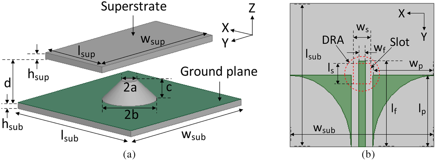
Figure 1 depicts the proposed antenna geometry. It has three main parts: a conical dielectric resonator (ε rd = 10), a dielectric ground plane substrate (ε rsub = 4.4, tanδ = 0.02), and a dielectric superstrate substrate (ε rsup = 4.4, tanδ = 0.02). The conical dielectric resonator has upper radius a = 2 mm, lower radius b = 7 mm, and height c = 5 mm. The dielectric ground plane substrate has length l sub = 40 mm, width w sub = 40 mm, and thickness h sub = 1.6 mm. The dielectric superstrate has length l sup = 40 mm, width w sup = 20 mm, and thickness h sup = 1.6 mm. The substrate is placed at an air gap d = 7 mm from the ground plane substrate. For coupling purpose, a rectangular slot (l s × w s = 7 × 5 mm2) is made on the upper side of the ground plane substrate with a 50 Ω microstrip feed line (l f × w f = 24 × 2 mm2) on the other side of the substrate. A set of tapered patch is used on either side of the microstrip feed line for performance improvement. This proposed antenna geometry is designed and simulated using HFSS v13.0 [24].

Fig. 1. Schematic diagram of the proposed dielectric resonator antenna, (a) 3D view, (b) bottom view of ground plane substrate (the dotted lines indicating DRA and slot are made on top side of the ground plane. Here l sub = w sup = 40, l sup = 40, w sup = 20, h sub = h sub = 1.6, l f = 24, w f = 2, l s = 7, w s = 5, l p = 20, w p = 17, a = 2, b = 7, c = 5, d = 7. Further all dimensions are in millimeter).
III. GEOMETRY OPTIMIZATION AND ANALYSIS
The proposed DRA geometry is optimized in two steps: step 1 deals with optimization of the DR dimensions and coupling-slot dimensions. The superstrate and ground plane are then optimized in steps 2 and 3, respectively.
A) Step 1: DR dimensions and coupling-slot dimensions optimization
As per [Reference Luk and Leung2], a cylindrical DR has one degree of freedom (two controlling parameters, i.e. radius and height). On the other hand, in cone, the number of controlling parameters increased to three (i.e., upper radius, lower radius, and height), which is another advantage from modeling point of view. Hence, in order to find out the optimized cone dimension, upper and lower radius as well as height (as these parameters generally affect the Q-factor [Reference Luk and Leung2]) of the cone are taken into consideration, and their effects on antenna performance in terms of bandwidth and gain are observed carefully (Fig. 2).

Fig. 2. Effect on S11 and gain (a) variation due to DR-upper radius at fixed b = 5 mm and c = 5 mm, (b) variations due to DR-lower radius at fixed a = 2 mm and c = 5 mm, and (c) variations due to DR-thickness at fixed a = 2 mm and b = 7 mm.
The effect of varying the upper radius (a) of the cone on resonance frequency shift as well as on gain is shown in Fig. 2(a). It is clear that the resonance matching is improving from −18 to −28 dB by varying the upper radius (0.03λ 0 ≤ a ≤ 0.13λ 0). For the same variations in the radius, the resonance frequency is also shifting (from 9.3 to 8.0 GHz) in lower side indicating the frequency reconfigurability. In comparison to resonance variation, the gain value does not vary much (Fig. 2(a)). Thus, the upper radius is optimized here as a = 0.06λ 0 to achieve the impedance bandwidth of 6.79% with a peak gain of 4.88 dBi. Similarly, the lower radius of the cone (i.e., b) is varied between 0.16λ 0 ≤ b ≤ 0.26λ 0, and finally, it is optimized as b = 0.23λ 0 for achieving the impedance bandwidth of 7.91% with a peak gain of 5.32 dBi as described in Fig. 2(b). In this optimization, the upper radius remains constant at a = 0.06λ 0. Finally, the height of the cone (i.e., c) is varied between 0.13λ 0 ≤ c ≤ 0.23λ 0 (Fig. 2(c)) and found to be better at c = 0.16λ 0, i.e. the initial value taken during optimization of a and b. Hence, the results are similar as of previous optimization (of radius b).
For coupling of the DR, a rectangular slot of size l s × w s was inserted at the center of top side of the ground plane. Therefore, post DR optimization, to observe the effect of the slot, both the slot length (l s ) and slot width (w s ) are varied in between 0.16λ 0 ≤ l s ≤ 0.3λ 0 and 0.1λ 0 ≤ w s ≤ 0.23λ 0, respectively. These variations are plotted in Figs 3(a) and 3(b), respectively. The resonance frequency of the antenna is not varying here in both the cases as plotted in Figs 3(a) and 3(b). It may be because of the fact that in general, the mode of operation of the DR depends upon its dimensions, but not upon the ground plane/slot dimension [Reference Luk and Leung2, Reference Petosa3]. Thus, the slot length (l s ) and slot width (w s ) are optimized as: l s = 0.23λ 0 and w s = 0.16λ 0 to achieve an impedance bandwidth of 9.46% with a peak gain of 5.32 dBi. The antenna having conventional microstrip feed, optimized in this section, is denoted as DRA #1.

Fig. 3. Effect on S11 and gain (a) variation due to slot-length (l s ) at fixed w s = 0.16λ 0 (b) variation due to slot-width (w s ) at fixed l s = 0.23λ 0.
B) Step 2: Superstrate optimization
The distinctive surface current distribution required to achieve desired performance characteristics can be accompolished by using a superstare [Reference Coulibaly, Nedil, Talbi and Denidni16, Reference Dutta, Guha, Kumar and Antar19]. There are several types of superstrates such as: semi-transparent non-metallic superstrate [Reference Coulibaly, Nedil, Talbi and Denidni16–Reference Sahu, Aggarwal, Tripathi and Singh18], non-transparent metallic superstrate [Reference Dutta, Guha, Kumar and Antar19], and transparent non-metallic superstrate [Reference Coulibaly, Nedil, Talbi and Denidni20]. For the proposed work, authors have considered a solid transparent non-metallic superstrate. Its optimization is being discussed in this section.
An FR-4 (ε rsup = 4.4) substrate sheet of 1.6 mm thickness is placed as a superstrate at height d from the ground plane substrate. Thus, the superstrate–substrate length (i.e., l sup ) and width (i.e., w sup ) are varied between 10 mm ≤ l sup ≤ 40 mm and 10 mm ≤ w sup ≤ 40 mm, respectively. The gap between the superstrate–substrate and the ground plane substrate (i.e., d) is also varied between 6 mm ≤ d ≤ 9 mm (i.e., 0.2λ 0 ≤ d ≤ 0.3λ 0). The variations in gain total for different values of l sup and w sup are depicted in Fig. 4(a), whereas the variations in S 11 and gain total for different values of d are plotted in Fig. 4(b). The three-dimensional view shown in Fig. 4(a) indicates that the gain of the antenna remains almost constant for different l sup = w sup (i.e., ~6.2 dBi at θ = 0°, φ = 0°), whereas it increases almost linearly with increase of different l sup ≠ w sup . It can be concluded that the gain increases when the length of the superstrate is oriented in the direction of antenna polarization. Thus, l sup = 40 mm, w sup = 20 mm, and d = 7 mm are optimized to achieve a peak gain of 6.65 dBi with 10.73% impedance bandwidth. The antenna with superstrate, optimized in this section, is considered as DRA #2.

Fig. 4. (a) Gain total variation of the antenna for different combinations of lsup and wsup (at d = 7 mm and θ = 0°, φ = 0°), (b) effect of air-gap height on bandwidth and gain.
C) Step 3: Ground plane optimization
The dimensions of DR as well as coupling slot are optimized in step 1 with a conventional microstrip feed line on the bottom side of the ground plane substrate. The superstrate dimensions are then optimized in step 2. In this step, the microstrip feed line structure (Fig. 5(a)) is further modified in twofold: one is based on microstrip feed line with two parasitic conducting patches (Fig. 5(b)), and another is based on microstrip feed line with two parasitic conducting tapered patches (Fig. 5(c)). For making it convenient for comparison, the ground planes shown in Figs 5(a)–5(c) are denoted as ground plane 1, ground plane 2, and ground plane 3, respectively. The antenna with superstrate and ground plane 3 is considered as DRA #3. The E-field distributions for these three ground planes are shown in Figs 6(a)–6(c), respectively.

Fig. 5. Different modified ground planes, (a) with only feed, (b) with feed and rectangular parasitic patch (c) with feed and tapered parasitic patch.

Fig. 6. E-filed distribution in the top side of ground planes, (a) Ground Plane-1, (b) Ground Plane-2, (c) Ground Plane-3.
The proposed DRA with ground plane 1 gives an impedance bandwidth of 10.73% with 6.65 dBi peak gain (Fig. 7(a)). To impose the parasitic coupling, a set of rectangular patches (each of l p × w p = 0.66λ 0 × 0.56λ 0) is suspended on either side of the feed line (Fig. 5(b)). The E-field becomes comparatively stronger (Fig. 6(b)) than without patch (ground plane 1) (Fig. 6(a)). The E-field near to the edge of the substrate could not couple the DR actively. Thus, the bandwidth decreased to 8.8%. However, the gain of the antenna remains almost same (~6.68 dBi) as of previous case. This indicates further refinement of these parasitic patches for performance improvement.

Fig. 7. Variation of S11 and gain total, (a) for three different ground planes, (b) for three different stages of DR-antennas.
For further improvement, the suspended parasitic patches are made tapered (Fig. 5(c)) by considering two ellipses – each of major axis (l p ) = 0.66λ 0 and minor axis (w p ) = 0.56λ 0 (i.e., Tool ellipse-1/Tool ellipse-2 (Fig. 5(c))) are taken and kept centering at the bottom edge corner of the rectangular patch, so that 1/4th of each ellipse covers some part of the rectangular patch (Fig. 5(c)). Finally, using HFSS v13.0 [24] subtract tool, these elliptical shapes are subtracted from respective rectangular patches, which resulted a tapered patch. This modification further strengthens the E-field on the top side ground plane along the feed line as well as the tapered patch (Fig. 6(c)). This configuration creates additional resonance in the lower frequency and abruptly enhances the bandwidth up to 15.48%, with an improved peak gain of 7.25 dBi. This superstrate and ground plane 3-based antenna is considered as DRA #3. The S 11 and gain variations for DRA #3 as well as two already described DRAs (DRA #1 and DRA #2) are depicted in Fig. 7(b). The performance comparison of DRA with these three ground planes are compared and summarized in Table 1, which is self-explanatory. Post optimization of DRA #3, the E-field distribution inside the DR is shown in Fig. 8(a), which signifies the HEM11δ mode [Reference Petosa3]. The E- and H-fields on the superstrate are shown in Figs 8(b) and 8(c), respectively.

Fig. 8. Field distribution, (a) E-field in cone indicates HEM11δ mode, (b) E-field in superstrate, (c) H-Field in superstrate.
Table 1. Comparison of effect of conducting sheets on DRAs’ performance.

IV. PROTOTYPE FABRICATION AND RESULT VALIDATION
The proposed work is validated by fabricating an antenna prototype based on DRA #3, and the snapshot of the same is depicted in Fig. 9. Dielectric FR-4 sheet (ε r = 4.4) is used here for the ground plane substrate as well as superstrate. The photo lithography etching process is used for making the two PCBs – one for ground plane and another for superstrate. Automatic CNC machining is applied to make a dielectric cone of a = 2 mm, b = 7 mm, and c = 5 mm from Eccostock HiK rod (ε r = 10). With the help of adhesive glue, the dielectric resonator is made fix on the ground plane. The superstrate is kept above the ground plane at an air gap d = 7 mm with the help of some non-conducting material (foam spacers) of ε r ~ 1. Then, the structure is characterized by using vector network analyzer.

Fig. 9. Fabricated prototypes, (a) bottom-view, (b) side-view.
The measured parameters (both S 11 and gain total) of the fabricated DRA #3 are compared with their simulated counterparts in Figs 10(a) and 10(b), respectively. Though the measured one's resonance shifts from lower to higher frequency, there is still very good matching in the trend. The variation in the resonance is because of the invisible air gap between the ground plane and dielectric resonator, and the unconsidered soldering materials. The measured gain reaches peak 7.6 dBi (Fig. 10(b)) with average 0.5 dBi gain variation with the simulated one, which is negligible. In addition to this, the simulated radiation efficiency of the optimized antenna (i.e., DRA #3) is depicted in Fig. 10(b). It shows that the efficiency varies between 0.76 and 0.88 over the matching bandwidth with an average value of 0.82. Though DRA gives better efficiency than other antennas, i.e. >95% [Reference Luk and Leung2, Reference Petosa3], the variation and comparatively less efficiency of the proposed antenna can be attributed to the lossy dielectric sheet (FR-4) taken as a ground plane substrate.

Fig. 10. Measured and simulated results, (a) S11 variations, (b) gain total variation.
The overall performance comparison of three DRAs is depicted in Table 2, which is self-explanatory. The general outcome of this superstrate and tapered patch/ground plane-based DRA (DRA #3) can be summarized as: (i) 68.92% improvement in the percentage bandwidth, i.e. 1.2 GHz; (ii) 42.85% improvement of the gain total with a peak value of 7.6 dBi; (iii) operating in hybrid HEM11δ mode; (iv) introduction of much compact and lightweight dielectric superstrate in comparison to [Reference Coulibaly, Nedil, Talbi and Denidni16] and [Reference Dutta, Guha, Kumar and Antar19]; and (iv) no complicated patch or geometry (FSS/metamaterial) as in [Reference Coulibaly, Nedil, Talbi and Denidni16–Reference Sahu, Aggarwal, Tripathi and Singh18], which reduces the simulation time and improves fabrication feasibility.
Table 2. Comparison of three different DRAs.

The radiation patterns are measured for two resonating frequencies, i.e. at 7.7 GHz (Figs 11(a) and 11(b)) and 8.15 GHz (Figs 11(c) and 11(d)). Despite the presence of unconsidered foam spacers, the measured gain radiation patterns seem to be more accurate like simulated one in E-plane as well as in H-plane (Fig. 11). The observed co-to-cross-polarization ratios were as follows: 50.48:1 (H-plane) and 2:1 (E-plane) at 7.6 GHz, and 44.52:1 (H-plane) and 1.31:1 (E-plane) at 8.15 GHz. Post characterization, the proposed model is compared with some existing literatures [Reference Sahu, Singh, Singh and Tripathi5, Reference Hwang, Zhang, Luk and Yung6, Reference Petosa and Thirakoune10, Reference Ali, Zakariya, Baharudin, Khir, Baba and Adz12] in Table 3. This comparison is purely based on different techniques, physical compactness, and performances, which shows its advantages over those exiting ones.

Fig. 11. Measured and simulated gain radiation patterns, (a) E-plane at 7.70 GHz, (b) H-plane at 7.70 GHz, (c) E-plane at 8.15 GHz, (d) H-plane at 8.15 GHz.
Table 3. Comparison of proposed models with some existing models.

r, radius; h, height of the cylindrical dielectric resonator.
* Directivity.
V. CONCLUSION
In this communication, the bandwidth and gain improvement of a conical DRA with a narrow dielectric superstrate have been proposed. It has been demonstrated that by reducing the superstrate dimension opposite to the direction of antenna polarization possesses low profile, compact size, and high gain without much altering the other performance of the antenna. In addition to this, a set of tapered patch (ground plane 3) has been placed on either side of the microstrip feed line for bandwidth and reasonable gain improvement. The gain and the impedance bandwidth in the demonstrated antenna (DRA #3) have been improved by 42.85% and 68.92%, respectively. High co-to-cross-polarization ratio (50.48:1) has been found in the H-plane at 7.6 GHz, while 44.52:1 in the H-plane at 8.15 GHz, respectively. The proposed antenna geometry can be a suitable candidate for X-band applications. Thus, proper scope should be arranged for the suitable utilization of this proposed idea. However, further miniaturization of this geometry would be much valuable.
 Sounik Kiran Kumar Dash received his B.Tech degree in the stream of Electronics and Communication Engineering from Centurion University of Technology and Management, Bhubaneswar, India in 2013 and M.Tech degree with specialization of Communication System Engineering from KIIT University, Bhubaneswar, India in 2015. At present he is working as a full time Ph.D. Scholar at National Institute of Technology Silchar, India. His current research interests include Dielectric Resonator Antennas (DRAs), MIMO Antennas, Reconfigurable Antennas, Numerical Methods in Electromagnetics, and Neural Networks. He has authored or co-authored eight research papers in international journals and international conferences/symposiums proceedings of repute. He is an active student member IEEE APS/SPS/EDS (USA), member IAENG (China).
 Taimoor Khan obtained his Polytechnic Diploma in Electronics Engineering, Bachelor Degree in Electronics and Communication Engineering and Master Degree in Communication Engineering from Board of Technical Education, Lucknow, India, The Institution of Engineers (India) Kolkata, India and Shobhit University Meerut, India in the year 2001, 2005 and 2009, respectively. He was Awarded Ph.D. Degree in Electronics and Communication Engineering from National Institute of Technology Patna, India in the year 2014. Presently, he is working as an Assistant Professor at National Institute of Technology Silchar, India. Prior to joining this institute, he served Delhi Technological University, Delhi, India as Assistant Professor more than two years, Netaji Subhas Institute of Technology Patna for more than a year and more than nine years to Shobhit University, Meerut as Lab Instructor, Lecturer and Assistant Professor. During September–December 2016, Dr. Khan has also worked as Visiting Assistant Professor in Telecommunication Field of Study at Asian Institute of Technology Bangkok, Thailand. His research interest includes Microstrip Antennas, Microwave Engineering and Electromagnetics and Artificial Intelligence Paradigms in Electromagnetics. He has published over twenty five research papers in international journals and international/national conference proceedings of repute. He is an active senior member of IEEE (USA), life member of IEI (India) and life member of IAE (USA).
 Binod Kumar Kanaujia received his Bachelor Degree in Electronics Engineering from KNIT Sultanpur, India in 1994. He did his Master Degree from Department of Electronics Engineering, Indian Institute of Technology Banaras Hindu University, Varanasi, India in 1998. He was awarded his Ph.D. Degree from Department of Electronics Engineering, Indian Institute of Technology Banaras Hindu University, Varanasi, India in 2004. He has been awarded Junior Research Fellowship by UGC Delhi in the year 2001–02 for his outstanding work in electronics field. Presently, Dr. Kanaujia is working as Professor in the School of Computational and Integrative Sciences, Jawaharlal Nehru University, New Delhi since August, 2016. Before joining Jawaharlal Nehru University, he had been in Department of Electronics & Communication Engineering in Ambedkar Institute of Advanced Communication Technologies & Research (formerly Ambedkar Institute of Technology), Delhi as a professor since Feb. 2011 & Associate Professor (2008–2011) and Dr. Kanaujia held the positions of Lecturer (1996–2005) and Reader (2005–2008) in the Department of Electronics & Communication Engineering and also as Head of the Department in the M.J.P. Rohilkhand University, Bareilly, India. Prior to his career in academics, Dr. Kanaujia had worked as Executive Engineer in the R&D division of M/s UPTRON India Ltd. He has keen research interest in design and modelling of microstrip antenna, dielectric resonator antenna, left handed metamaterial microstrip antenna, shorted microstrip antenna, ultra wideband antennas, reconfigurable and circular polarized antenna for wireless communication. He has been credited to publish more than 150 research papers with more than 430 citations with h-index of 12 in peer-reviewed journals and conferences. He had supervised 50 M.Tech and 08 Ph.D. research scholars in the field of microwave engineering. He is a reviewer of several journals of international repute i.e. IET Microwaves, Antennas & Propagation, IEEE Antennas and Wireless Propagation Letters, Wireless Personal Communications, Journal of Electromagnetic Wave and Application, Indian Journal of Radio and Space Physics, IETE Technical Review, International Journal of Electronics, International Journal of Engineering Science, IEEE Transactions on Antennas and Propagation, AEU-International Journal of Electronics and Communication, International Journal of Microwave and Wireless Technologies, etc. Dr. Kanaujia had successfully executed 04 research projects sponsored by several agencies of Government of India i.e. DRDO, DST, AICTE and ISRO. He is also an active member of several academic and professional bodies i.e. IEEE, Institution of Engineers (India), Indian Society for Technical Education and The Institute of Electronics and Telecommunication Engineers of India.