Introduction
Recent advances in wireless communication systems have increased the demand for microwave passive [Reference Chiu, Yum, Xue and Chan1–Reference Song, Yifang, Maoyu, Yu and Yong13] circuits with compact size to propose ultra-wideband [Reference Chiu, Xue and Chan2, Reference Hu, Kaijun and Yong5, Reference Tang, Xianqi, Yong and Kaijun9, Reference Wang, Wang and Zhang14–Reference Yang, Luo, Dong and Yang17]. As one of the key devices, power divider is widely studied by scholars. More compact circuit size with wider bandwidth has become an important research direction. Wilkinson divider as the most widely used power divider has good isolation performance [Reference Wilkinson18], but its bandwidth cannot meet the demand of ultra-wideband. In order to achieve ultra-wideband, some ultra-wideband power dividers have been developed [Reference Chiu, Yum, Xue and Chan1, Reference Chiu, Xue and Chan2, Reference Wang, Wang and Zhang14, Reference Zhuge, Song and Fan16]. In [Reference Sung-Won, Kim, Choi Kwan, Park and Ahn19], a design formula of multi-section power divider is derived to obtain wide isolation performance. However, this method requires a larger circuit size and more resistance, which are not conducive to integration. Recently, a few ultra-wideband power dividers [Reference Wang, Wang and Zhang14, Reference Zhang and Liu20] based on the coupling structure were developed in order to achieve a high-frequency selectivity characteristics.
In this paper, a compact power divider is presented with ultra-wideband bandpass response. The nested structure makes the circuit more compact. Open-circuit microstrip lines are loaded at the ends of parallel-coupled lines to achieve ultra-wideband and high-frequency selectivity. Two resistors are designed to improve the isolation within the passband. Through the even–odd mode analysis, the relationship between the two isolation resistances is demonstrated. To verify the validity of the proposed design concept, an ultra-wideband power divider is fabricated and measured. Measured results agree well with the simulated ones.
Structure, analysis, and design
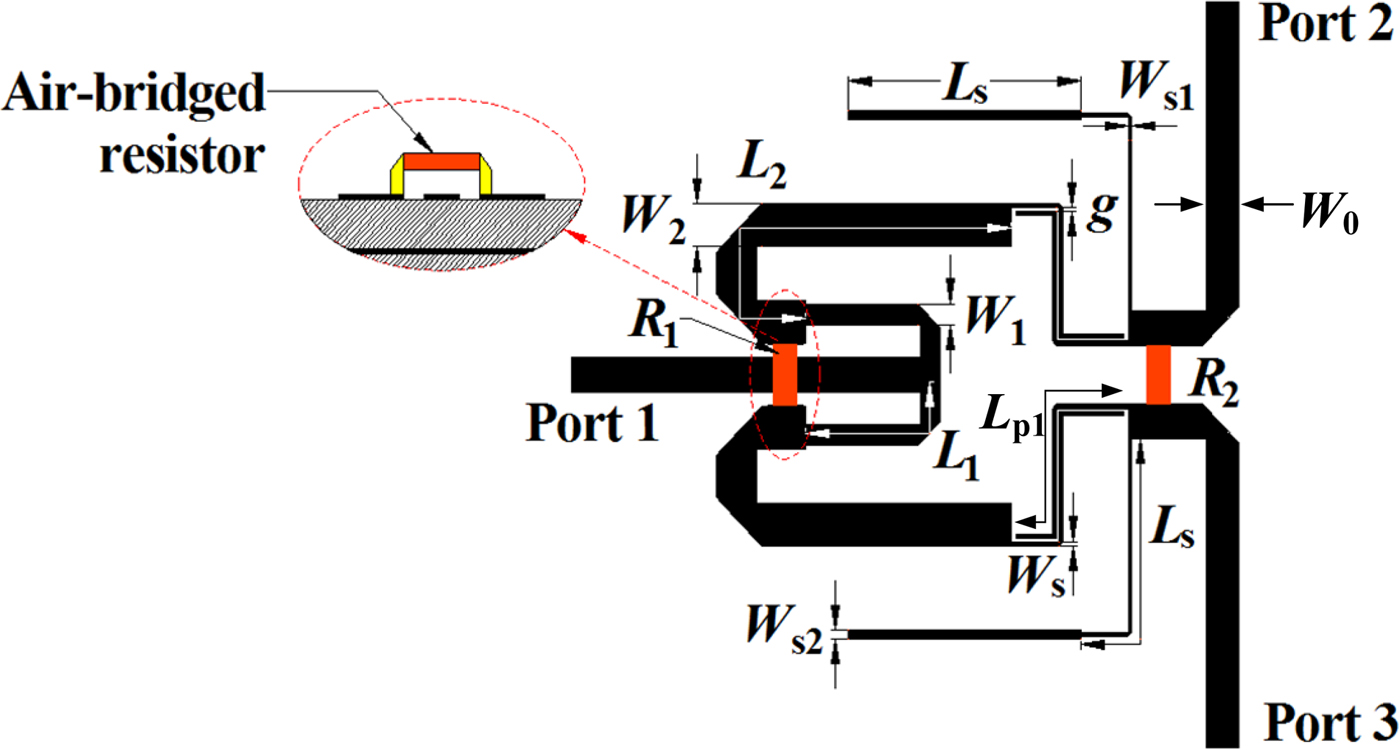
The layout of the proposed power divider is depicted in Fig. 1. The circuit structure can be divided into three parts: impedance converter, filter network, and isolation resistance. Impedance converters are designed in a nested form. The circuit structure is more compact than conventional multi-section impedance converters, achieving similar dimensions as single-node impedance converters. In order to achieve out-of-band rejection of the power divider, the distal impedance converter is replaced by a filter-type network. Parallel coupled lines and parallel open lines are designed to achieve ultra-wideband filtering performance. The end of the coupling line is connected by isolation resistor R 2, thus achieving good isolation and output return loss in the passband.

Fig. 1. Configuration of ultra-wideband power divider.
Since the circuit is symmetrical, the method of analyzing odd and even modes is applied to the design of the ultra-wideband bandpass-response power divider. Figure 2 shows the equivalent circuit model of the presented power divider, and the electrical length of each section satisfies the relationship: θ 1 = θ 2/2 and (θ 1 + θ 2)/2 = θ A = π/2. The equivalent circuit under even-mode excitation is shown in Fig. 3(a), the transfer matrix of [A] is:
 $$\eqalign{& \lsqb A \rsqb = \lsqb A \rsqb _{cl}\lsqb A \rsqb _{st} = \cr & \quad \left[ {\matrix{ {{{a_2} / {Z_o{\rm +} a_1}}} & {a_2} \cr {{{a_2} / {Z_o^2 + {{\lpar {a_1 + a_4} \rpar } / {Z_o + a_3}}}}} & {{{a_2} / {Z_o}} + a_4} \cr}} \right]\left[ {\matrix{ 1 & 0 \cr {{1 / {Z_{st}}}} & 1 \cr}} \right] = \cr & \left[ {\matrix{ {{{a_2} / {Z_o + {{a_2} / {Z_{st} + a_1}}}}} & {a_2} \cr {{{a_2} / {Z_o^2 + {{a_2} / {Z_oZ_{st} + {{\lpar {a_1 + a_4} \rpar } / {Z_o + {{a_4} / {Z_{st} + a_3}}}}}}}}} & {{{a_2} / {Z_o}} + a_4} \cr}} \right],} $$
where a 1, a 2, a 3, Z o, Z st can be expressed as:
 $$a_1 = a_4 = {{\lpar {Z_{ce} + Z_{co}} \rpar \cos \theta _A} / {\lpar {Z_{ce} - Z_{co}} \rpar }},$$
 $$\eqalign{& a_2 = - {\,j / 2}\lsqb {{{4Z_{ce}Z_{co}{\cos}^2\theta_A^{}} / {\lpar {Z_{ce} - Z_{co}} \rpar }}} \cr & \quad {\sin \theta_A - \lpar {Z_{ce} - Z_{co}} \rpar \sin \theta_A} \rsqb ,} $$
 $$a_3 = {{\,j2\sin \theta _A} / {\lpar {Z_{ce} - Z_{co}} \rpar }},$$
 $$Z_o = {2 / {\lpar {{1 / {Z_{ce} + {1 / {Z_{co}}}}}} \rpar }},$$
 $$Z_{st} = {{\,jZ_{s1}(Z_{s1}\tan \theta _{s1} - Z_{s2}\cot \theta _{s1})} / {\lpar {Z_{s1} + Z_{s2}} \rpar }}.$$
The impedances seen from node T are further obtained as:
 $$Z_{in}^{e1} = \displaystyle{{\lpar {{{a_2} / {Z_o + {{a_2} / {Z_{st} + a_1}}}}} \rpar Z_0 + a_2} \over \matrix{\lsqb {{{a_2} / {Z_o^2 + {{a_2} / {Z_oZ_{st} + {{\lpar {a_1 + a_4} \rpar } / {Z_o + {{a_4} / {Z_{st} + a_3}}}}}}}}} \rsqb \hfill \cr \quad Z_0 + {{a_2} / {Z_o}} + a_4 \hfill}}, $$
 $$Z_{in}^{e2} = Z_2\displaystyle{{Z_{in}^e + jZ_2\tan \theta _2} \over {Z_2 + jZ_{in}^e \tan \theta _2}},$$
where  $Z_{in}^e $ can be expressed as
  $Z_{in}^e = Z_1({{2Z_0 + jZ_1\tan \theta _1)} / {(Z_1 + j2Z_0\tan \theta _1)}}$. In order to achieve good matching of the power divider under even-mode excitation, it must be satisfied
  $Z_{in}^{e1} = Z_{in}^{e2 \ast}$. Therefore, the coupling between the odd–even mode impedance of the microstrip line and the impedance of the conversion line can be described by the following formula:
 $$\eqalign{& \displaystyle{{{\displaystyle{{\lpar {Z_{ce} + Z_{co}} \rpar Z_0} \over {Z_{ce}Z_{co}}}} + 2 + \displaystyle{{2Z_0} \over {Z_{st}}}} \over {{\displaystyle{{{\lpar {Z_{ce} + Z_{co}} \rpar }^2Z_0} \over {2Z_{ce}^2 Z_{co}^2}}} + {\displaystyle{{8Z_0} \over {{\lpar {Z_{ce} - Z_{co}} \rpar }^2}}} + {\displaystyle{{(Z_{ce} + Z_{co})} \over {Z_{ce}Z_{co}}}} + \displaystyle{{Z_0(Z_{ce} + Z_{co})} \over {Z_{st}Z_{ce}Z_{co}}}}} \cr & \quad = \left( {\displaystyle{{Z_2\left( {2Z_1Z_0 + j\sqrt 3 Z_1^2 + 6Z_2Z_0 - j\sqrt 3 Z_1Z_2} \right)} \over {Z_2Z_1 + j2\sqrt 3 Z_2Z_0 - j2\sqrt 3 Z_1Z_0 + 3Z_1^2}}} \right)^{^\ast}.} $$
The condition  ${\rm Re} \lpar {Z_{in}^{e1}} \rpar = {\rm Re} \lpar {Z_{in}^{e2 \ast}} \rpar $ can be obtained. When θ s1 is close to π/2 at center frequency,the relationship between Z 1, Z 2, Z ce, and Z co is simplified as
 $$\eqalign{& \displaystyle{{{\displaystyle{{\lpar {Z_{ce} + Z_{co}} \rpar Z_0} \over {Z_{ce}Z_{co}}}} + 2} \over {{\displaystyle{{{\lpar {Z_{ce} + Z_{co}} \rpar }^2Z_0} \over {2Z_{ce}^2 Z_{co}^2}}} + {\displaystyle{{8Z_0} \over {{\lpar {Z_{ce} - Z_{co}} \rpar }^2}}} + {\displaystyle{{(Z_{ce} + Z_{co})} \over {Z_{ce}Z_{co}}}}}} \approx \cr & \quad \displaystyle{{32Z_0Z_1^2 Z_1^2} \over {{\lpar {Z_1Z_2 + 3Z_1^2} \rpar }^2 + 12Z_0{\lpar {Z_1 - Z_2} \rpar }^2}}.} $$
In the odd-mode excitation, the equivalent circuit model is shown in Fig. 3(b). From the impedance matching conditions  $Z_{in}^{o1} = Z_{in}^{o2 \ast}$, it can be deduced that:
 $$\eqalign{& \displaystyle{{{\displaystyle{{\lpar {Z_{ce} + Z_{co}} \rpar Z_0} \over {Z_{ce}Z_{co}}}} + {\displaystyle{{4Z_0} \over {R_2}}} + 2 + {{2Z_0} \over {Z_{st}}}} \over {{\displaystyle{{{\lpar {Z_{ce} + Z_{co}} \rpar }^2Z_0} \over {2Z_{ce}^2 Z_{co}^2}}} + {\displaystyle{{8Z_0} \over {{\lpar {Z_{ce} - Z_{co}} \rpar }^2}}} + {\displaystyle{{2\lpar {Z_{ce} + Z_{co}} \rpar Z_0} \over {Z_{ce}Z_{co}R_2}}} + {\displaystyle{{Z_{ce} + Z_{co}} \over {Z_{ce}Z_{co}}}} + {{Z_0(Z_{ce} + Z_{co})} \over {Z_{st}Z_{ce}Z_{co}}}}} \cr & \quad = \left( {\displaystyle{{Z_2\left( {6Z_1Z_2 + j\sqrt 3 Z_1R_1 - j\sqrt 3 Z_2R_1} \right)} \over {3Z_1R_1 + Z_2R_1 + j2\sqrt 3 Z_1Z_2}}} \right)^{^\ast}.} $$
The condition 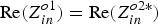 ${\rm Re} \lpar {Z_{in}^{o1}} \rpar = {\rm Re} \lpar {Z_{in}^{o2 \ast}} \rpar $ can be obtained. When θ s1 is close to π/2 at center frequency, the relationship between R 1 and R 2 is simplified as
 $$\eqalign{& \displaystyle{{{\displaystyle{{\lpar {Z_{ce} + Z_{co}} \rpar Z_0} \over \displaystyle{Z_{ce}Z_{co}}}} + {{{4Z_0} \over {R_2}}} + 2} \over {{{{{\lpar {Z_{ce} + Z_{co}} \rpar }^2Z_0} \over \displaystyle{2Z_{ce}^2 Z_{co}^2}}} + {\displaystyle{{8Z_0} \over {{\lpar {Z_{ce} - Z_{co}} \rpar }^2}}} + {\displaystyle{{2\lpar {Z_{ce} + Z_{co}} \rpar Z_0} \over {Z_{ce}Z_{co}R_2}}} + {\displaystyle{{Z_{ce} + Z_{co}} \over {Z_{ce}Z_{co}}}}}} \cr & \quad \approx \displaystyle{{24Z_1^2 Z_2^2 R_1} \over {{\lpar {3Z_1R_1 + Z_2R_1} \rpar }^2 + 12{\lpar {Z_1Z_2} \rpar }^2}}.} $$
In order to achieve ultra-wideband filtering, a sufficiently large coupling coefficient is required. The coupling gap is given as g = 0.1 mm; Z ce = 171 Ω andZ co = 53 Ω are obtained by selecting and optimizing the appropriate coupling line width. Noted that according to (1) and multi-section ultra-wideband Wilkinson power divider circuit theory described in [Reference Sung-Won, Kim, Choi Kwan, Park and Ahn19, Reference Song, Hu, Duan, Chen and Fan21], it is obtained from the calculation: Z 1 = 69 Ω, Z 2 = 42 Ω. According to (10), the relationship between R 1 and R 2 is given by:
 $$\; \displaystyle{{3.27R_2 + 200} \over {0.07R_2 + 2.47}} = \displaystyle{{2015.62R_1} \over {0.62R_1^2 + 1007.81}}.$$
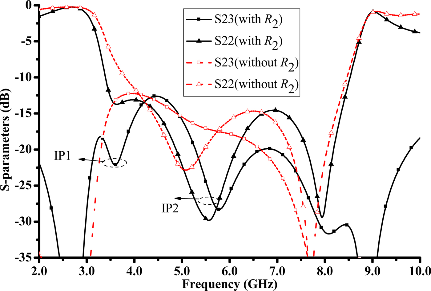
In Fig. 4, the effect of R 2 resistance on output return loss and isolation is demonstrated. When the isolation resistance is loaded at the end of the coupled microstrip line, the isolation curve produces two poles IP1 and IP2 at 3.58 and 5.77 GHz, respectively. At the same time, the output return loss is optimized at similar frequencies. R 2 effectively increases the isolation bandwidth and output return loss.
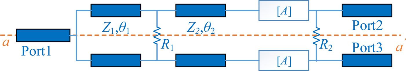
Fig. 2. Equivalent circuit for the proposed power divider.
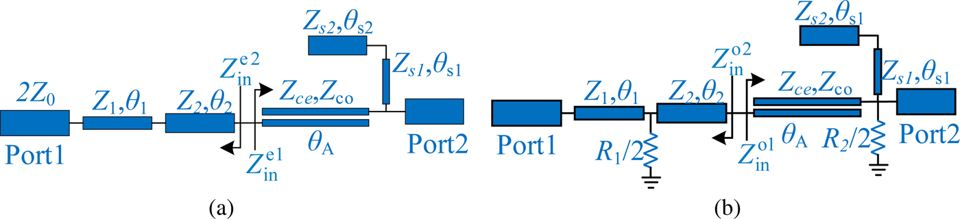
Fig. 3. (a) Even-mode equivalent circuit and (b) odd-mode equivalent circuit.

Fig. 4. Simulated output return loss and isolation for filters with and without R 2.
Based on the structure present in this paper,two transmission zeros (TZ) are generated at lower and upper regions, and the position is determined by the paralleled step impedance line shown in Fig. 1. According to equation (6), when  $Z_{s1}\tan \theta _{s1} = Z_{s2}\cot \theta _{s2}$ is satisfied, transmission zeros are generated at both ends. In order to simplify circuit parameters, always let θ s1 = θ s2. So we can get:
 $$\theta _0 = \theta _{s1} = \theta _{s2} = \arctan \sqrt {R_z}, $$
where R z = Z s1/Z s2. The relationship between lower TZ frequency f 1 and upper TZ frequency f 2 can be expressed as
 $$\displaystyle{{\,f_2} \over {\,f_1}} = \displaystyle{{\theta _2} \over {\theta _1}} = \displaystyle{{\pi - \theta _0} \over {\theta _0}} = \displaystyle{\pi \over {\arctan \sqrt {R_z}}} - 1.$$
According to equations (4)–(6), the position of the TZs at the lower and upper regions can be controlled by adjusting L s, W s1, and W s2 as shown in Fig. 1. Figure 5 shows the position of the lower TZ and the upper TZ with varied L s and W s2. It can be seen that the upper TZ shifts to the high end when the W s2 increases, while the lower TZ is opposite. When adjusting L S, the two transmission zeros move in the same direction. According to such characteristics, the TZ's region can be adjusted appropriately.
Fig. 5. The lower and upper TZ regions varied L s and W s2.
Results and discussion
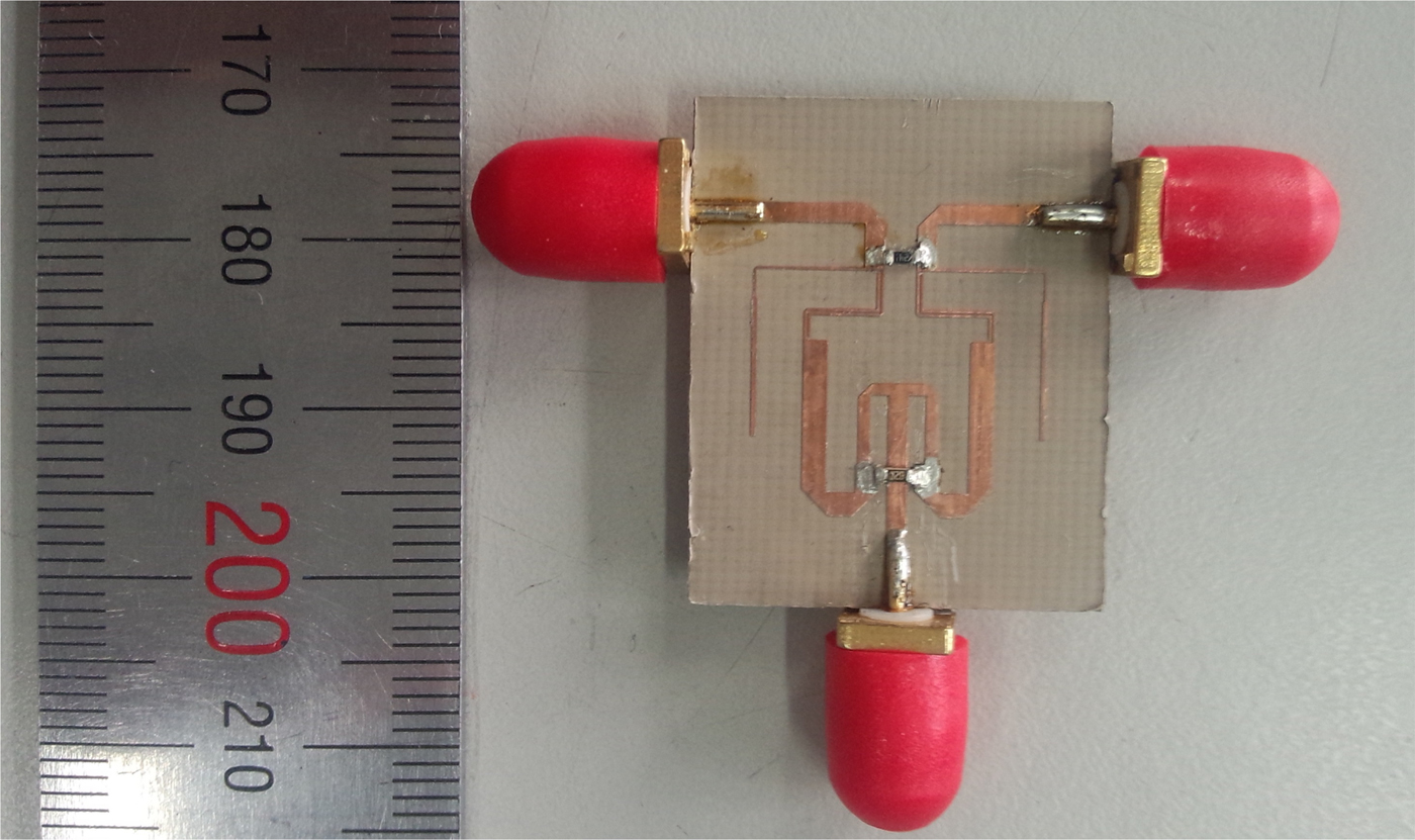
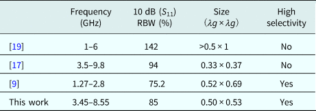
To verify the principle of the above design approach, an ultra-wideband bandpass power divider is designed and optimized by using full-wave simulation software HFSS 15.0. The layout is fabricated on the substrate Taconic RF-35 with a thickness of 0.508 mm and a loss tangent of 0.0018. In the simulation process, air bridge isolation resistance needs to be used, and the height of the solder at both ends is set to 0.6 mm. Through this modeling method, the simulation results are closer to the measured result. After simulation and optimization, the dimensions of the fabricated power divider are chosen as follows: W 0 = 1.15 mm, L 1 = 5.93 mm, L 2 = 14.52 mm, L S = 7.86 mm, W 1 = 0.66 mm, W 2 = 1.38 mm, W s1 = 0.12 mm, W s2 = 0.38 mm, W s = 0.14 mm, g = 0.1 mm, L p = 7.76 mm, R 1 = 82 Ω, R 2 = 240 Ω. The real photograph of the ultra-wideband bandpass-response power divider is shown in Fig. 6. The final circuit size is 15.1 mm × 16 mm (0.50λ g × 0.53λ g), which is the wavelength of the waveguide corresponding to the center frequency. Figure 7 shows the simulation and the measured results of the ultra-wideband bandpass-response power divider. As shown in Fig. 7(a), the designed power divider operates at 3.45–8.55 GHz with a relative bandwidth of 85%. The measured input return loss is better than 11 dB, and insertion loss is better than 1.68 dB in the entire operating band range. Two transmission zeros are generated at 2.8 and 9 GHz and the out-of-band suppression is >13 dB. As shown in Fig. 7(b), output return loss is >13.2 dB in the band. The measured isolation between the output ports is >12.3 dB in the 2.45–8.29 GHz range. As shown in Fig. 7(c), the amplitude imbalance is within ±0.2 dB in the passband. The measured and the simulation results agree well with no frequency offset. The increase of insertion loss, especially in the high-frequency band, is mainly due to the increase of the distribution parameters of the isolation resistance in the high-frequency band. Comparisons between the proposed and the previous ones are listed in Table 1. It can be found that the presented ultra-wideband power divider has the advantages of high-frequency selectivity. At the same time, assembly error of the SMA connector and substrate dielectric loss also increase insertion loss.

Fig. 6. Photograph of the power divider.

Fig. 7. Calculated, simulated, and measured frequency responses of the fabricated power divider: (a) insertion loss and input return loss, (b) output return loss, (c) magnitude imbalance and phase imbalance.
Table 1. Comparisons between the proposed power divider and the reported ones

Conclusion
An ultra-wideband bandpass-response power divider is proposed and validated in this paper. The equivalent circuit of the presented power divider has been developed based on the even–odd mode analysis and has been used to design the presented power divider. The circuit is fabricated and measured. The measured results are in good agreement with the calculated and the simulation results. The power divider is easy to be fabricated and suitable for modern wireless systems.
Acknowledgement
This work was supported by the National Natural Science Foundation of China (Grant No: 61771094) and by the Research Fund of Shanghai Academy of Spaceflight Technology (Grant No: SAST2016094).
 Song Guo was born in Lang Fang, Hebei Province, China, in February 1993. He received the B.Sc. degree in Microelectronics from Harbin Engineering University, Harbin, Heilongjiang, China, in 2006, and is currently working toward the M.Sc. degree in Electromagnetic Fields and Microwave Technology at the University of Electronic Science and Technology of China (UESTC). His research interests include microwave and millimeter-wave power-combining technology and microwave passive component design.
 Kaijun Song (M'09-SM'12) received the M.S. degree in Radio Physics and the Ph.D. degree in Electromagnetic Field and Microwave Technology from the University of Electronic Science and Technology of China (UESTC), Chengdu, China, in 2005 and 2007, respectively. Since 2007, he has been with the EHF Key Laboratory of Science, School of Electronic Engineering, UESTC, where he is currently a Full Professor. From 2007 to 2008, he was a postdoctoral research fellow with the Montana Tech of the University of Montana, Butte, USA, working on microwave/millimeter-wave circuits and microwave remote-sensing technology. From 2008 to 2010, he was a research fellow with the State Key Laboratory of Millimetre Waves of China, Department of Electronic Engineering, City University of Hong Kong, on microwave/millimeter-wave power-combining technology and ultra-wideband (UWB) circuits. He was a senior visiting scholar with the State Key Laboratory of Millimetre Waves of China, Department of Electronic Engineering, City University of Hong Kong in November 2012. He has published more than 80 internationally refereed journal papers. His current research fields include microwave and millimeter-wave/THz power-combining technology; UWB circuits and technologies; microwave/millimeter-wave devices, circuits, and systems; and microwave remote-sensing technologies. Prof. Song is the Reviewer of tens of international journals, including IEEE Transactions and IEEE Letters.
 Yedi Zhou was born in Harbin, Heilongjiang Province, China, in January 1991. He received the B.S. degree from the University of Electronic Science and Technology of China (UESTC), Chengdu, China, in 2013. He is currently pursuing the Ph.D. degree in Electromagnetic Fields and Microwave Technology at UESTC. His research interests include microwave and millimeter-wave power-combining technology.
 Yong Fan (M'05) received the B.E. degree from Nanjing University of Science and Technology, Nanjing, Jiangsu, China, in 1985 and the M.S. degree from the University of Electronic Science and Technology of China, Chengdu, Sichuan, China, in 1992. He is now with the School of Electronic Engineering, University of Electronic Science and Technology of China, where he is currently a Full Professor. His current research interests include electromagnetic theory, millimeter-wave technology, communication, and system. He has authored and co-authored over 130 papers. Mr. Fan is a senior member of the Chinese Institute of Electronics.