


Introduction
The microstrip patch antenna arrays have been adopted widely for a range of multiple input multiple output (MIMO) wireless devices. However, due to the compact nature of wireless devices; the antenna elements in an array have to be closely spaced. This results in the increased mutual coupling between antenna elements, leading to degradation in antenna performance. The size of the antenna plays a crucial role in the design of MIMO antenna arrays for compact wireless devices, as the compact size of the antenna will allow greater spacing between antenna elements compared to conventional antennas. Different types of compact antenna designs, such as design using a dielectric substrate of high permittivity [Reference Fukusako and Nakano1], design with a slot on the patch [Reference Jolani and Dadgarpour2] and design with a destructive ground structure (DGS) or a combination of these have been reported in the literature [Reference Dasari and Karunakar3].
However, miniaturization of microstrip antenna (MSA) causes the resonance bandwidth to shrink to some extent as the quality factor increases during the process. This raises new challenges in compact antenna design, and a tradeoff must exist between the size and bandwidth. A monopole antenna designed with a DGS has been very popular in recent years due to its larger bandwidth and compact size. However, it does not exhibit a stable radiation pattern over its operating frequency. In this paper, a novel compact stack configuration of compact patch elements is proposed. This method utilizes the space in vertical direction available in a device, ensures that the size in the horizontal direction is the same as of the compact patch antenna. Thus, this stack antenna is appropriate to be used as array elements. Isolation between array elements can be enhanced by cutting off the coupling path between the ports of the elements. A majority of researchers have developed different substrate surface wave mitigation techniques. In one of isolation enhancement techniques, DGS is introduced by purposely changing the ground plane of the MGS array [Reference Kamal and Chaudhari4]. However, change of the ground plane may perturb the antenna's radiation pattern and also effect in reduced gain. Isolation between the ports can also be enhanced by mitigating the space waves using metamaterials [Reference Qiu, Peng, Jiang, Sun and Tang5], use of stub loading technique [Reference Liao, Chang, Yeh and Hsiao6], introducing the neutralizing line in array design [Reference Si-yan, Xiao-lin and Zu-fan7] and shorting pins [Reference Singh, Meruva, Pandey, Bharti and Meshram8]. Electromagnetic band gap (EBG) structures in an antenna array provide the isolation between antenna elements for a given band gap [Reference Lee, Kim and Jang9]. To mitigate the mutual coupling through space waves, diversity reception techniques have been applied. The space diversity technique offers the simplest solution. However, the compact nature of wireless devices puts a limitation on the maximum spacing between the antenna elements. Another such technique is polarization diversity where two elements radiate at orthogonal polarizations with respect to each other [Reference Femina and Mishra10].
The main challenge for this work is to discover strategies to simultaneously address the aforementioned issues of compact size, wide bandwidth, and high isolation. The contribution of the authors includes the design of a novel compact stack antenna with compact size and wide bandwidth, design of compact stack EBG structure for enhanced isolation and high bandwidth.
Stack antenna design
The driven and parasitic patch elements of stack antenna are designed with FR4 substrate having dielectric constant (ɛr 1 and ɛr 3 = 4.4), loss tangent 0.02 and height h = h1 = h3 = 1.6 mm. The substrate on which the parasitic patch is etched is placed with an air gap h2 = 5 mm from a driven patch. The air gap acts as a dielectric substrate with dielectric constant ɛr 2 = 1. The driven patch is driven with a coaxial line feed and the electromagnetic coupling with a driven patch excites the top parasitic patch as seen in Fig. 1(a). A shorting pin introduced in the antenna design enhances the coupling between the patches due to the physical connection between the two patch elements and also provides physical rigidness to the antenna, compared to conventional stack design. Both, the driven and parasitic patches are designed with half of the dimension of the conventional patch by introducing a meander line structure as depicted in Fig. 1(b). The driven and parasitic patches are designed with a substrate length (L) = 24 mm and width (W) = 30 mm. While the driven patch is optimized with dimensions of length of patch (lD) = 16.5 mm, width of patch (w) = 22 mm, feed position fixed to (x) = 6.25 mm and short at y = 1.75 mm. Whereas parasitic patch dimensions are optimized to l = 14 mm and width w = 22 mm. The gap S between meander line elements is obtained to be 2.2 mm and width of meander line arm to a = 1 mm for both driven and parasitic patch elements.
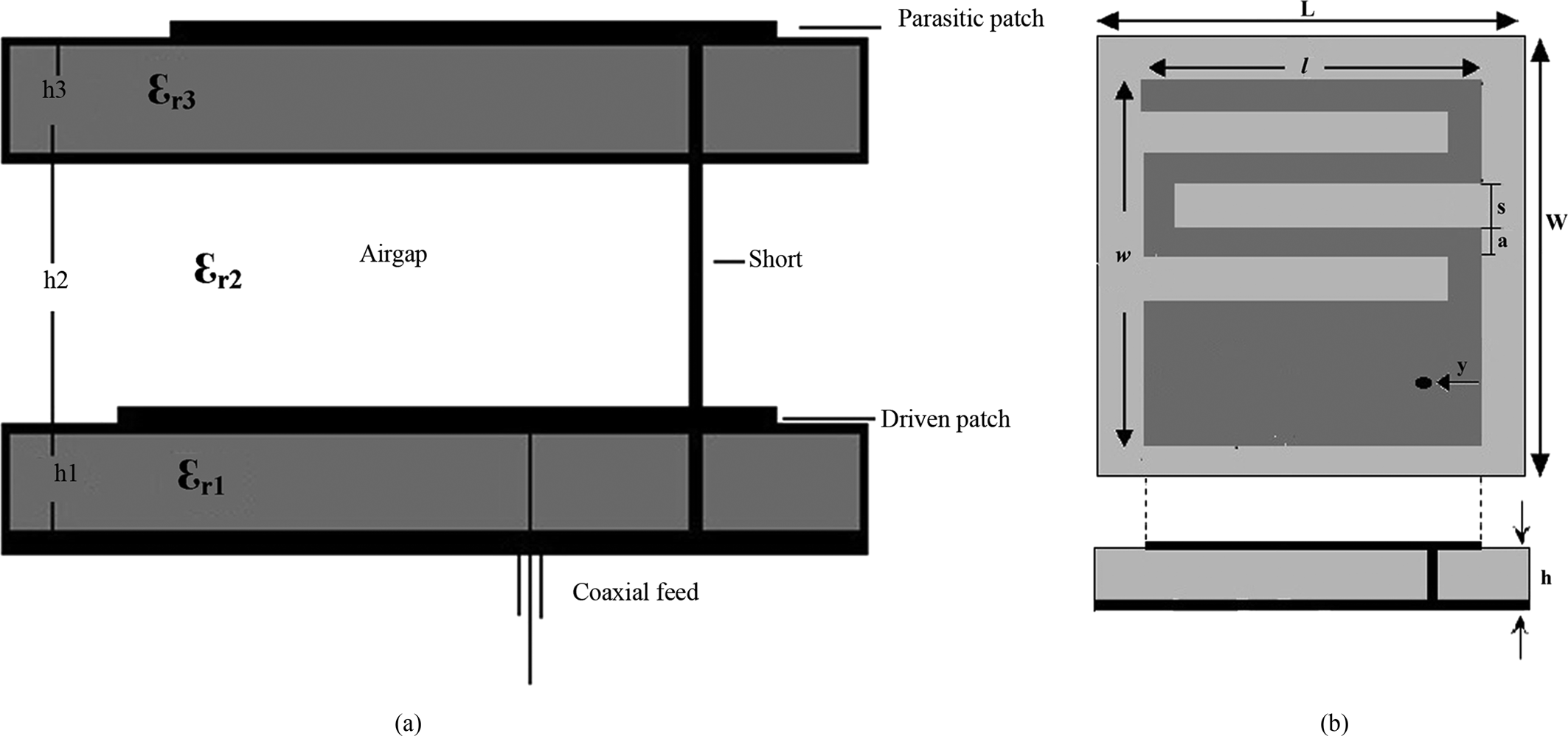
Fig. 1. (a) Side view of stack antenna. (b) Cross sectional view of compact patch.
Thus, tuning of lower resonant frequency with the change in inductance for stack patch antenna is realized by variation of meander line arm length l for the driven patch as demonstrated in Fig. 2(a). Whereas, the tuning of the upper resonant frequency of the stack antenna is dictated by the length l of the meander line arm of the parasitic patch as shown in Fig. 2(b). The combined tuning of resonance of the driven and parasitic patches by variation of length of meander line arm achieves the desired resonance bandwidth for the stacked antenna.

Fig. 2. (a) Lower frequency tuned with meander line arm length of driven patch element. (b) Upper resonant frequency tuned with meander line arm length of parasitic patch element.
Design of high isolation stack antenna array with stack EBG
To mitigate space wave coupling polarization diversity proves to be an effective solution. The two antenna elements of stacked antenna sharing a common substrate are aligned to generate orthogonal polarization to each other. The current distribution in Fig. 3 shows that the electric fields of antenna elements are oriented orthogonal to each other. The antenna 1 orients the field in a vertical direction, whereas for antenna 2 the electric field vectors are in the horizontal direction. Figure 4(b) demonstrates a reduction of 8 dB mutual coupling with the introduction of polarization diversity between driven as well as parasitic elements of the stack antenna.

Fig. 3. Electric field orientation with polarization diversity introduced in array structure.

Fig. 4. (a) Side view of stack EBG structure. (b) Mutual coupling S21 (dB) versus frequency.
Design of compact L slot EBG
The dimensions of the EBG element are a function of its wavelength, which in turn is inversely proportional to the equivalent inductance and capacitance of EBG. Therefore, to provide a realistic solution for a compact EBG design the process for increasing series inductance is realized using the L slot EBG structure [Reference He, Lai, Xu, Jiang, Zang, Ye and Wang11] as shown in Fig. 5(a). The single unit of L slot EBG is designed with a substrate dielectric of FR4 with a relative permittivity of 4.4 and a loss tangent of 0.02. The height of the substrate is 1.6 mm. The corresponding optimized parameters are p1 = 7 mm, p2 = 4.8 mm, and p = 0.8 mm, respectively. Whereas the L slot is constructed with the width u = 0.7 mm.

Fig. 5. (a) Top view of L slot EBG. (b) L slot EBG layer 1.
An L slot EBG layer 1 of 2 × 4 EBG elements arranged as seen in Fig. 5(b) is placed at the center of two array antenna elements with dimensions of We = 12.3 mm and Le = 29.5 mm, the distance between two adjacent EBG element optimized to k = 0.5 mm. The stop band of EBG structure can be determined with a very powerful analysis tool termed as a dispersion diagram. The dispersion diagram is obtained from the inbuilt eigenmode solver feature of Ansoft high-frequency structure simulator (HFSS) software. The simulation utilizes the Brillouin diagram to determine the stop-band of a periodic structure. The advantage is that we can determine the stop band of the entire periodic EBG layer by analyzing a single unit cell. The airbox is used to cover a single unit cell of EBG as shown in Fig. 6(a). It has the same length and width as the EBG unit cell. The height of the airbox is six times the thickness of the substrate material. Then perfect matched layer boundary conditions are defined for the airbox [12]. Finally, the dispersion diagram was computed along the edges of the irreducible Brillouin zone, following the triangle with the points Γ, X, and M [12]. The dispersion diagram of the L slot EBG is depicted in Fig. 6(b) verifies the presence of stop band in proposed L slot EBG.

Fig. 6. (a) Simulation setup for dispersion diagram measurement. (b) Dispersion diagram for L slot EBG.
Design of stack L slot EBG
The isolation bandwidth and amount of isolation offered by the L slot EBG layer 1, discussed in the section above are not enough to match the requirement of a stack antenna array. The limited space available for placement of EBG elements between the patch antennas restricts the increase of both columns and rows of EBG elements in layer 1. This, in turn, puts a limitation on amount and bandwidth of isolation. To overcome this issue a novel stack EBG configuration is proposed in this work. Figure 4(a) demonstrates the proposed three layers of L slot EBG stack structure. EBG layer 1 consists of 2 × 4 elements etched on the same substrate as that of the driven patch antenna, with each of the dimensions as depicted in Fig. 5(b). EBG layer 2 of dimensions same as of layer 1 is etched on the upper substrate between parasitic patch elements. The third EBG layer designed in similarity with layers 1 and 2 is etched on a separate FR4 substrate of dimensions of We = 12.3 mm and Le = 29.5 mm, placed and aligned with EBG layer 1, with an air gap of 0.4 mm between layer1 and substrate of layer 3. A shorting pin connects EBG layers 1 and 3 with the ground element. The coupling between the different layers of EBG results in increasing the overall height H of EBG, leading to an increase in the inductance of EBG (Lebg), which is directly proportional to isolation bandwidth (B.WI) as demonstrated in equations (1) and (2).


The coupling between the three EBG layers provides the desired height. Thus, the novel stack structure widens the bandwidth without increasing the space in the horizontal direction compared to the conventional arrangement of EBG elements. The increase in isolation bandwidth with each EBG layer is demonstrated in Fig. 4(b). The result shows an improvement of 10 dB in mutual coupling with the inclusion of EBG structure in the antenna array.
Results and discussion
Return loss
The photograph of the prototype is shown in Fig. 7(a). For verification of performance, the prototype stack antenna was tested by a 2-port Agilent E5080A network analyzer, while the simulated reflection coefficient (S 11) is obtained from ANSYS HFSS simulation software using a solution data report feature. The simulated and measured reflection coefficients of the proposed stack antenna are shown in Fig. 7(b). It shows that the simulated reflection coefficient is lower than 10 dB in the desired band of operation. The measured resonance band is from 2.37 to 2.54 GHz which is very close to the simulated frequency band. To confirm that the EBG structure in an array does not hamper the individual performance of the stack antenna, the reflection coefficient is measured again for the antenna elements in the array as depicted in Fig. 8(b). Return loss parameters of both antenna elements overlap each other due to the symmetric nature of array design. Although, a little difference in simulated and measured results is observed due to the connector soldering effects.

Fig. 7. (a) Side view of stack antenna. (b) Return loss versus frequency.

Fig. 8. (a) Side view of stack antenna array. (b) Scattering parameters for stack antenna array embedded with L slot EBG structure.
Isolation
The combined effect of polarization diversity and stack L slot EBG structure results in mutual coupling reduction of 18 dB and thus results in enhancement of isolation between ports 1 and 2 of the stack antenna array. For validating these results, a 2 × 1 stack antenna array with stack L slot EBG structure was fabricated as depicted in Fig. 8(a). The scattering parameters of array structure were measured with two port vector network analyzer in an open area test site. The measured and simulated return loss and coupling parameters are plotted in Fig. 8(b). It can be seen that mutual coupling values are well below 29 dB in the desired band, for both the simulated and measured results. A slight variation of the measured result is seen as compared to simulated result. This variation can be accepted within a tolerance value.
MIMO parameters
The proposed array antenna was tested for different MIMO performance parameters such as envelope correlation coefficient (ECC), total active reflection coefficient (TARC), diversity gain (D. G), and mean effective gain (MEG). This section includes the mathematical equations that can be defined as an output variable in HFSS to obtained the MIMO performance parameters.
Envelope correlation coefficient and total active reflection coefficient
Isolation between ports of an antenna array is represented by the ECC value. The acceptable limit of ECC for good quality diversity performance is below 0.5. The ECC value can be calculated from S-parameter values as given in equation (3) below.

where S 11 and S 22 are the return loss values for ports 1 and 2, respectively, while S 21 and S 12 denote the inter port coupling of the array antenna. Both the simulated and measured S parameters are used to compute simulated and measured values of ECC. The value of ECC in the frequency range is well below 0.08 as seen in Fig. 9(a). TARC is derived by combining the effects of both isolation and diversity for a MIMO antenna array. TARC value can be calculated by the S parameters obtained from both simulation and measurement as from equation (4).


Fig. 9. (a) Plot of ECC with frequency. (b) Plot of TARC with frequency.
The average value of TARC derived from simulated and measured S parameters is depicted in Fig. 9(b). The TARC value averaged over different values of θ is well below the acceptable limit of 30 dB.
D. G and MEG
D. G <deleted redundancy text> is the most popular technique defining the diversity performance of MIMO antenna array and its value can be computed by equation (5) given below.

Its maximum value obtained for a practical MIMO antenna array is 10 dB. The proposed antenna array presents the DG value obtained from simulation below 9.98 dB. The measured value is well below 9.96 dB for a given frequency band. MEG is one of the vital parameters for measuring diversity performance in a MIMO system. It is usually defined relative to the isotropic antenna. Mathematically, it is defined as

where i represents the port at which MEG is measured and N represents the number of ports. The desired value of the difference between MEG1, for the port of antenna element 1 and MEG2, derived for the port of antenna element 2 should be within 3 dB for the similar input power at both the ports. The ratio of MEG1/MEG2 is found to be 0.96 by measurement and 0.98 by simulation data of S parameters.

Fig. 10. Anechoic chamber radiation pattern measurement setup.
Radiation pattern
The stack antenna is designed to exhibit a bidirectional radiation pattern as the intended application is a MIMO system that supports a multipath environment and the antenna must be capable of receiving signals in all possible directions. The 2D far-field radiation pattern at 2.45 GHz for single stack antenna without L slot EBG layer is plotted with both simulated and measured values obtained from measurement setup depicted in Fig.10 is shown in Fig. 11. It is plotted with θ variation from 0° to 360° on ϕ = 0° and ϕ = 90° plane and uses the far-field simulation feature of HFSS and anechoic chamber facility for measured results. The stack design yields a bidirectional pattern due to the presence of multiple radiating patches arranged in a stack configuration [Reference Keshari, Kanaujia, Khandelwal, Bakariya and Mehra13, Reference Kumar, Gupta and Gautam14]. Figure 12 depicts the radiation plot of the stack antenna element in a 2 × 1 antenna array in the presence of stack L slot EBG structure. It is found that the stack antenna radiation pattern has a modest variation with the inclusion of the EBG layer in between the two antenna elements. Due to the symmetry property of the stack antenna, the other port exhibits similar radiation patterns.

Fig. 11. Radiation pattern for stack antenna embedded without stack L slot EBG at 2.45 GHz; (a) E plane at ϕ = 0°, (b) H plane at ϕ = 90°.

Fig. 12. Radiation pattern for stack antenna embedded with stack L slot EBG at 2.45 GHz; (a) E plane at ϕ = 0°, (b) H plane at ϕ = 90°.
Comparative analysis
A comparison of the proposed design and previous designs reported in the literature is tabulated in Table 1. It is to be noted that the lowermost frequency band is considered for calculation for free-space wavelength ʎ 0, in the case of the multiband antenna configuration. As seen from the comparison in Table 1, the proposed design offers a high isolation, wide isolation bandwidth and compact array design in the horizontal plane along with flexibility in design, manufactured with the economical substrate and better MIMO performance.
Table 1. Comparison of the proposed design with previous designs

Conclusion
This research work has resulted in the design of a compact high isolation stack antenna array for a MIMO application by incorporating a stack EBG structure. First, a compact stack patch antenna was designed using the FR4 substrate with a dielectric constant of 4.4 resonating at 2.45 GHz frequency band over a wider bandwidth. Later, a stack antenna array embedded with stack L slot EBG structure was designed. The isolation level between two elements of the stack array was enhanced to 18 dB over a bandwidth of 13% by introducing polarization diversity and a wideband stack L slot EBG structure between individual antenna elements. Hence the proposed design is a good candidate for compact wireless devices working in a MIMO environment.
 Mahesh B. Kadu is currently working as an assistant professor in Electronics and Telecommunication Department of Amrutvahini COE, Sangamner, MS, India. He is a Ph.D. research scholar at Symbiosis International (Deemed University), Lavale, Pune, India since 2015.
 Dr. Neela Rayavarapu is currently head of the Electronics and Telecommunication department and a professor in Symbiosis Institute of Technology, Symbiosis International (Deemed University), Lavale, Pune, India. She is a registered Ph.D. guide with Electronics and Telecommunication Department, Symbiosis Institute of Technology, Symbiosis International (Deemed University), Lavale, Pune, India.


