


Introduction
Wireless communication technology is growing very fast and with this advancement requirement of the antenna with different properties also changes simultaneously, which cannot be fulfilled by the conventional antenna. Therefore, the reconfigurability of different properties of antenna as per the requirement with low profile becomes necessary for our current and future miniaturized communication devices. The communication devices are used in fixed places as well as in movable vehicles like cellular radio systems, wireless local area networks, mobile satellite systems etc. The fixed communication devices do not suffer from polarization mismatch loss, so a low profile linearly polarized antenna fulfills the requirement, but movable communication devices face multipath distortion, polarization mismatch loss along with transmitter and receiver orientation constraints. To overcome the above-mentioned problem circularly polarized antenna is required. Therefore, a low profile, compact, polarization reconfigurable antenna removes all the constraints and also very much fulfilling the requirement of advanced communication devices.
Many polarization reconfigurable antennas with different techniques and ideas have been published in the literature. Most of them are based on switching or tuning of electronic devices such as PIN diodes [Reference Lin and Wong1–Reference Nishamol, Sarin, Tony, Aanandan, Mohanan and Vasudevan3], varactor diodes [Reference Lin, Lin, Li and Lee4] or radio frequency (RF) MEMS switches [Reference Lin and Wong5, Reference Kovitz, Rajagopalan and Rahmat-Samii6] for opening or closing some sections of the antenna to change its polarization or resonant frequency [Reference Peroulis, Sarabandi and Katehi7–Reference Hum and Xiong10]. Some of the reconfigurable antennas have used optical devices [Reference Panagamuwa, Chauraya and Vardaxoglou11] or magnetic field tunable ferrites [Reference Pozar and Sanchez12] or substrate with tunable properties like electric field tunable liquid crystals [Reference Liu and Langley13, Reference Zhao, Huang, Qing and Luo14]. Using actuators [Reference Bernhard, Kiely and Washington15–Reference Rajya Lakshmi and Devi20] mechanically reconfigurable antennas have been designed and some of the manually reconfigurable antennas [Reference Tawk, Constantine and Christodoulou21–Reference Zhu, Cheung, Liu and Yuk23] have also been designed in the past. Reconfiguration using electronic devices, optical devices, magnetically tunable ferrites and mechanical actuation is faster in speed but requires external circuits and power supply which made the designed antenna complex, costly, and larger in size, inconvenient for miniaturized communication technology. A manually reconfigurable antenna does not require external circuits or power supply may find applications where low cost, low profile, simple architecture, and quick fabrication is prioritized over switching speed.
This paper presents a manual polarization reconfigurable stacked microstrip patch antenna in which a linearly polarized antenna changes into dual-band circularly polarized when another substrate layer with the same sized square patch stacked on the linearly polarized lower layer antenna and the opposite corner of the top radiating patch is truncated with optimum size along with two slots and a slit. Without the upper layer, the lower square-shaped layer with regular hexagonal radiating patch acts as a linear polarized antenna having a broad impedance bandwidth of 10.56% and a low profile for worldwide interoperability for microwave access (WiMAX) (3.4–3.69 GHz) application band. With the addition of the upper layer, the final structure acts as dual-band circularly polarized antenna and generates impedance bandwidth 12.75% (3.23–3.67 GHz) for (S 11 ≤ −10 dB) with two circularly polarized bands (3.34–3.37 GHz) and (3.66–3.70 GHz) for WiMAX application. So the complete structure comprises of both linearly and circularly polarized antennas with a low profile, compact, low fabrication cost, and reconfigurable property that can be used in our advanced communication devices without any space and polarization constraints and also fulfills the commercial requirement of the smaller antenna with multiple properties and low cost of fabrication.
Antenna design
The proposed stacked microstrip patch antenna has two substrate layers, upper and lower layers with two radiating patches as shown in Figs 1(a) and 1(b). The lower square layer of 36 × 36 × 1.6 mm3 dimension is comprised of a regular hexagonal patch with 12 mm side along with a rectangular perturbation of 12 × 0.6 mm2 size on the radiating patch. The upper square layer of 19 × 19 × 1.6 mm3 dimension is comprised of pair of opposite corner truncated square patch with two slots of 15 × 0.5 mm2 and 5 × 0.8 mm2 dimension and a slit of 5.1 × 1 mm2 size on the radiating patch. The length of two opposite truncated corners of the top radiating patch is 7.1 and 7.2 mm. Lower radiating patch, top radiating patch, and ground plane have been made using thin copper sheet and FR4 material of 1.6 mm height has been used for both lower and upper layers as a dielectric substrate with ɛr = 4.4 and tan δ = 0.02. A probe of 50 Ω impedance with an SubMiniature version A (SMA) connector situated 13.5 mm from the left edge and 14.5 mm from the bottom edge of the substrate has been used to excite the proposed antenna.

Fig. 1. Proposed antenna. (a) Final design and (b) upper layer.
Antenna design procedure with parametric study
During the designing process of the proposed antenna supposed to operate in the WiMAX (3.4–3.69 GHz) application band, many combinations of side lengths of the regular hexagonal radiating patch along with mathematical equations (1) and (2) [Reference Kushwaha and Kumar24] given below have been used to compute the resonant frequency. After parametric calculation with different side lengths, at 12 mm side lengths the primary resonant frequency is 3.84 GHz near to the desired result. Regular hexagonal patch antenna and circular patch antenna are very closely related to each other. Consequently, the resonant frequency of a circular patch antenna (1) along with (2) has been used to calculate the primary resonant frequency of the hexagonal patch antenna

where fr is the resonant frequency of the circular patch antenna; Xmn = 1:8411 for the dominant mode TM11; c is the velocity of light in free space; ɛr is the relative permittivity of the substrate and ae is the effective radius of the circular patch

where s is the side length of the regular hexagonal patch.
After calculating 3.84 GHz as the resonant frequency of the conventional regular hexagonal patch antenna with 12 mm sides, it has been designed and analyzed using simulation software (HFSS ver.13) for finding the impedance bandwidth of the primary resonant frequency. With the co-axial probe position (13.5 mm from the left edge and 14.5 mm from the bottom edge of the substrate) the impedance bandwidth for (S 11 ≤ −10 dB) is 100 MHz (3.65–3.75 GHz) as shown in Figs 2(a) and 2(b). Current distribution on the radiating surface of the antenna at 3.7 GHz frequency is also shown in Fig. 2(c).
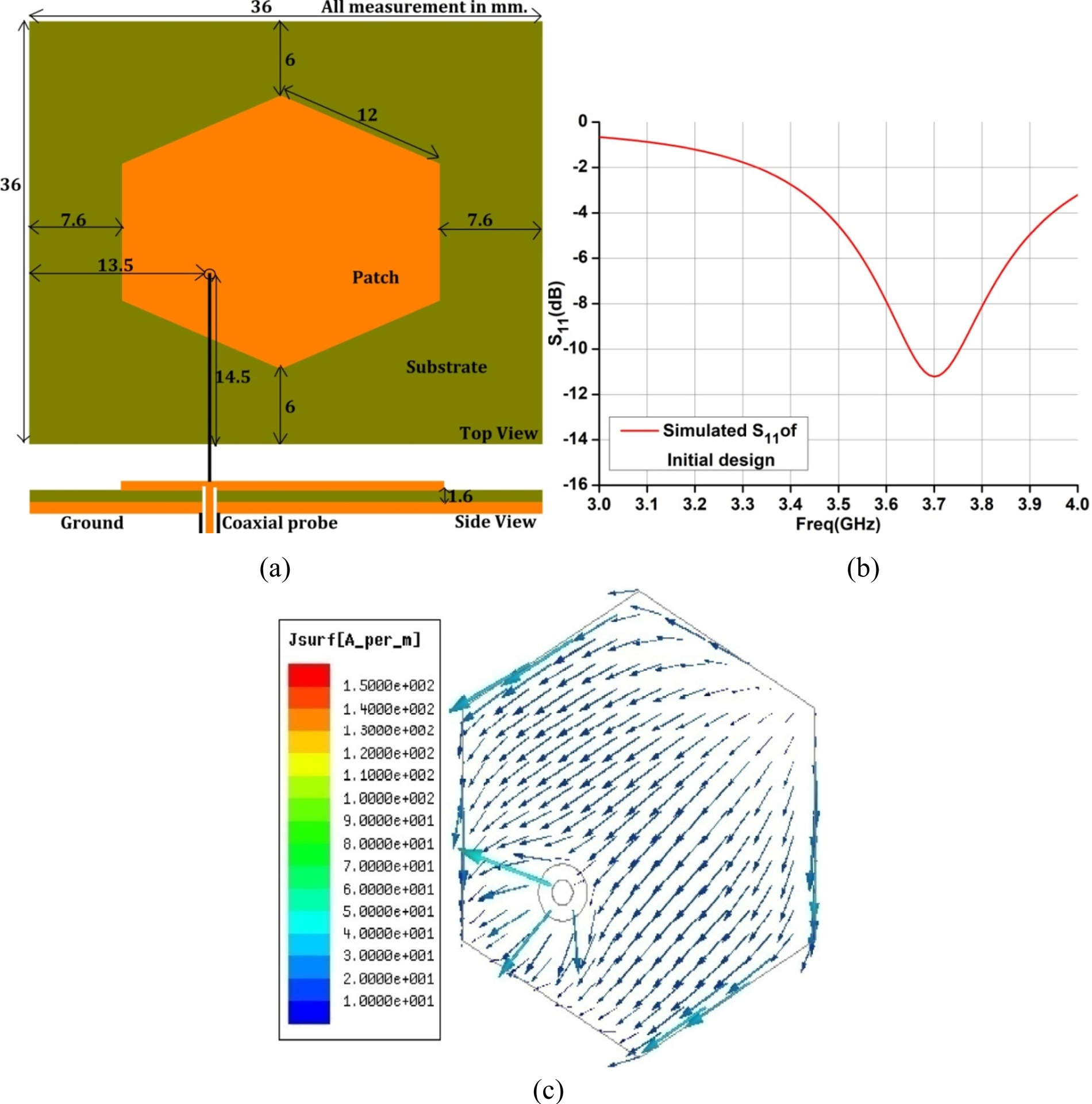
Fig. 2. (a) Initial design of the proposed antenna with probe position 13.5 mm from the left edge and 14.5 mm from the bottom edge of the substrate. (b) S 11 of the antenna at the above-mentioned probe position. (c) Current distribution (simulated) on the radiating surface of the antenna at 3.7 GHz frequency.
The above conventional hexagonal patch antenna is not suitable for any application; therefore, it has been slotted so that it can be used for desired application band.
Effect of slot
The addition of slot on the radiating patch generates higher-order mode because the loading of the patch with the slot causes inclusion of capacitive reactance with it forms a parallel Inductive and capacitive (LC) resonance with stray patch inductances leading to an additional resonant band which when overlaps with the fundamental mode, enhances the overall bandwidth of the antenna and thus the surface current path length increases that causes a shift of resonant frequency towards the lower frequency range [Reference Deshmukh and Ray25–Reference Liu, Gu, Gao and Xu29]. It also decreases the input impedance and causes improvement in impedance matching.
Based on this concept, in order to enhance the bandwidth and lowering of the primary resonant frequency of the conventional antenna so that it can fully cover the desired application band, the patch has been loaded with a rectangular slot. A parametric simulation has been done with 0.6 mm width and various lengths of the slot using high-frequency structure simulator and S 11 and input impedance has been observed. Changes of resonant frequency, bandwidth, and input impedance with different slot lengths are shown in Figs 3(a) and 3(b). With 12 × 0.6 mm2 slot dimension and a distance of 7.7 mm from the top vertex and 1.4 mm from the left side of the hexagonal patch as shown in Figs 3(c)–3(e) the antenna operating band turns out to be (3.32–3.69 GHz) which exactly covers the WiMAX (3.4–3.69 GHz) application band. Also, primary resonant frequency shifted from 3.7 to 3.38 GHz yielding about 8.7% antenna miniaturization. Therefore, this linearly polarized rectangular slotted hexagonal patch antenna with a gain of 2.2 dB at 3.69 GHz can be used for the above-mentioned application band. Current distribution on the radiating surface of the antenna at 3.38 and 3.61 GHz frequencies are also shown in Figs 3(f) and 3(g).
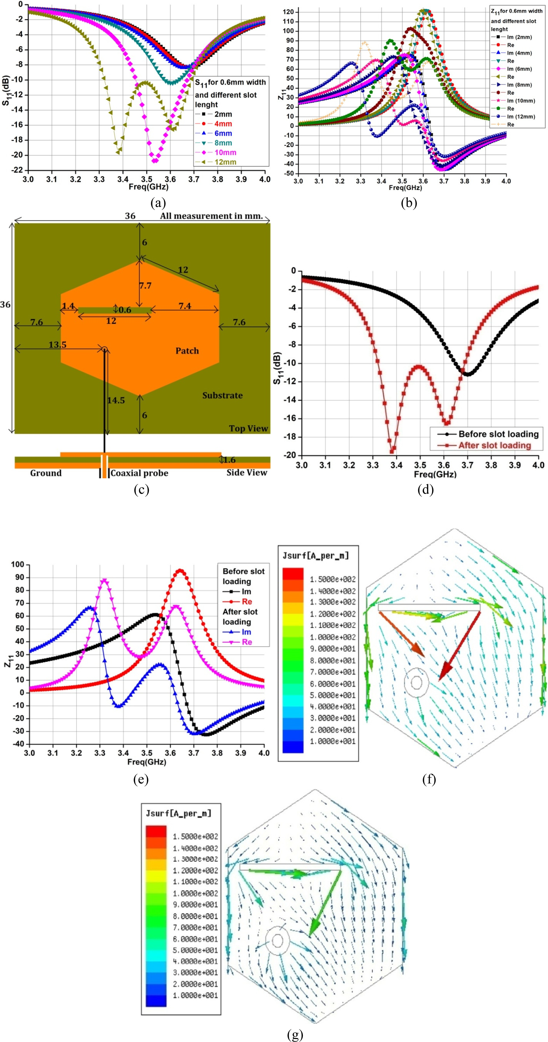
Fig. 3. (a) Changes of the resonant frequency and bandwidth with the change in slot length having constant 0.6 mm width. (b) Changes of the input impedance with the change in slot length having constant 0.6 mm width. (c) Final design of lower layer antenna with the optimized rectangular slot. (d) S 11 before and after the addition of a rectangular slot. (e) Z 11 before and after the addition of a rectangular slot. (f) & (g) Current distribution (simulated) on the radiating surface of the antenna at 3.38 and 3.61 GHz frequencies.
Measured results of the fabricated antenna and software simulated results of the linearly polarized lower layer antenna have been given in Table 1.
Table 1. Software simulated and fabricated measured result of the linearly polarized antenna.

Different measured and simulated parameters of the linearly polarized lower layer antenna are shown in Figs 4–8.

Fig. 4. S 11 (measured and simulated) of the lower layer antenna.

Fig. 5. Radiation pattern (a) E-plane and (b) H-plane at 3.38 GHz frequency.

Fig. 6. Radiation pattern (a) E-plane and (b) H-plane at 3.61 GHz frequency.

Fig. 7. Measured and software simulated input impedance of the antenna.

Fig. 8. (a) Measured and software simulated gain of the antenna. (b) Measured and software simulated radiation efficiency of the antenna. (c) Measured and software simulated realized gain of the antenna. (d) Measured and software simulated antenna efficiency.
Measured and software simulated input impedance of the antenna as shown in Fig. 7.
The gain and S 11 curves seem contradictory, as the gain is still going up at the higher end of the spectrum. The gain plot shown in Fig. 8(a) of the paper is the total gain of the antenna excluding the mismatch effects. On the other hand, the realized gain as shown in Fig. 8(c) contains the mismatch losses. It can be seen from Fig. 8(c) that the realized gain has appreciable magnitude only inside the operating band (3.32–3.69 GHz) of the structure. Outside the operating band when the return loss (S 11) increases, the realized gain reduces, as expected.
An explanation for the monotonically increasing radiation efficiency is similar to the gain case above. Radiation efficiency is defined as the ratio of power radiated to the power accepted by the antenna. It does not include the mismatch losses. On the other hand, the antenna efficiency includes the mismatch losses at the antenna input terminal and is consequently defined as the ratio of the power radiated to the total power incident on the antenna. As can be seen from Fig. 8(d), the antenna efficiency for the proposed antenna follows the intuitively understandable behavior of almost constant in the operating band (3.32–3.69 GHz) and reducing outside the operating band.
Radiation pattern shows the radiation characteristics of the antenna as a function of space coordinate. The performance of linearly polarized antennas is often described in terms of E and H-planes. The E and H-planes are defined as the radiating planes containing the electric field vector (co-pol and x-pol) and the magnetic field vector (co-pol and x-pol). Figures 5 and 6 show the software simulated and fabricated measured co-pol and x-pol in two-dimensional E and H-planes at 3.38 and 3.61 GHz frequencies with Φ = 0° and 90° and theta (θ) between 0° and 360°. It can be seen from Figs 5 and 6 that the proposed antenna has broadside radiation pattern with co-pol and x-pol 12.5 and 11.3 dB at 3.38 and 3.61 GHz frequencies which is in the acceptable range.
Equivalent circuit modal
To provide an enhanced insight and physical analysis into the designed antenna, an equivalent circuit model representing the functioning of the antenna has been shown in Figs 9 and 10. The circuit model has been developed by fitting the simulation S-parameters into the prototype circuits and using ADS Software. The equivalent circuit is basically a higher-order multi-pole circuit with multiple inductors and capacitors. The circuit is made under the assumption that a higher-order circuit model is required to model the frequency sensitive and high Q nature of the S-parameter of the original circuit. Consequently, the prototype circuit is not a physical model but rather an empirical one imitating the original circuit terminal behavior.

Fig. 9. (a) Equivalent circuit model of lower layer antenna. (b) Comparison of S 11 of equivalent circuit model with S 11 of HFSS.

Fig. 10. (a) Equivalent circuit model of final proposed antenna. (b) Comparison of S 11 of equivalent circuit model with S 11 of HFSS.
The linearly polarized patch antenna suffering from multipath distortion and polarization mismatch loss requires the circularly polarized antenna to overcome these problems. Therefore, in order to convert the above-designed antenna into the circularly polarized antenna and also to further improve the performance, another square-shaped substrate layer along with the same shape and size radiating patch has been placed on the lower substrate layer and the upper radiating patch soldered with the coaxial probe. After that, the opposite corner of the top radiating patch is truncated and the two slots and a slit are also introduced.
Effect of addition of upper substrate layer and corner truncation
The addition of upper layer decreases the input impedance of the overall structure causing improvement in impedance matching and lengthening of the surface current path that causes a shift of resonant frequency towards the lower frequency range, which can be seen in Figs 11(a) and 11(b). The size of the upper substrate along with patch has been optimized by varying the size of it and observing the corresponding results of S 11 and input impedance. The optimum size has been found to be 19 × 19 mm2 and increasing it beyond this gives undesired results.

Fig. 11. (a) S 11 of the designed antenna before and after the addition of the upper layer. (b) Input impedance before and after the addition of the upper layer. (c) Changes of axial ratio with different corner truncation area. (d, e, f, and g) Current distribution (simulated) on the surface at 3.35 GHz frequency for different time instants. (h) Design of the antenna after the addition of the upper layer and corner truncation. (i) S 11 after the addition of the upper layer and corner truncation.
Next, in order to change the polarization of the overall structure from linear to circular, the opposite corner of the top square radiating patch has been truncated. The opposite corner truncation generates two near degenerate modes with 90° out of phase [Reference Kumar, Viswakarma, Kumar, Anguera and Andujara30–Reference Saraswat, Kumar and Harish32] and also alters the surface current distribution leading to the generation of the circularly polarized wave. The truncation amount of the corner controls the relative phase of the degenerate modes. Based on this concept, a parametric simulation on the corner truncation amount has been done using the simulator software and the axial ratio has been observed. Changes of the axial ratio with the amount of corner truncation and the current distribution on the surface at 3.35 GHz frequency for different time instants are shown in Figs 11(c)–11(g).
In this way, a linearly polarized antenna becomes circularly polarized with circularly polarized bandwidth 0.9% (3.34–3.37 GHz) for (axial ratio ≤ 3 dB) and impedance bandwidth for (S 11 ≤ −10 dB) is 300 MHz 8.85% (3.24–3.54 GHz) as shown in Figs 11(h) and 11(i).
Effect of first slot on the top radiating patch
In order to enhance the bandwidth of the above circularly polarized antenna so that it can cover more application bands, the top patch has been loaded with a rectangular slot. The size and position of the slot have been optimized by varying the size and position on the radiating patch and observing the corresponding results. With 15 × 0.5 mm2 slot dimension and position as shown in Fig. 1, the stacked antenna operating band turns out to be (3.23–3.74 GHz). Therefore, impedance bandwidth for (S 11 ≤ − 10 dB) becomes 510 MHz 14.63% and enhanced by 5.8% with the generation of another circularly polarized band (3.66–3.70 GHz) for (axial ratio≤3 dB) as shown in Figs 12(a)–12(c) due to reason mentioned in (section ‘Effect of a slot’).

Fig. 12. (a) Design of the stacked antenna after first slot on the top radiating patch. (b) S 11 of the stacked antenna after first slot on the top radiating patch. (c) The axial ratio of the stacked antenna after first slot on the top radiating patch.
Effect of second slot and slit on the top radiating patch
It can be observed from Fig. 12(b), some portion of (3.23–3.74 GHz) frequency band has a return loss of more than (−10 dB) due to high input impedance leading to poor impedance matching.
Perturbation of the top radiating patch with optimized slit and second slot as shown in Fig. 1 decreases the input impedance between the said bandwidth. Therefore, the input impedance shifted near 50 Ω value, as shown in Figs 13(a) and 13(b) and the satisfactory impedance matching and axial ratio (S 11) are obtained in the bandwidth.

Fig. 13. (a) S 11 and (b) Input impedance of the antenna after perturbation with first slot, second slot and slit on the top patch of the upper layer.
These are the above-mentioned procedures which have been used to design the final structure of the antenna. A prototype of the final structure has been fabricated as shown in Figs 14(a)–14(d) and different parameters of the antenna have been measured using VNA bench top (Model No.E5071B) and anechoic chamber.

Fig. 14. Photograph of fabricated prototype antenna. (a) Top view of the lower layer. (b) Bottom view of lower layer. (c) Top view of upper layer. (d) Top view of the complete stacked antenna.
Results
The software simulated and fabricated measured result of the final circularly polarized antenna has been given in Table 2.
Table 2. Simulated and measured result of the circularly polarized antenna.

A very good resemblance has been seen between the software simulated and fabricated measured results of the return loss, axial ratio, input impedance, radiation pattern, and gain of the prototype antenna as shown in Figs 15–19. However, a very small shift can be observed in the measured results because of improper connector soldering, absence of ideal measuring environment [Reference Xu, Xu, Liu, Li and Liu33], and inhomogeneous dielectric constant of the substrate [Reference Zhang, Gong, Li and Wang34], which is not considered at the time of the simulation. The performance of the circularly polarized antennas is often described in terms of E-plane (X–Z) and H-plane (Y–Z). The E- and H-planes are defined as the radiating planes containing the electric field vector (RHCP and LHCP) and the magnetic field vector (RHCP and LHCP). Figures 16(a)–16(d) show the simulated and measured RHCP and LHCP in two-dimensional E and H-planes at 3.36 and 3.6 GHz frequencies with Φ = 0° and 90° and theta (θ) between 0° and 360°. It can be seen from Figs 16(a)–16(d) that the proposed antenna has good difference between RHCP and LHCP in both E-plane and H-plane.

Fig. 15. Software simulated and fabricated measured S 11 of the antenna.

Fig. 16. (a and b) Radiation pattern (Normalized) X–Z and Y–Z planes at 3.36 GHz. (c and d) Radiation pattern (Normalized) X–Z and Y–Z planes at 3.6 GHz.

Fig. 17. Measured and simulated gain of the antenna.

Fig. 18. Axial ratio of the antenna.

Fig. 19. (a) Measured and simulated input impedance of the antenna. (b) Measured and simulated radiation efficiency of the antenna.
The gain of the proposed antenna is little low because the substrate used in the antenna is FR4 which is the lossy substrate. Therefore, it is one of the reasons for low gain of the antenna. Another reason is that, a constant (input excitation) amount of power is distributed to all operating bands of the antenna. Achievement of a circularly polarized radiation necessitated the excitation of two closely spaced orthogonal modes in the designed antenna. Consequently, input power is distributed between these two modes and subsequent interaction between the radiated far-fields from these two modes lead to an eventual reduction in the overall gain of the antenna.
Equivalent circuit modal
A performance comparison of the proposed work with previously reported work, those available in the literature is presented in Table 3, shows the merit of the proposed antenna.
Table 3. Comparison of proposed antenna performance with existing cases in literature.

Where λ 0 is the free space wavelength.
Conclusion
A stacked microstrip patch antenna having two square substrate layers and two radiating patches with polarization reconfigurable property has been designed for the WiMAX application. Lower square substrate layer having regular hexagonal radiating patch acts as a linear polarized antenna with impedance bandwidth of 10.56% (3.32–3.69 GHz) cover WiMAX (3.4–3.69 GHz) application band. Also, the theoretical calculation has been done with various combinations of side lengths of the regular hexagonal patch and mathematical equation to find the desired resonant frequency of the conventional hexagonal microstrip patch antenna. The hexagonal radiating patch perturbed with an optimum rectangular slot to enhance the impedance bandwidth. After the lower layer stacked with the upper layer and opposite corner of the top radiating patch truncated, then the antenna becomes circularly polarized. The top radiating patch also perturbed with two slots and a slit in order to generate another resonant band along with improvement in impedance matching and S 11. Therefore, the stacked antenna generates two circularly polarized resonant bands with impedance bandwidth of 12.75% (3.23–3.67 GHz) for WiMAX application. Equivalent circuit model for both linearly polarized and circularly polarized antenna also given for better insight of the proposed antenna. Therefore, the complete structure has both linearly and circularly polarized antennas with a low profile, compact, low cost, and reconfigurable property suitable for advanced miniaturized communication devices without any space and polarization constraints and also as per the demand of commercial requirement of the smaller antenna with multiple properties and low cost of fabrication.
Acknowledgement
The authors thank Professor (Dr.) Bhaskar Gupta and Joydeep Paul research scholar of Jadavpur University for allowing them to use the HFSS ver.13 software in his lab as well as the measurement of different parameters of fabricated antenna.
 Murari Shaw was born on July 4, 1980. He received his M.Tech. from Calcutta University in 2015. His research interests include Microstrip Patch antenna.
 Niranjan Mandal was born in 1953. He received his B.Tech (Hons.) from IIT, Kharagpur, M.Tech from IIT, Delhi and Ph.D. fro BITS, Rajasthan.
 Malay Gangopadhyay was born in 1979. He received his M.Tech. from Calcutta University and Ph.D. from Jadavpur University. His research interests include Microstrip Patch antenna.


