


Introduction
Composite right/left handed transmission lines (CRLH TLs) acknowledged by split ring resonators (SRRs) are turning into an intriguing and promising subject of research as far back as early 2000 [Reference Smith, Padilla, Vier, Nemat-Nasser and Schultz1, Reference Lai, Caloz and Itoh2]. In order to accomplish the fundamental requirements of wireless devices such as high compactness, low manufacturing cost, low loss, and high selectivity, different structures of diplexer have been acquainted. In the advancement of the modern communication framework, today the scaling down of the microwave diplexers and enhancing the performance parameters turns out to be more critical and tough challenge [Reference Yan, Zhou and Cao4–Reference Shao and Chen11]. The wireless communication system with the blend of WiMAX (IEEE 802.16 standard, operating at 3.3–3.9 GHz with a bandwidth of 600 MHz) and WLAN (IEEE 802.11 standard operating at 5.15–5.85 GHz with a bandwidth of 700 MHz) are in mainstream these days [Reference Zayniyev and Budimir3].
The diplexer [Reference Yan, Zhou and Cao4] based on half and quarter wavelength resonators shows a good isolation of >30 dB but has relatively poor insertion loss at the passbands (2.2 dB at 1.82 GHz and 2.1 dB at 2.41 GHz). It avoids the use of T-section yet compactness is still the problem. Ref. [Reference Chen, Zhu, Bu and Cheng5] uses a dual-mode resonator as the common resonator to integrate two bandpass filters (BPFs). This diplexer does not include metal via but the involvement of backside slots increases the fabrication cost and design complexity. Isolation of >40 dB is obtained in the diplexer reported in [Reference Chen, Yu and Sun6], which uses stub loaded parallel coupled lines, however it occupies a large volume of 45 × 36 mm2. In [Reference Bukuru, Song and Xue7], resonators with dual rectangular spirals are used to design the diplexer. Although size of the diplexer is relatively small of 21.8 × 5.79 mm2 and has wide upper stopband characteristic, but fractional bandwidth (FBW) is low (11.26% at 3.65 GHz and 10.8% at 5.2 GHz) and poor isolation of >25 dB as compared with the work presented in this paper. For a low insertion loss, the diplexer [Reference Rezaei, Noori and Mohammadi8] is designed using coupled lines and spiral cell, however by compromising with low isolation between the two channels of >22.7 dB. The CRLH TL-based diplexer reported in [Reference Rezaei, Noori and Mohammadi8, Reference Li, Xu, Ai and Liu9] uses metal via holes to ground and have relatively large size of 31.4 × 8.8 mm2 [Reference Li, Xu, Ai and Liu9] and 54.48 × 44.15 mm2 [Reference Zeng, Wang, Wei and Wang10]. Although the diplexer presented in [Reference Shao and Chen11] has a good isolation of >35 dB, but suffers from relatively large size of 43.4 × 23.5 mm2 and having greater fabrication complexity because of the use of number of vias on the resonators and matching network.
This paper presents the design of a compact planar via-free CRLH TL-based diplexer for the WiMAX and WLAN applications. Outline idea associated with this is taking the utilization of MSRR having right-angled corners and incorporates meander paths. Exceptionally basic outline thoughts are considered by joining the two BPFs designed by MSRR, working at different frequencies with conventional T-section, which results in good isolation (>32.5 dB) between the two channels and improved upper stopband attenuation. Lumped circuit model results and the simulated results for the planar CRLH diplexer are obtained from commercially available ADS software, using circuit simulator and momentum simulator of ADS respectively and measurements were performed by a vector network analyzer.
Analysis and design of RAC-MSRR unit-cell
The outline design of the proposed right-angled corner-modified split ring resonator (RAC-MSRR) unit-cell is delineated in Fig. 1. Outer ring with length L OR = (L 9 + L 7 + nL 1 + L 3 + L 8) and inner ring with length L IR = (L 10 + L 6 + nL 2 + L 4 + L 5) are alternately connected to the TL section running parallel and maintaining a gap of 0.1 mm. Here n indicates number of meander path formed by outer ring meander path length L 1 and inner ring meander path length L 2. In Fig. 1, unit-cell is having n = 2 meander paths. By changing path length L 1 and path length L 2, shift in resonant frequency is observed which is shown in Fig. 2(a). For getting the effect of number of meander path n in the resonant frequency, all the dimensions for unit-cell were taken into consideration from Table 1 of BPF1. It is found that with increasing number of meander path n, the resonant frequency shifted toward lower resonant frequency. Resonant frequency is 5.06 GHz for n = 2 and it decreases to 2.65 GHz for n = 6. Basically by adding meander paths, total length of the inner ring L IR and outer ring L OR is increased keeping area unchanged and hence size reduction is achieved. The center frequency can be easily tuned by varying the meander path length of the RAC-MSRR. Implementation of RAC-MSRR unit-cell satisfies the case of non-resonant approach for designing of left handed (LH) TL as average unit-cell size, p = (2L 12 + L 11) ≪ λ g where, λ g is the guided wavelength at f 1.

Fig. 1. The geometric configuration of CRLH TL based proposed RAC-MSRR unit-cell.

Fig. 2. (a) Effect of number of meander path “n” in the resonant frequency. (b) Dispersion curve showing variation of LH and RH regions with the number of meander path “n”.
Table 1. Comparison of proposed CRLH TL unit-cell with other reported CRLH TL unit-cell.

a 50 Ω input and output feed lines are not considered.
From the dispersion curve of proposed RAC-MSRR unit-cell shown in Fig. 2(b), it is observed that for n = 2, LH propagation region is 4.11 GHz < f LH < 4.76 GHz and right-handed (RH) propagation region is 5.59 GHz < f RH < 6.56 GHz. For n = 4, LH propagation region is 2.7 GHz < f LH < 3.25 GHz and RH propagation region is 3.82 GHz < f RH < 5.04 GHz and for n = 6 LH and RH region are 2.09 GHz < f LH < 2.37 GHz and 2.82 GHz < f RH < 3.84 GHz, respectively.
The equivalent lumped circuit model shown in Fig. 3 demonstrates the profound knowledge to comprehend the behavior of the proposed RAC-MSRR unit-cell geometry (shown in Fig. 1). Lumped elements L R (nH) and C R (pF) in the equivalent circuit model represent the TL section which adds RH TL characteristic. L L (nH) and C L (pF) are generated due to the inner and outer rings and the gap between them, showing the LH TL characteristics. The lumped parameters of the circuit model are calculated using the pseudo-inverse matrix technique [Reference Kou, Shi and Li14]. Characteristic impedance Z c(ω) for the equivalent symmetrical T-circuit model of unit-cell can be written as
 $$Z_c(\omega ) = \sqrt {Z(\omega )[Z(\omega ) \times (2/Y(\omega ))]} $$
where Z(ω) and Y(ω) are the series impedance and shunt admittance respectively. Z(ω) and Y(ω) are given as
 $$Z(\omega ) = j(\omega L_R-1/\omega C_L)$$
 $$Y(\omega ) = j(\omega C_R-1/\omega L_L)$$
Fig. 3. Equivalent circuit model of proposed RAC-MSRR unit-cell.
For the symmetrical T-network, ABCD parameters are given as
 $$\left[ {\matrix{ A & B \cr C & D \cr}} \right] = \left[ {\matrix{ {1 + ZY/2} & {Z(1 + ZY/4)} \cr Y & {1 + ZY/4} \cr}} \right]$$
Here Z(ω) and Y(ω) are represented as Z and Y respectively, for simplicity. Using equation (4), Z and Y can be interpreted as
 $$Z = 2(A-1)/C;\quad \; Y = C$$
For N distinct frequency points Z and Y in matrix form can be written as
 $$\lsqb Z \rsqb = \lsqb \omega \rsqb \left[ {\matrix{ {L_R} \cr {1/C_L} \cr}} \right];\quad \; \lsqb Y \rsqb = \lsqb \omega \rsqb \left[ {\matrix{ {C_R} \cr {1/L_L} \cr}} \right]$$
where
 $$\lsqb \omega \rsqb = \left[ {\matrix{ {\matrix{ {\,j\omega_1} & {-1/\omega_1} \cr {\,j\omega_2} & {-1/\omega_2} \cr}} \cr {\matrix{ \vdots & \vdots \cr {\,j\omega_N} & {-1/\omega_N} \cr}} \cr}} \right]$$
Lumped circuit parameters L R, C R, L L, and C L is then calculated by solving
 $$\left[ {\matrix{ {L_R} \cr {1/C_L} \cr}} \right] = \lsqb {\omega^{^\ast}} \rsqb \lsqb Z \rsqb ;\quad \; \left[ {\matrix{ {C_R} \cr {1/L_L} \cr}} \right] = \lsqb {\omega^{^\ast}} \rsqb \lsqb Y \rsqb $$
where [ω*] represents the pseudo-inverse matrix of the [ω] matrix.
Table 1 shows the comparison of the proposed CRLH TL unit cell with other reported CRLH TL unit cell. From the table it can be inferred that the proposed CRLH TL unit cell geometry is comparably smaller in size and provides the ease in fabrication either in terms of involvement of via to ground or the use of any metal patterns at the ground which require extra processing steps for development.
Design and analysis of BPF1 and BPF2
BPF1 and BPF2 are designed by cascading two RAC-MSRR unit-cells as shown in Fig. 4. Here, n = 2 and n = 4 are chosen in order to obtain the working center frequency of f 1 and f 2, respectively, for BPF1 and BPF2. The proposed BPFs are designed on FR4 substrate with relative dielectric constant, ε r = 4.4, substrate thickness of 0.8 mm and loss tangent, tan δ = 0.02. To obtain the desired passband characteristics, physical dimensions of both the filters are optimized by using electromagnetic simulator ADS. The final dimensions of the proposed BPF1 and BPF2 are listed in Table 2.

Fig. 4. Layout of the proposed BPFs with two cascaded RAC-MSRR unit-cell (a) BPF1 and (b) BPF2.
Table 2. Dimensions of BPF1 and BPF2 (all units are in mm).

The parameters of the equivalent lumped LC circuit of BPF1 and BPF2 are calculated using the methods mentioned in section “Analysis and design of RAC-MSRR unit-cell” and are tabulated in Table 3.
Table 3. Component values of equivalent lumped LC circuit model for BPF1 and BPF2.

The dispersion characteristics (ω − β plot) for the BPF1 and BPF2 are depicted in Fig. 5. It can be seen from the plot that for BPF1, LH propagation region is 3.01 GHz < f LH < 3.28 GHz and RH propagation region is 3.78 GHz < f RH < 4.09 GHz and for BPF2, LH propagation region is 4.72 GHz < f LH < 5.2 GHz and RH propagation region is 5.82 GHz < f RH < 6.27 GHz.

Fig. 5. Comparative simulated and equivalent circuit model dispersion curve for BPF1 and BPF2.
The comparative S-parameters versus frequency responses for electromagnetic (EM) simulation and equivalent circuits are shown in Fig. 6. However, some discrepancy is there which are due to the limitations involved with pseudo-inverse matrix as it gives only the approximate solution.

Fig. 6. Comparative simulated and equivalent circuit model S-parameter versus frequency plot for (a) BPF1 and (b) BPF2.
For BPF1, simulated −3 dB passband frequency range is 3.17–3.89 GHz with FBW of 20.5% and for BPF2 it is 5.02–5.98 GHz with FBW of 17.4%. At the center frequencies of BPF1 and BPF2, simulated insertion loss |S 21| is −0.59 dB with return loss |S 11| is −19 dB for BPF1 and for BPF2, simulated insertion loss |S 21| is −0.78 dB with return loss |S 11| is −17.31 dB. More than 20 dB rejection level is obtained for wide upper stopband frequency, 4.37–7.97 GHz for BPF1 and 6.65–10.21 GHz for BPF2. Reasonable similarity can be seen between the EM simulation and circuit model responses which validates the design process for both the filters.
Proposed diplexer prototype design
After streamlining and getting the required responses of the two BPFs utilizing RAC-MSRR as the essential building unit, diplexer is designed. The configuration of the proposed diplexer prototype is depicted in Fig. 7. The proposed diplexer is designed by BPF1 and BPF2, where both BPFs are differing just by their physical dimensional parameters to provide the two desired distinct passbands. BPF1 and BPF2 are connected by a T-section at the input side. The length of the T-section line is much shorter than the guided wavelength of the structure at frequency f 1 or f 2 and as a result it shows negligible distributed effect. Dimensions of the T-section line connecting two BPFs and the input port for the diplexer are as follows: D 1 = 2.5 mm, D 2 = 1.5 mm, D 3 = 7.3 mm, and D 4 = 1.2 mm. At f 1, the waves emerging from the input port1, for the most part guided to BPF1 and hence to the output port2. Here, the BPF2 channel is viewed as open circuit at the frequency of f 1. While at f 2, BPF1 is viewed as open circuit and the waves are mostly guided to BPF2.

Fig. 7. Geometric structure of the proposed diplexer.
In order to have deep insight to comprehend the behavior of the proposed diplexer geometry (shown in Fig. 7), the equivalent circuit model is presented in Fig. 8. The equivalent circuit model of the diplexer is formed of equivalent lumped circuits for BPFs and a T-section. All the parameter values for the circuit shown in Fig. 8 are taken the same as that of the individual BPF which are tabulated in Table 3.

Fig. 8. Equivalent circuit model of the proposed diplexer.
For designing of the diplexer, proper positioning of transmission zero (TZ) either above or below the simulated passband at the desired frequency is required. Properly positioning the TZs of channel at the passband of other channel, high passband selectivity is achieved at the desired frequency. Figure 9 presents the variation of different dimensions of diplexer to properly tune the TZs at the simulated passband of the BPF1 and BPF2 channels. In Fig. 9(a) it is observed that by varying the G 3, TZ of BPF1 channel shifts toward the passband of BPF2 channel. As the G 3 value changes from 4.3 to 3.1 mm, TZ of BPF1 channel shifts from 4.42 to 5.02 GHz. Better passband selectivity is achieved for G 3 = 3.5 mm. From Fig. 9(b) it can be seen that by properly adjusting the width W 3, TZs of BPF2 channel can be properly tuned at the desired passband of BPF1 channel. With the change in the value of W 3 from 0.1 to 0.7 mm, first TZ of BPF2 channel shifts from 3.25 to 3.02 GHz and the second TZ changes its position from 3.98 to 3.87 GHz. Choosing W 3 = 0.3 mm, provides better passband selectivity.

Fig. 9. (a) The simulated |S 21| versus frequency plot with varying G 3. (b) The simulated |S 31| versus frequency plot with varying W 3.
The comparative simulated and equivalent circuit model S-parameters versus frequency plot for the proposed diplexer are shown in Fig. 10. From the simulation it is found that for the BPF1 channel, insertion loss |S 21| at center frequency of 3.56 GHz is −0.71 dB with return loss |S 11| > 17 dB. For the BPF2 channel, insertion loss |S 31| at 5.54 GHz is −1.1 dB with return loss |S 11| > 15.5 dB. BPF1 channel and BPF2 channel show −3 dB FBW of 20.78 and 13.74% respectively. For good passband selectivity of the diplexer, BPF1 channel has TZ located at 4.8 GHz with attenuation level of −40 dB. BPF2 channel has TZ located at 3.2 and 3.93 GHz with attenuation level of −58 and −48 dB respectively. The simulated frequency responses for diplexer show wide out-of-band rejection of more than 20 dB from 6.4 to 8 GHz. It can be observed from the graph that a close similarity is obtained between the simulated and equivalent circuit model for the proposed diplexer.

Fig. 10. Comparative simulated and equivalent circuit model S-parameter versus frequency plot for the proposed diplexer.
Fabrication and measurement of proposed diplexer
In order to validate the above design approach and simulation results, a prototype of proposed diplexer (shown in Fig. 7) is fabricated and its performance is measured. The fabricated photograph of the proposed diplexer is shown in Fig. 11.
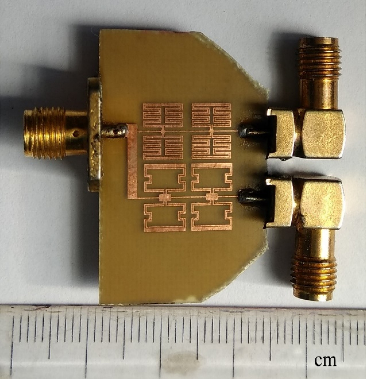
Fig. 11. Photograph of the experimental diplexer prototype.
The comparative simulated and measured S-parameter versus frequency graph for the proposed diplexer is presented in Fig. 12.

Fig. 12. The comparative simulated and measured S-parameter versus frequency graph for the proposed diplexer.
The measured passband center frequencies are 3.5 and 5.6 GHz with −3 dB FBW of 21.21 and 13.29%, respectively. The measured insertion loss |S 21| at f 1 and f 2 are −0.87 and −1.25 dB, respectively. Return loss |S 11| > 16 dB at f 1 and >15.1 dB at f 2.
The measured results are in compliance with the simulated results, which shows that the proposed diplexer is viable for practical use. The isolation parameter |S 23| versus frequency plot for the proposed diplexer is shown in Fig. 13. It can be seen from the graph that for the whole concerned frequency range from 2.5 to 8 GHz, measured isolation between both the channels is >32.5 dB. The proposed diplexer's physical parameters, structure fabrication complexities and execution are compared with other previously reported diplexers in Table 4.

Fig. 13. Comparative simulated, equivalent circuit model and measured isolation coefficient of port2 and port3 for the proposed diplexer.
Table 4. Comparison between the proposed diplexer and reported diplexers.

From comparison table it can be seen that the proposed diplexer has the merit of compactness, wider passbands, low insertion loss at the passbands, and high isolation.
Conclusion
This paper presents the design of a compact planar via-free CRLH TL diplexer which covers measured frequency band of 3.15–3.93 GHz (−3 dB bandwidth) and 5.19–5.97 GHz (−3 dB bandwidth). The proposed diplexer hence covers the standard bandwidth requirement of WiMAX and WLAN IEEE standard. In addition, the size of the diplexer including 50 Ω feed line is 18 × 15 mm2. The diplexer has a −28 dB upper stopband rejection level from 6.7 to 8.0 GHz. Because of the compactness, low-cost design fabrication and good in performance, the proposed diplexer prototype may find suitability in many modern small-sized wireless communication systems.
Author ORCIDs
Abhishek Kumar 0000-0001-8471-7006.
 Abhishek Kumar is currently pursuing his Ph.D. as an Institute Research Fellow in the Department of Electronics and Communication Engineering from the Birla Institute of Technology, Mesra, Ranchi, India. He received his graduate degree (B.Tech.) in Electronics and Communication Engineering from Biju Patnaik University Technology (BPUT) Odisha, India, in 2011. He completed his postgraduate (M.E.) degree in Wireless Communication from the Department of Electronics and Communication Engineering, Birla Institute of Technology, Mesra, Ranchi, in 2015. His research interests include design and development of microwave circuits using left-handed metamaterials for wireless communication systems.
 Dileep Kumar Upadhyay is currently working as an Assistant Professor in the Department of ECE, Birla Institute of Technology, Mesra, Ranchi since August 2007. He has received his graduate degree (B.Tech.) in Electronics and Communication Engineering in 2005 from Uttar Pradesh Technical University (UPTU), Lucknow and completed his postgraduate (M.E.) degree in Wireless Communication from the Department of Electronics and Communication Engineering, Birla Institute of Technology, Mesra, Ranchi, in 2007. He has received his Ph.D. (Engg.) degree in March, 2014 on the topic “Characterization and experimental verification of new microwave circuits, using metamaterials in wireless communications”, from the Department of Electronics and Communication Engineering, Birla Institute of Technology, Mesra, Ranchi. His current research interests include RF circuit design, design and development of metamaterial-based microwave circuits, defected ground plane and fractal geometry based microwave circuits for the applications in wireless communication systems.


