I. INTRODUCTION
The current upsurge in wireless communication systems has forced antenna engineering to face new challenges, which include the need for wide bandwidth, small-size, high-performance, robustness, ease of mounting on host surface, and low-cost antennas. To have compatible uses for wide range of applications by fulfilling mobility requirement and holding up the performance as well as the capability of obtaining dual and triple frequency operations are challenges [Reference Volakis, Chih and Fujimoto1]. Printed-IFA antennas offer an attractive solution to compact and ease-low-cost design of modern wireless communication systems due to the above advantages. Printed inverted-F antenna (IFA) is a simple and compact radiator, however; it cannot radiate efficiently near a perfect electric conductor (PEC) ground plane due to reverse image currents. Also, printed-IFA antennas suffer from a number of disadvantages as compared to conventional non-printed antennas. Some of their major drawbacks are narrow bandwidth, λ/4 length, low gain, and surface wave excitation that reduce radiation efficiency. To solve the problem of their narrow bandwidth, several techniques can be used [Reference Anguera, Sanz, Mumbrú and Puente2–Reference Bhatti, Im and Park4]. A thicker substrate with a low dielectric constant or a ferrite composition provides a wider bandwidth but this approach leads to no low-profile designs and an increase in size. Non-contacting feeding methods such as proximity/aperture coupled can be used to improve the impedance bandwidth, but this is difficult to fabricate. Another possibility is multi-resonator stack configuration with the inconvenience of resulting large thickness prototype [Reference Chaimool, Chung and Akkaraekthalin5].
To overcome the problem of large size, basic antenna miniaturization techniques can be classified into lumped-element loading, the use of the antenna geometry, which can be also used in order to make antennas smaller [Reference Anguera, Puente, Martínez and Rozan6–Reference Anguera, Boada, Puente, Borja and Soler9], material loading, the use of ground planes, short circuits, the antenna environment, as applied antenna on electromagnetic band-gap structures (EBGs). Based on this, many attempts to design compact antennas have been made in the past [Reference Wong and Chang10]. Among various EBG structures, uniplanar EBG designs such as mushroom-like structure [Reference Yang and Rahmat-Samii11] received great potential for wireless communication systems because of their low-profile configurations. One important application of EBG structures is to serve as the ground plane for low-profile antennas [Reference Yang and Rahmat-Samii12–Reference Yang and Rahmat-Samii16]. The EBG structures are usually periodic arrangements of metallic or dielectric elements that exhibit band-gap characteristics which are sensitive to the permittivity, thickness of the substrate, and most importantly to EBG geometry. The important properties of EBG are the ability to guide and control the propagation of electromagnetic waves, suppression of surface waves within the band-gap range and hence improvement of antenna performance by reducing cross polarization, back radiation and mutual coupling [Reference Assimonis, Yioultsis and Antonopoulos17–Reference Abedin, Azad and Ali19]. Most of the researches were focused on three-dimensional EBG structures, which are complicated, heavy, and difficult to integrate with microwave circuits. To avoid complexity, planar 2D EBG-like mushroom shape, split ring resonator (SRR)-like shape, spiral shape, etc. were suggested [Reference Yamamoto and Nojima20–Reference Duan, Qu and Hou23].
In this paper, the performance of L-loaded printed-IFA antenna with meandering shape at the open end near the edge of a PEC ground plane is first investigated. Then different shapes of mushroom-like high-impedance surface (HIS) as EBG structures are used to improve the antenna parameters such as broaden bandwidth, efficiency, and reduce electrical size. Satisfactory results are obtained. All simulations are carried out using the EM commercial simulator, HFSS ver. 13.0.
II. DESIGN OF PRINTED-IFA ANTENNA
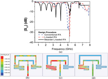
This section gives the details of the design procedure of the proposed multiband printed IFA antenna. It starts with the design of a conventional printed-IFA that operates at 5.2 GHz, over a conventional ground plane as shown in Fig. 1(a). The printed IFA dimensions are length L 1 = 21.75 mm with shorting wall size W 1 = 7.4 mm and ground plane size L sub × W sub = 35 × 45 mm2. The distance between the feed and the short end L op = 16.5 mm with L sep and W sep are 6.5 × 4.5 mm2 and all transmission line widths are 2 mm. Then, two different approaches were investigated to introduce more bands to the printed-IFA. The first approach is using an L-loaded printed-IFA as shown in Fig. 1(b) with length and width L 2 × W 2 = 30 × 12 mm2, this element acts as a parasitic element, which helps to enhance the bandwidth. The antenna resonates at dual resonant frequencies 3.1 and 5.2 GHz. It may be noted that the dual resonance frequencies are independent. Finally, to reduce the electrical size of L-loaded IFA antenna, additional inductors are added. Two meandering shapes with two unit cells at both open ends of the L-loaded IFA as shown in Fig. 1(c) are added. Multiband with reduction in electrical antenna size is created with approximately same antenna parameters. Three antenna design steps are shown in Fig. 2. Figure 2 shows that the conventional IFA resonates at 5.2 GHz, while additional resonant frequency is added by loading L-shaped at 3 GHz and keeping the first resonant slightly unchanged. The antenna is resonant at multiband by adding a meander line at the open ends of L-loaded IFA at 1.4, 2, 2.8, 3.2, 4, and 5.2 GHz with poor antenna matching. The current distribution for selected resonant frequencies at 1.4, 2, and 5.2 GHz is shown in Fig. 2.

Fig. 1. Configuration of (a) conventional IFA, (b) L-loaded IFA, and (c) meandered L-loaded IFA.

Fig. 2. Simulated |S11| of the design antenna procedures with conventional ground.
III. DESIGN OF DIFFERENT SHAPES OF EBG
The design of a uniplanar structure of an HIS with compactness is a challenge nowadays. The absence of ground connecting vias, makes the challenge significant, but not impenetrable. Owing to the frequency sensitiveness of surface impedance of periodic structures such as EBG, the configuration must be designed carefully.
Miniaturization and good performance are difficult to achieve simultaneously, particularly at lower frequencies. Some studies have been reported, which improve the performance of patch antennas using periodic structures [Reference Shafai8, Reference Wong and Chang10]. In fact, it is well known that a patch antenna on a high dielectric constant substrate is a highly inefficient radiator due to surface wave losses and has a very narrow bandwidth. However, significant effort has been recently made to realize high performance antennas employing electromagnetic EBG structures printed on high permittivity substrates. High-impedance electromagnetic surfaces have been studied by Sievenpiper [Reference Sievenpiper, Zhang, Jimenez Broas, Alexopolous and Yablonivitch7]. In his approach, HISs (in general) consist of a lattice of metal plates, connected to a solid metal sheet.
 $$2W=\lambda _{guid}\comma \;$$
 $$W/p=0.8-0.9\comma \;$$
where W, P, and λguid are side length, periodicity, and guided wavelength, respectively [Reference Sievenpiper, Zhang, Jimenez Broas, Alexopolous and Yablonivitch7–Reference Yang and Rahmat-Samii12].
In this paper, different shapes of HIS structures were introduced as mushroom, ring, SRR, and spiral shape cells, respectively, as shown in Fig. 3 to produce wide or dual band gaps and as a means to suppress surface waves effectively [Reference Fan, Feng, Hu, Zhang and Hao18–Reference Yamamoto and Nojima20]. The configurations of transmission lines over the 7 × 5 cell arrangement used to test the proposed EBG structures are shown in Fig. 4. The design consists of a one layer substrate; printed on an FR4 board of thickness 1.6 mm. This figure represents the metallic periodic structure, which is etched on the dielectric substrate. The main element of this EBG square lattice has side length W = 7.5 mm and periodicity P = 8 mm. The SRR is etched with a gap width and length g = 1 mm. Then, a ring shape is etched with strip width equal to separation air gap g = 1 mm. Finally, one arm spiral is created to introduce the second band gap. The bandwidth of the band-gap depends on the width of the arm, dielectric constant, and height of the substrate when using 50 Ω broadband transmission lines. The transmission responses of these configurations are shown in Fig. 5. This figure shows that the square shape has one band gap starting from 4.5 up to 8 GHz, while, SRR creates two band-gaps at 4.5–5.5 GHz and from 7.5 to 8 GHz, the two split ring EBG shape has a dual band gap starting, respectively, from 2.5 to 4 GHz and from 6.5 to 8 GHz. Finally, spiral EBG shapes create a multiband gap, one at lower frequency from 1.7 to 2.3 GHz and the other starting, respectively, from 4 to 8 GHz.

Fig. 3. Different unit cell shapes of EBG ground plane mushroom, SRR, ring, and spiral.

Fig. 4. Different shapes of EBG structures (a) mushroom, (b) SRR (c) ring, and (d) spiral.

Fig. 5. The transmission response for EBG ground, mushroom, SRR, ring, and spiral.
IV. PRINTED-IFA WITH EBG GROUND PLANE
The last step in the proposed antenna design is replacing the conventional antenna ground by 5 × 7 patch arrays of HIS EBG structure to suppress the surface waves and to increase the number of resonant frequencies by means of coupled resonators effect. The EBG lattice is arranged under the radiator, Fig. 6. Inductive and capacitive values are added to reduce antenna size and create multiband. Different shapes of uniplanar EBG ground plane, SRR shape, ring shape, spiral shape, and mushroom shape are applied as a ground plane; all cells have same dimensions and periodicity. The design started by applying these shapes of EBG ground plane on single printed IFA is shown in Fig. 1(a). The simulated reflection coefficient is shown in Fig. 7. Multi-bands are generated at low frequency especially <3 GHz by using spiral EBG, while at high frequency the spiral and ring shape give good performance. Then, the L-loaded IFA is applied on different EBG shapes ground plane shown in Fig. 1(b). Simulated S11 is shown in Fig. 8, the number of antenna resonances is increased especially by using spiral and ring shapes, which gives good performance.

Fig. 6. Printed meander L-loaded IFA with different EBG configurations (a) SRR, (b) ring, and (c) spiral.

Fig. 7. |S11 | of the printed IFA antenna on different uniplanar EBG ground plane shapes.

Fig. 8. |S11 | of the printed L-loaded IFA antenna on different uniplanar EBG ground plane shapes.
By loading meander shapes at the open end of L-loaded IFA antenna the number of resonances is increased and antenna matching is improved as shown in Fig. 9. Spiral, ring, and SRR give good performance, respectively, with good antenna matching. These results could be explained as a spiral shape creating band-gap at lower frequency from 1.5 to 2.5 GHz and band-gap opened from 4 to 8 GHz, while ring EBG shape ground plane creates a broad band-gap from 2.5 to 4 GHz and another band-gap opened from 6 GHz. Hence, the number of resonant frequencies is increased in this region and by adding inductance and capacitance under the radiator the antenna size is reduced and antenna matching is improved.

Fig. 9. Comparison of| S11 | of the printed meandered L-loaded IFA antenna on different uniplanar EBG ground plane shapes.
V. SIMULATION AND MEASUREMENT RESULTS
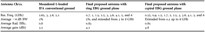
The optimized multiband proposed antennas, presented in the previous section, were fabricated on an FR4 substrate (ɛr = 4.4, h = 1.6 mm, and tan δ = 0.02). From the above results, ring and spiral shape ground plane were selected due to their good performance to be fabricated for both configurations, L-loaded IFA with and without meander shape. The fabricated antenna structures for both upper and lower layers are shown in Fig. 6. The comparison between simulated and measured reflection coefficient is shown in Fig. 10. The measurements agree well with EM simulations, and show that the operating bands have return loss better than −6 dB. When these EBG structures were applied as printed IFA ground planes the antenna resonant frequencies were reduced due to the capacitive effects that were generated between the two combined structures (Fig. 11). Multi resonant frequencies are achieved at 1.1, 1.58, and 2.49 GHz and the bandwidth extended from 3.5 to 5.5 GHz because of the number of band-gap stops shown in Fig. 5 for both L-loaded PIFA and meandered L loaded IFA, respectively. The simulated antenna gain with and without EBG ground plane is shown in Fig. 12. Figure 12 shows that the antenna with spiral EBG ground plane has average gain greater than the other two shapes. However, the antenna with ring EBG ground plane has gain higher at frequency band from 3 to 4 GHz. The fabricated antenna is shown in Fig. 13. The simulated antenna parameters, meandered L-loaded IFA with conventional ground, ring EBG, and spiral ground are shown in Table 1.

Fig. 10. Comparison between measured and simulated |S11| of L-loaded IFA antenna with and without meandered shape on ring EBG ground plane.

Fig. 11. Comparison between measured and simulated |S11| of meandered L-loaded IFA antenna with and without meandered shape on spiral EBG ground plane.

Fig. 12. Simulated antenna gain for the meandered L-loaded printed IFA with and without EBG ground plane.

Fig. 13. Fabricated antennas, top layer: (a) L-printed-IFA, (b) meander loaded printed IFA, bottom layers: (c) ring-EBG ground plane, and (d) spiral-EBG ground plane.
Table 1. Simulated antenna parameters.
Finally, simulated radiation patterns for three antenna planes (ZX, ZY, and XY) are also studied. Comparison of radiation pattern between the proposed antenna with and without EBG ground plane at four different resonant frequencies 1.8, 2.4, 3.5, and 5.2 GHz are presented in Table 2.
Table 2. Simulated radiation patterns, antenna with conventional ground ![]() , antenna with ring EBG ground
, antenna with ring EBG ground ![]() , and Spiral EBG ground
, and Spiral EBG ground ![]() . Axes are shown in Fig. 1.
. Axes are shown in Fig. 1.

VI. CONCLUSION
Multiband compact printed-IFAs for internal mobile phone antenna and wireless applications have been proposed and studied. Three different shapes of EBG rather than mushroom were studied as printed antenna ground plane. It can be concluded that spiral and ring EBG structures prototype improved antenna matching, reduced the antenna size, and generated extra number of resonant frequencies. The operating frequencies are 0.9, 1.57, and 2.48 GHz, resonant frequencies extended from 3.5 up to 8 GHz for L-loaded printed-IFA spiral EBG ground plane, while lower frequency improved and higher frequency was slightly unchanged by using meandered L-loaded IFA. EBG-printed IFA provides around 80% size reduction, while the antenna characteristics remain almost unchanged. The proposed technique in this paper can be extended to create more operating bands.
ACKNOWLEDGEMENT
This research was funded by the National Telecommunications Regulatory Authority, (NTRA), Ministry of Communication and Information Technology, Egypt.
 Dalia M. Elsheakh received the B.S., M.S., and Ph.D. degrees in Electrical and Communication Engineering from Ain Shams University, Cairo, Egypt, in May 1998, September 2004, and October 2010, respectively. Her master's thesis was about the design of microstrip PIFA antennas for mobile handsets. Her Ph.D. dissertation was entitled, ‘Electromagnetic Band-Gap (EBG) Structure for Microstrip Antenna Systems (Analysis and Design).’ From 2008 to 2009, she was an Assistant Researcher in the Hawaii Center for Advanced Communications (HCAC), College of Engineering, the University of Hawaii at Manoa, Honolulu. She holds one patent, has published 21 papers in peer-refereed journals and 22 papers in international conferences in the area of microstrip antenna design. Her current research interests are in microstrip antennas theory and metamaterials design and electromagnetic wave propagation. She participates in many research projects at the national and international levels as Egypt-NSF-USA joint funds program and the European Committee Programs FP7 program, STDF and ITIDA-ITAC.
 Esmat A. Abdallah graduated from the Faculty of Engineering and received the M.Sc. and Ph.D. degrees from Cairo University, Giza, Egypt, in 1968, 1972, and 1975, respectively. She was nominated as Assistant Professor, Associate Professor and Professor in 1975, 1980, and 1985, respectively. She has focused her research on microwave circuit designs, planar antenna systems, and non-reciprocal ferrite devices, and recently on EBG structures, UWB components and antenna and RFID systems. She acts as a single author and as a coauthor on more than 127 research papers in highly cited international journals and in proceedings of international conferences in her field, such as IEEE Trans., Antenna Propagat. and Microwave Theory Tech., Microwave and Optical Technology Letters, etc. She participates in many research projects at the national and international levels such as Egypt-NSF-USA joint funds program and the European Committee Programs FP7 program, etc. She is also a reviewer for many international societies.