


Introduction
Past few decades, a number of slot antennas and annular ring patch antennas are reported to get better performances, mostly for wideband and circular polarization applications. Slot antennas have miniaturization potential and reasonably wide bandwidth characteristics. However, the annular ring patch antenna has small dimensions as compared with other patch shapes antenna resonating at the same frequency. An annular ring patch antenna with and without slots becomes the subject of great interest for the engineering researchers due to their various properties which are reported in [Reference Kanaujia and Vishvakarma1–Reference Singh, Gangwar and Kanaujia9]. Paper [Reference Zhao, Gai, Liu, Xiong, Chen and Jiao10] presents, a reconfigurable annular ring slot antenna with a switchable polarization which is achieved by turning the pin diodes on or off and circularly polarized (CP) radiation is obtained by introducing protruded slots and strips in the annular ring slot structure. In [Reference Row11], a CP square-ring slot antenna is proposed which is fed by a series microstrip-line coupled to the two orthogonal sides of the square ring slot to achieve circular polarization characteristics. An annular slot antenna with a cross-shaped feed line has been reported in [Reference Jang12]. A new design for a dual-frequency dual CP is achieved in [Reference Bao and Ammann13] by using a single-layer microstrip-fed configuration coupled to a modified annular slot antenna. To achieve a compact size and circular polarization, a number of slot combinations are reported in [Reference Wong, Huang and Chen14–Reference Kumar, Kanaujia, Sharma, Khandelwal and Gautam22]. A novel symmetric-aperture antenna is proposed in [Reference Nasimuddin, Chen and Qing23] for broadband CP radiation. In [Reference Chen and Yung24], a dual band and the dually polarized antenna are achieved by two loaded spiral slots in the ground plane. The dual-sense polarization operation is also achieved by using a circular patch with eight curved slots and a disk-loaded coaxial probe in [Reference Yu, Gong, Wan and Chen25]. A bent feeding configuration and three slots, together with a T-shaped and two inverted L-shaped slots in the ground plane are proposed in [Reference Wang, Shih and Chen26] for dual-sense polarization operation. A dual band CP spiral slot loaded antenna is proposed in [Reference Bao and Ammann27].
Recently, there was a developing research activity on many microstrip line fed printed wide-slot antennas because of their good impedance characteristics. In order to generate CP wave through a single feed slot antenna which can radiate linearly polarized wave, two orthogonal modes of equal amplitude and 90° phase difference are required to be introduced. This can be achieved by one of the methods of etching the ground plane unevenly with respect to the feed position. Structurally small, dual wide frequency band, and dually polarized microstrip antennas are widely utilized in handheld portable devices and in compact mobile communication systems. A number of applications is needed, in addition, to small size CP microstrip antennas where the antenna size could be the main consideration, such as for satellite, radar, mobile communication and portable wireless devices.
In this paper, a new compact design of microstrip line fed printed antenna using FR-4 substrate with a modified square ring slot on the ground plane is proposed and investigated. The modified square ring slot consists of four unequal linear slots; designed for dual wide-band operation with CP radiations. The impedance bandwidths for dual frequency bands are 3000 and 3830 MHz with 3 dB ARBWs of 1700 and 400 MHz, respectively. The proposed antenna is mostly useful in C band and Ku band applications. A number of satellite communications transmissions, several Wi-Fi devices, IEEE 802.11a, various cordless telephones, and a few weather radar systems come under the C band applications. However, Ku band is mainly used for satellite communications, mostly for the downlink utilized by direct broadcast satellites to broadcast televisions, and for specific applications like NASA's Tracking Data Relay Satellite used for both space shuttle and International Space Station Communications.
Antenna structure and design
The proposed antenna has main advantages of its compact size with an overall area of 18 mm × 18 mm. It uses easily available dielectric material FR-4 (ε r = 4.4) of 1.6 mm thickness (h) for fabrication. The geometry of the proposed antenna with top and side view is represented in Figs 1(a) and 1(b), respectively. The antenna structure contains a modified square ring slot on the ground plane with a 50 Ω microstrip feed line on opposite side. The microstrip line feed of width W f with an optimized value of length L f is placed at the center of antenna side.

Fig. 1. Geometry of the proposed antenna; (a) top view, and (b) side view.
The modified square ring slot is made up of four unequal linear slots which are combined with opposite sides of a square ring of inner sides W in × L in. All four linear slot have width of W 1, W 2, W 3, and W 4 with length L 1, L 2, L 3, and L 4, respectively. This slot structure is mainly designed for obtaining dual wide-band and CP antenna. The unequal linear slots, those are united with square ring slot are the main cause of generating CP waves. Detailed dimensions of the proposed antenna are listed in Table 1.
Table 1. Dimensions of the proposed antenna

The fabricated image of the top and bottom view of the proposed antenna is represented in Figs 2(a) and 2(b), respectively. The optimized results for the proposed modified square ring slot antenna are investigated by the different mean slot circumferences. That shows the input impedance is a pure resistance when the mean circumference of the square ring slot is about 0.7 times of the operating free-space wavelength [Reference Row11]. This factor could be distinct due to the different feeding methods for the slot antennas. By the given design frequency, the outer and inner side lengths of the square ring slot can be decided by the expressions [Reference Row11].
 $$W_{{\rm out}},L_{{\rm out}}\; \sim \displaystyle{{\; 0.7\; \lambda _o} \over 4} + d,$$
 $$W_{{\rm in}},\; L_{{\rm in\;}} \sim \displaystyle{{0.7\; \lambda _o} \over 4}-d,$$
where d is the width of the conventional square ring slot.

Fig. 2. Fabricated image of proposed antenna; (a) top view, and (b) bottom View.
From several simulation results for the substrate material with a fixed thickness of 1.6 mm and different permittivity ranged from 1.0 to 10, the required design frequency can be approximately expressed as [Reference Bao and Ammann13]
 $$\displaystyle{{\,f_o \sim \; c_o} \over {2.\pi. K.\sqrt {\varepsilon _e}}}, $$
where K is the mean circumference of the square-ring slot and εe is the substrate effective dielectric constant. In case when the substrate thickness is much higher or lower than 1.6 mm, equation (3) is not appropriate.
The suitable impedance matching condition caused by the addition of four unequal linear slots with the square ring slot in the ground plane is also studied and examined as shown in Fig. 3. The curve for design (a) represents the simulated result for return loss of the antenna with a simple microstrip line fed in the opposite side of the ground plane. It is observed that without a ring slot, resonance is obtained around 22 GHz with low bandwidth. Furthermore, design (b) illustrate the square ring slot is inserted in the same ground plane, keeping other parameters are the same. Insertion of the square ring slot results in a sudden shift of the resonance frequency toward the lower frequency range of 12.5 GHz, and it also slightly increases the bandwidth with a large return loss value as depicted in the curve for design (b). Finally, the inclusion of the unequal linear slots to the opposite sides of the square ring slot in the design (c), also increases the area of the slot. It significantly generates two resonance frequencies with wide impedance bandwidths. Furthermore, the curve for proposed design illustrates desirable resonant bands at 5.9 GHz 12.8 GHz. This will show a good miniaturization of a slot antenna.

Fig. 3. Simulated return loss against frequency for the same ground plane; (a) without a ring slot, (b) with square ring slot, and (c) with a modified ring slot.
Parametric study
The proposed antenna is fabricated with optimized parameters and measurement has been performed with the help of a vector network analyzer. A parametric study of the proposed antenna was conducted by varying only one parameter at a time, while other parameters value was kept unvarying. To achieve desired operating bands with circular polarization, each antenna parameters are optimized. The effects of varying some antenna parameters for dual wide-band CP operation of the proposed antenna are given in this section. To analyze optimized value for given parameters, all simulated results are shown by various plots.
Effects by varying slot widths, W 1, W 3
The simulated results of the antenna return loss and the axial ratio with the variation of the modified square ring slot widths, W 1 and W 3 are plotted in Figs 4(a) and 4(b), respectively. The values of W 1 and W 3 were varied from 1 to 3 mm. By increasing values of slot widths, impedance bandwidths appreciably vary, while the results of the axial ratio are not significant. At W 1 = W 3 = 2 mm, the antenna had considerable CP radiation over the required bands.

Fig. 4. Effect of varying slot widths, W 1, W 3; (a) return loss, and (b) axial ratio.
Effects by varying slot lengths, L 2, L 4
The values of modified square ring slot lengths, L 2 and L 4 also affect the antenna's performance. The variation of the return loss and the axial ratio with varying slot lengths, L 2 and L 4 of the antenna are plotted in Figs 5(a) and 5(b), respectively. The values of L 2 and L 4 were varied from 3.5 to 4.5 mm together with fixed values of their width. At slot lengths of 3.5 mm, both the bands are shifted upper side of the frequency with linear polarization. After increasing the value to 4 mm two resonant frequencies create dual wide-band with CP radiation of the antenna. The performance of the antenna at 4.5 mm of the slot lengths is not up to the level for desired bands with the required axial ratio.

Fig. 5. Effect of varying slot lengths, L 2, L 4; (a) return loss, and (b) axial ratio.
Effects by varying inner slot dimensions, W in, L in
Different values of the inner sides W in × L in of the modified square ring slot affects the antenna's performance. The inner width W in and inner length L in are varied to improve the axial ratio characteristic. The return loss characteristics and ARBW for different values of W in and L in are shown in Figs 6(a) and 6(b). It is observed that the desired dual wide-band with good ARBWs achieve at the value of W in = L in = 4 mm.

Fig. 6. Effect of varying inner ring slot sides, W in, L in; (a) return loss, and (b) axial ratio.
Effects by varying feed length, L f
The microstrip line feed length of L f varied from 9 to 10 mm. By increasing the value of feed length, impedance bandwidths decrease with insignificant ARBWs. For feed length of 9.5 mm, the antenna had good impedance bandwidths for both band and good ARBWs, as shown in Figs 7(a) and 7(b), respectively.

Fig. 7. Effect of varying feed length, L f ; (a) return loss, and (b) axial ratio.
It is clearly analyzed from a parametric operation that the center frequencies of desired impedance bandwidths are tuned independently within the first operating range from 4.38 to 7.38 GHz and second operating range from 11.78 to 15.61 GHz. By varying linear slot widths W 1 and W 3, inner slot dimensions, W in, L in, higher center frequency will be tuned. To improve ARBW of the second band, dimensions of the square slot should be minimized. Consequently, first ARBW must be degraded from the desired range.
Results and discussion
The results of the proposed antenna are discussed in this section. Simulation of the impedance characteristic and radiation characteristic for the proposed antenna is carried out by using HFSS software and measurement with Agilent vector network analyzer of PNA-L series no. N5230A. Figure 8 illustrates the results of return loss with frequency. Two wide-bands appeared in the result of return loss, due to different modes (TM11 and TM21) are excited as the proposed antenna has been simulated. The result shows an impedance bandwidth (return loss >10 dB) of 50.88% (from 4.38 to 7.38 GHz) at 5.9 GHz of center frequency and 29.92% (from 11.78 to 15.61 GHz) at 12.8 GHz of center frequency for lower and upper bands, respectively. Simulated data for return loss show good agreement with measured results.

Fig. 8. Variation of return loss with frequency.
The measured and simulated axial ratios curves of the proposed antenna are shown in Fig. 9. By adjusting the dimensions of various slots properly, different CP waves are obtained at the TM11 and TM21 modes, respectively. It is observed that the antenna shows dual wide-band of CP as RHCP wave in the lower and upper bands of the impedance bandwidth. The values for ARBW (axial ratio <3 dB) are about 26.4% (from 5.6 to 7.3 GHz) for the lower band and 3.0% (from 13.2 to 13.6 GHz) for the upper band with the center frequency at 6.5 and 13.4 GHz, respectively. It is also found that minimum axial ratio values are 0.9 and 0.4 dB for the lower and upper bands, respectively.

Fig. 9. Variation of axial ratio with frequency.
The proposed antenna consists of single feed and asymmetric structure around ring slot on the ground plane, which will generate two orthogonal field distributions of the same magnitude with 90° phase difference for CP radiation as shown in Fig. 1. From Fig. 10(a), it is found that the strong surface current is distributed over the modified square ring and feed line at 6.5 GHz which generates TM11 mode. It indicates the direction of surface current vectors at time phase ωt = 0° in −x direction and at time phase ωt = 90° in −y direction, which are equal in magnitude and opposite in time phase to 180° and 270°, respectively. Figure 10(b) reveals the surface current at 13.4 GHz which generates TM21 mode and mainly distributed on the modified square ring slot on the ground plane. It shows the direction of the surface current vector at time phase ωt = 0° in +y direction and at time phase ωt = 90° in −x direction, which is equal in magnitude and opposite in time phase to 180° and 270°, respectively. This suggests that the designed antenna have right hand CP (RHCP) for boresight (+z) and left hand CP (LHCP) for backside (−z) direction for both wide-bands. The surface currents at TM11 mode varies one-half wavelengths along slot length and width and at TM21 mode, they vary along slot width and show two half wavelengths variations.

Fig. 10. Simulated surface current density at; (a) 6.5 GHz, and (b) 13.4 GHz.
Variation of gain with the frequency of the proposed antenna is shown in Fig. 11. It is observed that the antenna gives a measured peak gain of 3.2 dBic for lower and 3.4 dBic for upper operating bands. The radiation pattern of the proposed antenna in xz-plane and yz-plane at 6.5 GHz are shown in Figs 12(a) and 12(b), respectively, and Figs 12(c) and 12(d) show the radiation pattern in xz-plane and yz-plane at 13.4 GHz, respectively. From the close observation of radiation pattern in lower and upper bands, RHCP wave is generated in both planes. The proposed antenna has bidirectional radiations. For +z direction, the antenna is RHCP radiation and for −z direction, the antenna is LHCP radiation. Both xz and yz-planes are in good agreement at the boresight (+z) and backside (−z) direction. However, cross-polarization level is sufficiently low in roadside radiation.
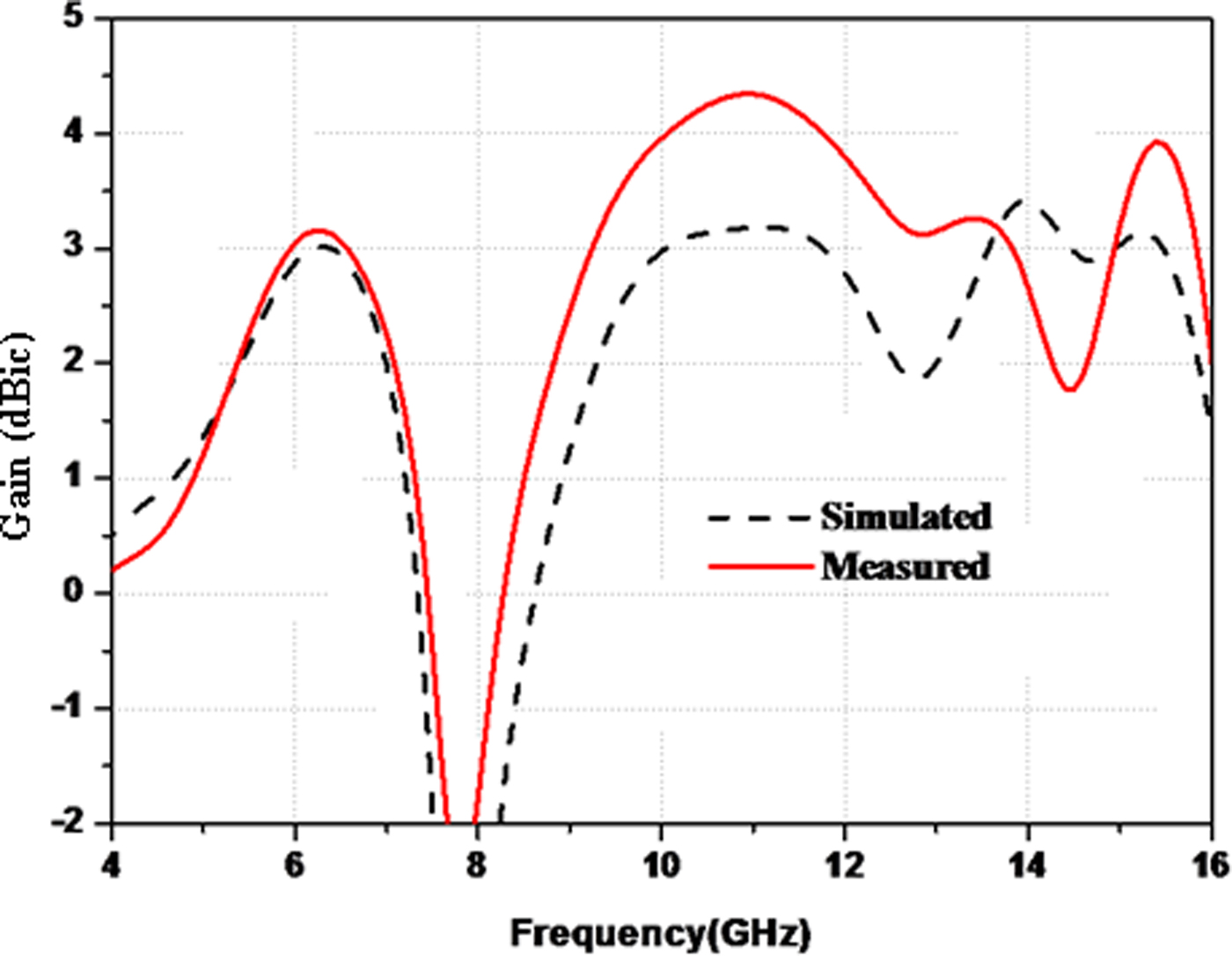
Fig. 11. Variation of gain with frequency.

Fig. 12. Radiation pattern at 6.5 GHz in; (a) xz-plane, and (b) yz-plane, and at 13.4 GHz in; (c) xz-plane, and (d) yz-plane.
Table 2 illustrates the comparison of the proposed dual wide-band CP antenna and the previous CP antennas. It shows that this antenna has a compact size and good impedance bandwidths with suitable ARBWs. The measured peak gain of the proposed antenna is also appropriate as compared with listed antennas.
Table 2. Comparison between various parameters of different CP slot antennas

Conclusion
A compact, dual wide-band CP microstrip antenna, printed on the less expensive FR-4 substrate is presented in this paper. Dual wide impedance bandwidth and ARBW is obtained by using a single-layer microstrip line fed configuration coupled to a modified square ring slot antenna. The RHCP radiation for both bands is obtained by using four unequal linear slots which augment the square ring slot. The proposed antenna has wide upper and lower frequency bands of 3000 and 3830 MHz at 5.9 and 12.8 GHz of center frequencies, respectively. The 3 dB ARBWs of 26.4 and 3% are obtained for lower and upper bands, respectively. The measured axial ratio values are obtained at 0.9 and 0.4 dB at TM11 and TM21 modes, respectively. The results obtained by simulation are acceptable and are in close agreement with the measured results. Differences shown in the measured and simulated results are due to the fabrication imperfections and measurement errors. The proposed antenna has potential applications in C and Ku bands communications which mostly include satellite communication, radar systems, Wi-Fi, and broadcast services.
Acknowledgements
Dr. Binod K. Kanaujia thankfully acknowledges DBT & COE project funds for providing infrastructure support and DST-PURSE, Govt. of India & UPE II ID: 340, JNU for providing support throughout this work.
 Shilpee Patil received her B.Tech. degree in Electronics & Communication Engineering from AKTU (formerly UPTU), Lucknow, India, the M.Tech. degree in Digital Communication from GGSIP University, Delhi, India, in 2009. She is currently pursuing her Ph.D. degree in Electronics Engineering from AKTU, Lucknow, India. Her research interests are microstrip antennas, slot antennas, and circularly polarized microstrip antenna for wireless communications.
 Anil Kumar Singh was born in Jamalpur, Mirzapur (UP), India in 1976. He has completed M. Tech. Degree in Instrumentation and Control Engineering from NITTTR Chandigarh, India and Ph.D. degree on Some Study on Annular Ring Microstrip Antenna from Electronics Engineering Department, Indian School of Mines (ISM), Dhanbad, (India). He joined the Department of Electronics and Instrumentation Engineering, Institute of Engineering and Technology, M. J. P. Rohilkhand University, Bareilly as a lecturer in 2002. He has published more than 20 papers in national and international journals and conferences. His current research interest includes design and analysis of microstrip antennas.
 Binod Kumar Kanaujia is working as Professor in the school of computational and integrative sciences, Jawaharlal Nehru University, New Delhi since August 2016. Dr. Kanaujia completed his B.Tech. in Electronics Engineering from KNIT, Sultanpur, India in 1994. He did his M.Tech. and Ph.D in 1998 and 2004, respectively, from the Department of Electronics Engineering, I.I.T. B.H.U., Varanasi, India. He has a keen research interest in design and modeling of reconfigurable and circular polarized microstrip antenna. He has been credited to publish more than 150 research papers with more than 430 citations with h-index of 12 in peer-reviewed journals and conferences. He successfully executed 04 research projects sponsored by several agencies of Government of India i.e. DRDO, DST, AICTE, and ISRO. He is a member of several academic and professional bodies i.e. IEEE, Institution of Engineers (India), Indian Society for Technical Education and Institute of Electronics and Telecommunication Engineers of India.
 R.L. Yadava is working as Professor in the Department of Electronics and Communication Engineering, Galgotias College of Engineering and Technology, Greater Noida, Uttar Pradesh. He received his Ph.D. degree in Electronics Engineering from I.I.T. B.H.U., Varanasi, India. He joined Vellore Institute of Technology (VIT) University, Vellore, in 2001 and served as Head of the Microwave Division, Coordinator (R&D) and Coordinator (UG) of Electrical Sciences. He has organized several guest lectures, short-term training programmes, and conferences in the field of microwave and antennas. His research areas include waveguides, microwaves, and microstrip antennas. Presently, he is working on fractal antennas, superstrate loaded and AFFS antennas, and RECTENNAS in collaborations with ISM Dhanbad and other reputed Universities. He has 65 publications to his credit in International/National journals, conferences, and symposiums. He is associate editor of Journal of Information, Intelligence and Knowledge, USA and also a member of ISTE, STE, SEMCE(I), and IEEE.


