


I. INTRODUCTION
Radiofrequency (RF) power amplifiers find many applications in modern electronics typically in broadcast systems, communication systems, satellite communication, and radar systems [Reference Raab1, Reference Florian, Ciganani, Santarelli and Filicori2]. Typically high-power RF amplifiers are designed in such a way that the output power is combined from many identical transistor stages, each delivering the fraction of the output power, due to the limited power available from a single transistor [Reference Epp, Hoppe, Khan and Stride3–Reference Johansson and Fritzin5]. Therefore, the critical aspect in the design of RF power amplifiers is the correct dimensioning of the power dividers/combiners that must operate in sufficient bandwidth and are able to handle rated output power. Also an adequate impedance match to the impedance of applied semiconductors is required.
In a classic approach to the design of multistage high-power amplifiers the dividing/combining feeding networks are designed with the use of 3-dB hybrid couplers, which can be designed as branch-line couplers [Reference Fathelbab6] or coupled-line couplers [Reference Oliver7–Reference Gruszczynski, Wincza and Sachse9]. The latter are much more advantageous since typically offer wider bandwidth and significantly reduced size. The other important aspect in the design of high-power RF amplifiers is the impedance match between the 50 Ω input/output impedance of the amplifier and the impedance of the utilized transistors. Typically, due to the relatively large input/output capacitances of the RF power transistors their input/output impedances are in the level of several ohms at several hundreds of megahertz, which is much less than the required 50 Ω. Therefore, matching circuits are required to realize the proper impedance match [Reference Florian, Ciganani, Santarelli and Filicori2, Reference Chevaux and De Souza10, Reference Lee, Park and Hong11].
Recently a concept has been presented in [Reference Sorocki, Piekarz, Wincza and Gruszczynski12, Reference Wincza and Gruszczynski13] where a new class of directional couplers has been proposed which offer equal power split between the coupled and direct ports. What is more, such couplers offer impedance transformation in a way that, for certain frequency range, the input ports are matched to one particular impedance ZT1 (typically 50 Ω) and the ports to which the power is delivered (coupled and direct) are matched to the other chosen impedance ZT2. Hence, the impedance transformation R of such couplers has been defined as
 $$R = \displaystyle{{Z_{T1}} \over {Z_{T2}}}.$$
It has also been shown that in such couplers strong limitation on the possible transformation ratio R exists [Reference Sorocki, Piekarz, Wincza and Gruszczynski12, Reference Wincza and Gruszczynski13], i.e.
 $$R \le \displaystyle{1 \over {k^2}},$$
where k is the coupling coefficient of the coupled-line section and in the case of 3-dB coupled-line directional couplers for which k = 0.707 the maximum available transformation ratio R = 2. The problem of the overcoming this limitation has been shown in [Reference Sorocki, Piekarz, Wincza and Gruszczynski12], where the application of left-handed transmission line section allows for lowering the required coupling of coupled lines, thus allows for enhancing R. However, only narrowband operation can be achieved in this case.
Another issue is the bandwidth of the impedance transforming directional couplers, which is limited by the transforming properties of a single-section quarter-wave transformer [Reference Wincza and Gruszczynski13], where the bandwidth depends on the chosen transformation ratio R and the required return losses. Recently, it has been shown in [Reference Wincza, Piekarz and Gruszczynski15] that the bandwidth of the impedance transforming directional couplers can be increased by application of multi-section quarter-wave transformers, at the expense, however, of the lower transformation ratio. It has been shown in [Reference Wincza, Piekarz and Gruszczynski15] that with a two-section asymmetric 3-dB directional coupler, bandwidth defined as the ratio of higher (f u ) to lower (f l ) frequency of the bandwidth, f u / fl = 1.5 can be obtained, together with the transformation ratio R = 1.43. Further modification has led to increased R = 2 but at the expense, however, of return loss and isolation degradation.
In this paper, we propose a novel type of 3-dB impedance transforming directional couplers, which are based on the recently published coupled-line directional couplers composed of coupled-line sections having different electrical lengths [Reference Staszek, Wincza and Gruszczynski16] and impedance transforming couplers described in [Reference Sorocki, Piekarz, Wincza and Gruszczynski12–Reference Wincza, Piekarz and Gruszczynski15]. The proposed coupler is superior to the previously published impedance transforming directional couplers, since it offers wide operational bandwidth together with very high impedance transformation ratio R. The proposed coupler takes advantage of the technique presented in [Reference Staszek, Wincza and Gruszczynski16], where the directional couplers composed of weakly-coupled 270°-long sections in conjunction with standard 90°-long coupled-line sections are shown. Moreover, such couplers offer wide bandwidths corresponding to the ones obtained with multi-section directional couplers [Reference Cristal and Young17, Reference Shelton and Mosko18]. The successful impedance transformation results from the utilization of the 270°-long weakly-coupled section, which allows for realization of a three-section impedance transformer. Therefore, wide operational bandwidth is obtained together with large impedance transformation ratio R, due to the low coupling coefficient of the coupled-line section. The theoretical investigation of the proposed couplers is presented in Section II, whereas in Section III the experimental verification is presented, and the measurement results of a 3-dB directional coupler operating in the frequency range of 0.5–1.5 GHz with impedance transformation ratio R = 5 (50 Ω – input to 10 Ω – outputs) are shown.
II. THEORETICAL ANALYSIS
A broadband directional coupler composed of two sections having different electrical lengths, i.e. 90° and 270° has been schematically presented in Fig. 1(a) after [Reference Staszek, Wincza and Gruszczynski16]. In the presented coupler, all the ports are terminated with equal impedance, and the possibility of impedance transformation in such couplers has not been so far investigated. Such couplers offer wide operational bandwidth and frequency response equivalent to the classic three section symmetrical directional couplers described in [Reference Cristal and Young17]. Their major advantage above the ones presented in [Reference Cristal and Young17] is weaker coupling coefficient of the coupled lines required for couplers’ realization. In practice, it results in easier fabrication of such couplers since the requirements for the dielectric layers as well as for trace-etching accuracy are relaxed. Typically for a 3-dB coupler shown in Fig. 1(a), the coupling coefficients take values k 1 = 0.76–0.78 and k 2 = 0.094–0.22 depending on the chosen operational bandwidth and the assumed coupling characteristic's ripple [Reference Staszek, Wincza and Gruszczynski16]. So, it is seen that the impedance transforming ratio R for the second section calculated with (2) can be as high as 113, which means that the input impedance of 50 Ω can be transformed to the value as low as 0.44 Ω.
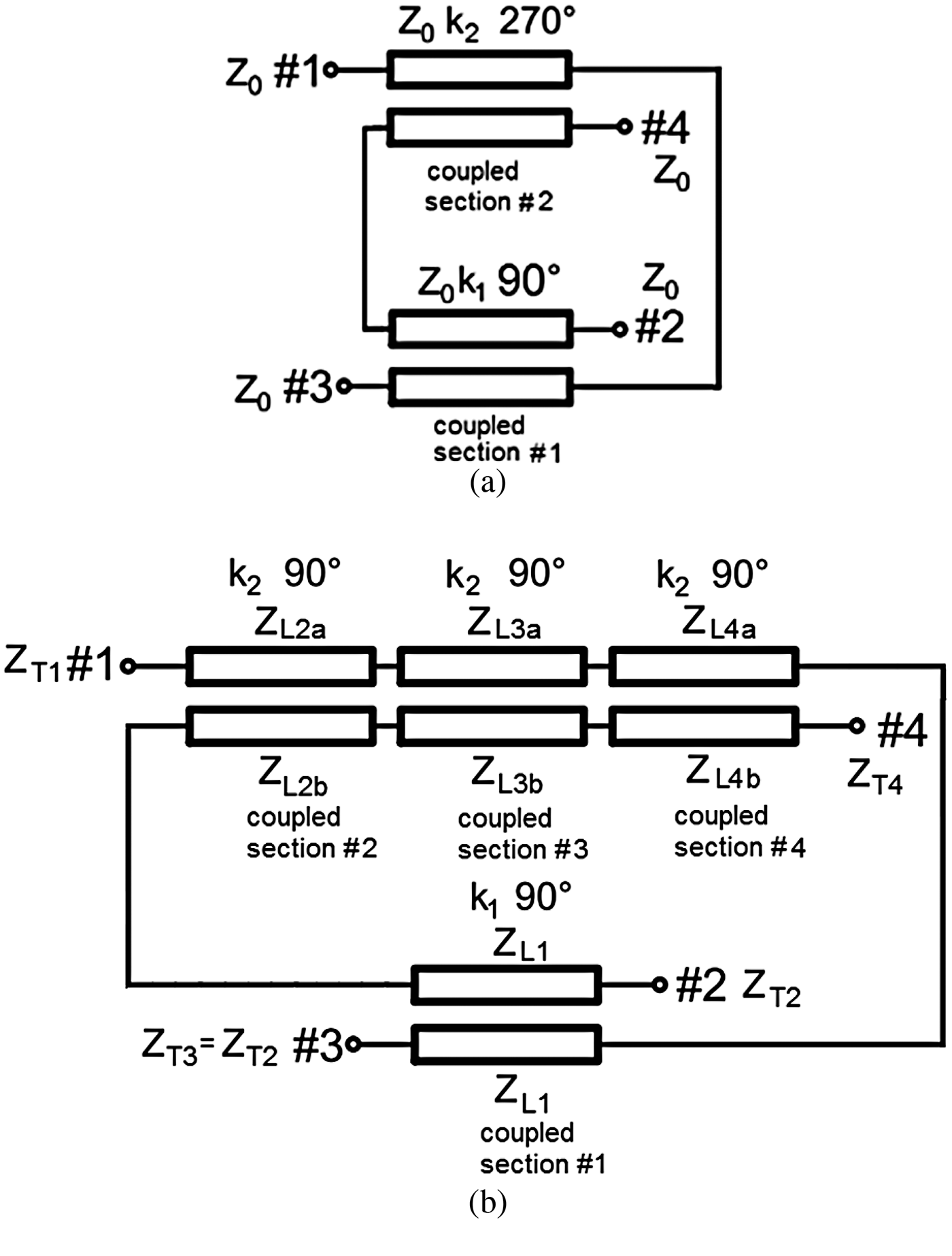
Fig. 1. Schematic diagram of a broadband directional coupler composed of two sections of unequal length [Reference Staszek, Wincza and Gruszczynski16] (a) and its modified version constituting a broadband impedance transforming directional coupler with high impedance transformation ratio (b).
Following the idea of impedance transforming directional couplers presented in [Reference Wincza and Gruszczynski13], a new type of directional couplers can be proposed as shown in Fig. 1(b). The proposed coupler originates from the one shown in Fig. 1(a) in which the three-quarter-wave-long section has been divided into three separate quarter-wave-long sections, each having the same coupling coefficient k 2 but different self-impedances of the coupled conductors, defined as
 $$Z_{La,b} = \sqrt {\displaystyle{{L_{a,b}} \over {C_{a,b}}}}, $$
where L a, b , C a, b are, respectively, the self-inductances and self-capacitances per unit length of lines a and b in the presence of the other line [Reference Sachse19]. In the proposed coupler, sections #2, #3, and #4 are used to transform the terminating impedance Z T1 to the desired value Z T2. Since three different sections are available, the obtained return losses are equivalent to the three-section quarter-wave impedance transformers [Reference Matthaei, Young and Jones20], when appropriate characteristic impedances Z L2a,b , Z L3a,b , and Z L4a,b are chosen for each line of each coupled-line section. The remaining coupled-line section #1 operates at the assumed output impedance level Z T2 with coupling coefficient k 1. The exemplary maximum transformation ratios R max and transformation ratios R for which the in-band return losses of the resulting 3-dB directional coupler are equal 20 dB are listed in Table 1 together with the coupling coefficients and coupling imbalance. One can notice that the proposed couplers allow for achieving very high transformation ratios; however, they are limited when the operational bandwidth and the required in-band return losses are assumed. Assuming that the in-band return losses are not worse than 20 dB and the entire amplitude bandwidth of the coupler is utilized the transformation ratio as high as R = 4.5 can be obtained.
Table 1. Coupling coefficients, corresponding bandwidth, maximum impedance transformation ration R max , and the transformation ration R for which in-band RL equals 20, 15, and 10 dB, for the proposed 3-dB impedance transforming directional couplers

To illustrate the behavior of the proposed couplers the frequency response of an exemplary 3-dB impedance transforming directional coupler having coupling imbalance equal 0.1 dB and R = 4.6 are presented in Fig. 2. The presented frequency response has been calculated assuming ideal asymmetric coupled-line sections and in-band return losses equal 20 dB in the operational bandwidth equal f u /f l = 2.8. The parameters of the coupled-line sections and terminating impedances are listed in Table 2. It is worth noticing that the in-band differential phase is nearly ideally equal 90°, with the error in the presented case well below 0.1 Ω.

Fig. 2. Calculated frequency characteristics of an exemplary impedance transforming 3-dB directional coupler having in-band return losses not worse than 20 dB and impedance transformation ratio equal 4.6. Coupled line sections’ parameters and terminating impedances are listed in Table 2. Amplitude – solid lines and differential phase – dashed line.
Table 2. Coupled-line sections’ coupling coefficients, self-impedances, and terminating impedances of an exemplary 3-dB impedance transforming directional coupler having in-band return losses equal 20 dB and R = 4.6.

As it is seen, the designed directional coupler features proper equal-ripple coupling and transmission characteristics. Moreover, the in-band return losses have also an equal-ripple character and are not worse than the assumed 20 dB. Also the bandwidth in terms of the return losses is identical to the bandwidth of transmission-coupling characteristics.
Similarly any transformation level from the range of R = 1–113.2 can be obtained with the exception that the operational bandwidth is not independent from R and the larger R the narrower bandwidth or the worse in-band return losses. The coupled-line self-impedances corresponding to the couplers listed in Table 1 have been listed in Tables 3–5 allowing one for a rapid design. Since the usage of self-impedance values can be difficult with standard CAD software such as e.g., AWR Microwave Office (such models are not implemented), appropriate formulas (4)–(9) have been listed in Appendix I. The presented formulas allow for calculation of per-unit-length self-capacitance and self-inductance matrices for coupled-line sections having known their coupling coefficients k and self-impedances of each coupled line. The calculated per-unit-length self-capacitance and self-inductance matrices can be directly used in CAD software, where models of such coupled lines are implemented (e.g. RLGC_CTx model in AWR Microwave Office).
Table 3. Coupled-line sections’ coupling coefficients, self-impedances, and terminating impedances of 3-dB impedance transforming directional couplers having in-band return losses equal 20 dB and Z T1 = 50 Ω.

Table 4. Coupled-line sections’ coupling coefficients, self-impedances, and terminating impedances of 3-dB impedance transforming directional couplers having in-band return losses equal 15 dB and Z T1 = 50 Ω.

Table 5. Coupled-line sections’ coupling coefficients, self-impedances, and terminating impedances of 3-dB impedance transforming directional couplers having in-band return losses equal 10 dB and Z T1 = 50 Ω.

III. EXPERIMENTAL RESULTS
Following the described in the previous section concept of broadband impedance transforming directional couplers a 3-dB directional coupler has been designed for which coupling imbalance equal 0.15 dB, R = 5, and RL = 20 dB have been chosen. The parameters of coupled-line sections have been listed in Table 6. The calculated frequency responses of the coupler are presented in Fig. 3. The coupler has been designed in a dielectric structure shown in Fig. 4 consisting of a thin dielectric layer having h 2 = 0.15 mm on which the traces of the coupler’ coupled-line sections have been etched, covered from both sides by thick dielectric layers h 1 = h 3 = 1.52 mm. The chosen structure is dielectrically homogeneous with dielectric constant ε r = 3.38. The dimensions of coupled conductors have been calculated with Linpar software [Reference Djordjevic, Bazdar, Sarkar and Harrington21] for each coupled-line section having known its coupling coefficient and self-impedances. The results of calculations are listed in Table 7. The designed impedance-transforming directional coupler has been analyzed electromagnetically in AWR Microwave Office software (EMSight module), which utilizes method of moments solver that solves for the currents on conductors embedded in a stackup of dielectric layers. The calculated frequency responses are presented in Fig. 5. The obtained responses correspond to the theoretical ones, i.e. the ripple level of transmission and coupling characteristics does not exceed ±0.2 dB and the bandwidth of the designed coupler is in full agreement to the theoretical one. The discrepancies are seen in return loss responses, which are deteriorated mainly due to the large influences of the transition regions between coupled-line sections. Figure 6 presents the layout of the designed directional coupler and as it is seen the coupled-line sections differ in widths significantly, which influences the electrical behavior of the circuit, in particular degrades the achieved return losses.

Fig. 3. Frequency characteristics the designed impedance transforming 3-dB directional coupler having in-band return losses not worse than 20 dB and impedance transformation ratio R equal 5. Coupled line sections’ parameters and terminating impedances are listed in Table 6.

Fig. 4. Cross-sectional view of the stripline coupled lines used for the design of a broadband 3-dB impedance transforming directional coupler.

Fig. 5. Frequency characteristics of the designed impedance transforming 3-dB directional coupler having in-band return losses not worse than 20 dB and impedance transformation ratio R equal 5. Results of electromagnetic calculations.

Fig. 6. Layout of the designed impedance transforming 3-dB directional coupler in which traces etched on both sides of thin dielectric layer are shown.
Table 6. Coupled-line sections’ coupling coefficients, self-impedances, and terminating impedances of 3-dB impedance transforming directional couplers having in-band return losses equal 20 dB and R = 4.6.

Table 7. Dimensions of coupled-line sections of the designed 3-dB impedance transforming directional coupler having in-band return losses equal 20 dB and R = 5.

The designed directional coupler has been manufactured and measured in a 50-Ω impedance measurement system, and the results have been recalculated to the desired impedance values of 10 Ω with respect to the ports #2 and #3. The measured frequency responses are presented in Fig. 7. The obtained results correspond to the ones obtained from electromagnetic calculations. The coupling and transmission characteristics agree well with the theoretical ones in terms of bandwidth and amplitude ripple, which is slightly larger and reaches 0.35 dB. The differential phase equals 90°, as expected, with the in-band error not exceeding 8°. The return losses are degraded due to the transition regions of the coupled-line sections and also due to the transitions between SubMiniature version A connectors and low-impedance 10 Ω lines. Nevertheless, the obtained results fully prove the proposed concept of broadband 3-dB impedance transforming directional couplers’ design. The total losses of two such couplers in a back-to-back connection equal 1.3 dB at the center frequency, hence the losses of a single coupler are on the level of 0.65 dB. Figure 8 shows a photograph of the fabricated model with top cover removed. The performance of the proposed directional coupler has been compared in Table 8 to other recently published directional couplers, which transform the impedance to the coupled and direct ports. From the comparison it is clearly seen that the proposed technique allows for realization of high transformation ratio R in wide operational bandwidth. In contrast, in the previously published couplers either the bandwidth is limited by the chosen technique for high R realization [Reference Sorocki, Piekarz, Wincza and Gruszczynski12], or the transformation ratio R is limited by the bandwidth enhancement [Reference Wincza, Piekarz and Gruszczynski15].

Fig. 7. Measured frequency characteristics of the designed impedance transforming 3-dB directional coupler having in-band return losses not worse than 20 dB and impedance transformation ratio R equal 5. Amplitude – solid lines and differential phase – dashed line.

Fig. 8. Photograph of the fabricated impedance transforming 3-dB directional coupler (with top cover removed) in which traces etched on both sides of thin dielectric layer are visible.
Table 8. Performance comparison of the proposed directional coupler with couplers presented in literatures.

IV. CONCLUSION
In this paper, a new class 3-dB impedance transforming directional couplers has been proposed. It has been shown that by taking advantage of the recently proposed directional couplers having coupled-line sections with different electrical lengths, the limitation on the achievable impedance transformation ratio R = 2 (for 3-dB couplers) can be overcome, and can reach values as high as 113. Thus one can transform an impedance in a single device from 50 to 0.44 Ω. The theoretical analysis of the proposed 3-dB couplers has been presented and confirmed by the design of a broadband 3-dB impedance transforming directional coupler operating in the frequency range of 0.5–1.5 GHz in which the impedance transformation ratio R = 5 has been achieved. The measured frequency responses support the presented theory and confirm the possibility of the proposed directional couplers’ design, which are primarily intended for application in high-power RF amplifiers. Moreover, useful tables have been given for directional couplers having in-band return losses equal 20, 15, and 10 dB and different coupling characteristics’ ripple level, for which the self-impedances of coupled-line sections are given, allowing for convenient design.
ACKNOWLEDGEMENTS
This work was partially supported by the Ministry of Science and Higher Education under Iuventus Plus program 2015-2016, contract no. 0510/IP2/2015/73 and in part by statutory activity of the Department of Electronics.
 Krzysztof Wincza received the M.Sc. degree and the Ph.D. degree in Electronics and Electrical Engineering from the Wroclaw University of Technology, Poland, in 2003 and 2007, respectively. In 2007, he joined the Institute of Telecommunications, Teleinformatics and Acoustics, Wroclaw University of Technology. In 2009, he joined the Faculty of Electronics at AGH University of Science and Technology becoming an Assistant Professor. Dr. Wincza was the recipient of The Youth Award presented at the 10th National Symposium of Radio Sciences (URSI) and the Young Scientist Grant awarded by the Foundation for Polish Science in 2001 and 2008, respectively. He has co-authored more than 40 journal and more than 50 conference scientific papers.
 Slawomir Gruszczynski received the M.Sc. and Ph.D. degrees in Electronics and Electrical Engineering from the Wroclaw University of Technology, Poland, in 2001 and 2006, respectively. Since 2001–2006 he has been with Telecommunications Research Institute, Wroclaw Division. From 2005 to 2009, he worked at the Institute of Telecommunications, Teleinformatics and Acoustics, Wroclaw University of Technology. In 2009, he joined the Faculty of Informatics, Electronics and Telecommunications at AGH University of Science and Technology where he became a Head of the Department of Electronics in 2012. He has co-authored more than 40 journal and more than 50 conference scientific papers. He is a member of the IEEE, and a member of Young Scientists’ Academy at Polish Academy of Sciences (PAN) and Committee of Electronics and Telecommunications at Polish Academy of Sciences (PAN).
APPENDIX
Typically models of coupled-line sections implemented in commercially available CAD software (such as, e.g., AWR Microwave Office) do not allow for defining asymmetric coupled-line sections with lines’ self-impedances. Instead general models are available in which the coupled-line sections are described by the elements of per-unit-length capacitance and inductance matrices, i.e. C 11, C 22, C m, L 11, L 22, and L m , respectively (e.g. RLGC_CTx model in AWR Microwave Office). Therefore, for completeness we present below the formulas, that allow for calculation of the per-unit-length matrix elements from given in the paper self-impedances ZLa,b and coupling coefficients k. These expressions take the following form:
 $$C_{11} = \displaystyle{1 \over {v(Z_{La}\sqrt {1 - k^2} )}},$$
 $$C_{22} = \displaystyle{1 \over {v(Z_{Lb}\sqrt {1 - k^2} )}},$$
 $$C_m = \displaystyle{k \over {v\left( {\sqrt {Z_{La}Z_{Lb}(1 - k^2)}} \right)}},$$
 $$L_{11} = \displaystyle{{C_{22}} \over {v^2(C_{11}C_{22} - C_m^2 )}},$$
 $$L_{22} = \displaystyle{{C_{11}} \over {v^2(C_{11}C_{22} - C_m^2 )}},$$
 $$L_m = \displaystyle{{C_m} \over {v^2(C_{11}C_{22} - C_m^2 )}},$$
where v is the speed of light in a free space.


