Introduction
Antennas with omni-directional linear polarized, dual polarized, and circularly polarized (CP) radiation pattern are widely used [Reference Park and Lee1–Reference Dai, Wang, Liang, Chen and Wang14]. On one hand, the omni-directional radiation pattern makes the wireless devices accessed easily. On the other hand, the CP electromagnetic wave can decrease the reflections formed by multi-path. So, the omni-directional CP antenna is suitable for wireless communication systems.
Various omni-directional CP antennas have been researched in past few years. In [Reference Park and Lee1], the omni-directional CP meta-material antenna is proposed. The ZOR (Zeroth Order Resonance) mode of epsilon negative transmission line is used to get an omni-directional vertical polarization and the curved branches are used to get an omni-directional horizontal polarization. The literature in [Reference Yu, Gong, Wan, Yao, Xu and Wang2,Reference Pan, Zheng and Hu3] utlizes the multimode TM 01 and TM 02 of the circular patch to generated wideband omni-directional CP characteristics. By coupling the TM 01 and the TM 02 modes of the circular patch, a wideband property is achieved. A new omni-directional CP antenna is proposed in [Reference Li, Liao and Xue4], the current loop formed by the printed spoke-like metal strips fabricated on two substrates and the monopole is formed by a metal sleeve. The antenna exhibits an omni-directional CP radiation in azimuthal plane. Besides, dual-band omni-directional CP antennas [Reference Yu, Gong, Wan and Chen5], omni-directional CP dielectric resonator antennas [Reference Li and Leung6], and reconfigurable omni-directional CP antennas [Reference Cai, Gao, Yin, Li and Luo9] have also attracted much attention.
However, less work has been done on high-gain omni-directional CP antenna. A novel design of omni-directional CP antenna array has been proposed in [Reference Shi, Wu, Qing and Chen8]. The antenna element consists of an electric dipole and a zero-phase-shift (ZPS) line loop. Such a configuration makes the antenna obtain higher gain. However, the feed point in [Reference Shi, Wu, Qing and Chen8] is placed in the middle of the substrate. The coaxial cable connecting with the antenna will affect the omni-directional property, which leaves the antenna not suitable for practical use.
In this paper, a bottom feed omni-directional CP antenna array is presented. The antenna array consists of four elements. Two dipoles provide E θ component while two ZPS line loops provide E φ component. Four elements are fed in the same phase and amplitude by T-shaped parallel strip line power divider. As a result, omni-directional CP radiation is achieved in the far field of the proposed antenna. The feeding point is placed at the bottom of the antenna. The structure which transferred parallel strip line to microstrip line is used to eliminate the unbalanced current of the coaxial cable. This structure makes the antenna array more suitable for practical use. The antenna achieves the impedance bandwidth of 0.13 GHz (2.40–2.53 GHz) and the omni-directional CP property is stable over WLAN bands. The measured maximum CP gain is 4.8 dBic. The antenna structure, working principle, simulated and measured results are presented as follows.
Proposed antenna design
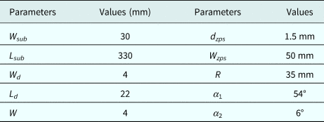
The configuration of the proposed omni-directional CP antenna array is shown in Fig. 1. The antenna array consists of a vertical substrate and two horizontal substrates. Two horizontal substrates are vertically assembled into the two sides of the vertical substrate, respectively. The parallel strip-line feeding network and the dipoles is printed on the vertical substrate while the two ZPS line loops are printed on horizontal substrates. All the substrates are 2.65 in dielectric constant and 1 mm in height. The antenna is a four-element array and the array contains two dipoles and two ZPS line loops. The antenna is vertically placed. The parallel strip line feeding network with a balanced structure is used in the bottom of the antenna. The overall size of the antenna is 50 mm × 30 mm × 330 mm. The geometry of the antenna is shown in Fig. 1, where the front and back views are presented. P is the feeding point of the antenna which can be implemented by coaxial cable.

Fig. 1. The configuration of proposed antenna. (a) Front view (b) Back view.
The design principle of an omni-directional CP antenna is to use an electric monopole and a magnetic monopole. When the electric monopole and the magnetic monopole are fed with the same current, the far field can be divided into two orthogonal components with 90° difference in phase. By adjusting the amplitude of each component, omni-directional radiation pattern can be obtained. In this letter, the dipoles are similar to electric monopoles and the current loops are similar to magnetic monopoles. The printed half-wavelength dipoles provide E θ component while the ZPS line loop provide E φ component. The ZPS lines used in this paper have been reported in [Reference Wei, Zhang, Feng and Iskander10]. The proposed structure in [Reference Wei, Zhang, Feng and Iskander10] is composed of several parallel-plate transmission line sections with periodically gap loaded. The periodical gap length is d zps. The resonance frequency of ZPS line loop can be adjusted by the width of the transmission line and the length of the gaps between each section. According to [Reference Wei, Zhang, Feng and Iskander10], the resonance characteristics are listed with detailed equations. The periodically loaded parallel-plate line can be seen as an open-ended or short-ended resonator. The resonant frequency is independent of the length of the resonator but depends only on the reactive loadings. That is to say, the resonant frequency can be decided by the related parameters α1 and α2 of the periodically loaded parallel-plate lines. Figure 2(a) shows the geometry of the ZPS line loop. The proper values of parameters of ZPS line loop are chosen to make the ZPS line loop work at 2.45 GHz. Figure 2(b) shows the current distribution at 2.45 GHz. The feeding point P of the ZPS line loop is connected with the parallel strip line feeding network. The current distribution shows that the ZPS line loop is resonant at 2.45 GHz while the phases along the current loop are coincident. The detailed values of parameters are listed in Table 1.

Fig. 2. The configuration of the ZPS line loop in [Reference Wei, Zhang, Feng and Iskander10]. (a) The geometry of the ZPS line loop. (b) The current distribution at 2.45 GHz.

The dipoles and the ZPS line loops are fed in the same phase and amplitude to ensure the omni-directional CP radiation and the maximum radiation towards azimuthal plane. To make the phase of each element identical, the distance of each element in z-axis direction should be one wavelength in the substrate (λg). The feeding network is composed of one input port and four output ports. The elements are fed with the same amplitude and phase. λg/4 impedance transformers are used in a network to get proper power ratio(1:1:1:1). The detailed values of marked impedance in Fig. 3 are listed in Table 2. The impedance of the transmission line can be calculated as:
 $$\eqalign{& Z_0 = 50\Omega \cr & Z_{\,pot1} = Z_{\,pot2} = Z_{\,pot3} = Z_{\,pot4} = 50\Omega \cr & Z_{in1} = Z_{\,pot1}/3 = 16.67\Omega \cr & {{Z}^{\prime}}_{in1} = \lpar {Z_{in1}\cdot Z_{\,pot1}} \rpar /\lpar {Z_{in1} + Z_{\,pot1}} \rpar = 12.5\Omega \cr & {{Z}^{\prime}}_{in1}\cdot Z_0 = Z_5^{2} \cr & Z_5 = 25\Omega \cr & Z_{in1}\cdot Z_0 = Z_4^2 \cr & Z_4 = 28.86\Omega \cr & Z_{in2} = Z_{\,pot2}/2 = 25\Omega \cr & {{Z}^{\prime}}_{in2} = \lpar {Z_{in2}\cdot Z_{\,pot2}} \rpar /\lpar {Z_{in2} + Z_{\,pot2}} \rpar = 16.67\Omega \cr & {{Z}^{\prime}}_{in2}\cdot Z_0 = Z_3^2 \cr & Z_3 = 28.86\Omega \cr & Z_{in2} \bullet Z_0 = Z_2^2 \cr & Z_2 = 35.35\Omega \cr & Z_{in3} = Z_{\,pot4} = 50\Omega \cr & {{Z}^{\prime}}_{in3} = \lpar {Z_{in3}\cdot Z_{\,pot3}} \rpar /\lpar {Z_{in3} + Z_{\,pot3}} \rpar = 25\Omega \cr & {{Z}^{\prime}}_{in3}\cdot Z_0 = Z_1^2 \cr & Z_1 = 35.35\Omega} $$
Fig. 3. The impedance of the proposed antenna.
Table 2. Detailed values of marked impedance in Fig. 3.

It should be mentioned that the ZPS line loops are inserted at both sides of the vertical substrate. The 180° (λg/2) phase delay parallel strip line is used in the upper ZPS line loops to ensure the current on two current loops are same to each other in direction. Two dipoles are also printed at a different side of the substrate. In this way, the antenna array can obtain a better omni-directional property.
The structure which transfers parallel strip line to microstrip line is used in the bottom of the network to eliminate the unbalanced current of the coaxial cable. In the already published papers, the feeding points of the omni-directional CP antenna array are placed in the middle of the whole antenna. Compared with the former types, the coaxial cable which connects to the feeding point almost has no influence on the omni-directional property of the proposed antenna. The antenna is more suitable for practical use. In addition, the transfer structure has less effect on the high-gain property.
Simulated and measured results
The proposed antenna is simulated by HFSS. The antenna is fabricated on FR4 substrate with a relative dielectric constant of 2.65 and a dielectric loss of 0.002. Figure 3 presents the current distribution of the proposed antenna, the current direction of two dipoles are identical at 2.45 GHz, and so do the two ZPS. As shown in Fig. 4, the proposed antenna element generates the left-hand CP (LHCP) radiation when the ports are fed in-phase. The right-hand CP (RHCP) radiation can be generated by exchanging the positive/negative parts of the feeding point of the ZPS line loop to reverse the flowing direction of the current along the ZPS line loop. Figure 5 shows the prototype of the antenna.

Fig. 4. The current distribution of the proposed antenna (a) dipole (b) ZPS.

Fig. 5. The fabrication of the proposed antenna array. (a) Front view (b) Back view.
The S-parameters of the antenna are measured by Anritsu 37269A vector network analyzer. The simulated and measured |S11| curve is shown in Fig. 6. The measured results are essentially in agreement with the simulated data. The bandwidth of |S 11| <−10 dB is 0.13 GHz (2.40–2.53 GHz).

Fig. 6. The simulated and measured |S 11| of the proposed antenna.
The radiation patterns of the antenna are obtained by measuring two orthogonal linear polarization. Figure 7 shows the radiation patterns in the xoy (θ = 90°) and the yoz (φ = 90°) planes at 2.45 GHz. In the xoy plane, LHCP is the co-polarization. The measured amplitude of LHCP fields is at least 17 dB stronger than the amplitude of RHCP fields. The radiation pattern is generated in xoy plane. The roundness of the omni-directional radiation pattern is <1.39dBic. In x direction (yoz plane (φ = 90°)), the maximum radiation is in azimuthal plane and desired ARs are obtained in azimuthal plane. The amplitude of LHCP fields is at least 20 dB higher than the amplitude of RHCP fields at 2.45 GHz in azimuthal plane. The simulated results also present the stability of the radiation patterns over the WLAN band (2.412–2.472 GHz).

Fig. 7. The simulated and measured radiation patterns of the proposed antenna at 2.45 GHz. (a) xoy plane (θ = 90°) (b) yoz plane (φ = 90°).
Figure 8 shows the simulated and measured ARs in the xoy (θ = 90°) plane. From Fig. 8, the measured and simulated ARs in the xoy plane are all <3 dB which indicate a good CP property. The difference between the measurement and the simulation is due to the imperfect fabrication of the antenna and the effects of the measuring environment. Besides, the measured maximum gain is 4.8 dBic in azimuthal plane, which is much lager than omni-directional CP antenna unit, whose gain is usually no more than 2.5 dBic. The simulated radiation efficiency is 93% at 2.45 GHz.

Fig. 8. The measured and simulated ARs at 2.45 GHz in the xoy plane of the proposed antenna.
The antenna array consists of two dipoles and two ZPS line loops. A 1–4 T-shaped parallel strip line feeding network is used to connect the elements and a 180° phase delay parallel strip line is used to ensure the current on ZPS line loops are in the same direction. Such a configuration guarantee that the antenna array obtains a high gain property and the maximum direction towards the azimuthal plane.
Moreover, the structure which transferred parallel strip line to microstrip line is used in this antenna. Compared with other high-gain omni-directional CP antenna array, this structure can eliminate the unbalanced current of the coaxial cable. Besides, the feed point is placed in the bottom of the antenna so that the effects on omni-directional property brought by the connecting coaxial cable decreases.
Conclusion
A bottom-feed omni-directional CP antenna array is presented in this paper. The antenna array consists of two dipoles and two ZPS line loops, which are connected by T-shaped parallel strip line feeding network and the antenna array utlizes bottom-feed way to improve the omni-directional property. As a result, the impedance bandwidth of the proposed antenna is 0.13 GHz and high gain of 4.8 dBic can be achieved. The antenna can be a good candidiate for wireless communication which requires high-gain omni-directional CP antenna.
 Xi Li was born in Shanxi, China, in 1983. He received the B.S., and Ph.D. degrees in electromagnetic field and microwave technology from Xidian University, Xi'an, China, in 2006, and 2011, respectively. In 2011, he joined the National Laboratory of Science and Technology on Antennas and Microwaves, Xidian University, as an Associate Professor. He has authored or co-authored over 40 referred journal and conference papers. His current research interests include the design of antenna, electromagnetic analysis, and antenna measurement method research.
 Lin Yang was born in Weinan, Shaanxi Province, China. He received the M.S. degree in electromagnetic fields and microwave technology from Xidian University, Xi'an, China in 1983. Lin Yang worked at the Institute from 1983 to 2003. Since 2003, he has worked at Xidian University and is currently a professor with the National Key Laboratory of Antennas and Microwave Technology at Xidian University. His research interests include antenna theory and engineering design.