


Introduction
Rapid development in the field of radar and communication systems leads to growing attention in the design of microwave absorbers. Generally, the reflection of incident electromagnetic wave is inhibited by random metallic structures arranged periodically/non-periodically above metal-backed dielectrics. The classical absorbers such as Salisbury screen consists of resistive sheets placed a quarter wavelength apart from the metallic back plane [Reference Roland1]. However, it suffers from larger structural height due to quarter wavelength spacing. Frequency selective surfaces (FSSs) are introduced in the design of microwave absorbers to obtain wider bandwidth with reduced substrate thickness [Reference Seman, Cahill, Fusco and Goussetis2]. Over the past few decades several studies have been carried out on multi-band, polarization insensitive, and broadband microwave absorbers for potential applications in radar cross-section reduction, sensors, energy harvesting from microwaves and many more [Reference Roland1–Reference Dincer, Akgol, Karaaslan, Unal and Sabah3]. The authors' of previous work proposed a compact broadband absorber with a single layer metal grounded substrate and an array of patch FSS on the top plane for X and Ku band applications [Reference Sen, Kumar, Islam and Das4]. But the challenge remains in the design for bi-directional applications with dual bandwidth operability. A new type of FSS called absorptive FSS (AFSS) is first introduced in 1995 [Reference Arceneaux, Akins and May5]. AFSS with broadband absorption at low frequency and in-band transmission at high frequency based on parallel resonance is reported in [Reference Chen, Liu, Chen, Bai and Fu6]. AFSS with a transmissive property at upper frequency band using parallel LC resonance is also proposed by Chen et al. [Reference Chen, Yang, Bai and Fu7]. Recently AFSS with bi-directional absorption has gained attentions due to its versatile application. A dual directional absorber is first introduced in 2010 [Reference Gu, Barrett, Hand, Popa and Cummer8]. Later, Ayop et al. [Reference Ayop, Rahim and Murad9] have proposed a dual directional AFSS for diverse applications in the X band.
In this work, a bi-directional dual bandwidth microwave absorber is designed using multilayer compact FSS structures. The wideband response is obtained by multiple resonances occurring at the top plane due to staircase design of the patch. Whereas, the waves coming from the opposite side sees a single resonating structure and gives a narrowband response.
Bi-directional absorber design
Figure 1 shows the unit cell of the proposed bi-directional dual bandwidth absorber (BDDBA). It comprises three metallic layers with dielectric materials (with heights h 1 and h 2) sandwiched in between them (Fig. 1(a)). The top layer consists of a staircase metallic patch as shown in Fig. 1(b). The middle and bottom metal layers are composed of an array of identical four (2 × 2) meander square loop patches and given in Fig. 1(c). Dielectric material is chosen as an FR4-Epoxy substrate having a permittivity of 4.4, dielectric loss tangent = 0.02. The dimensions of the proposed design are tabulated in Table 1.
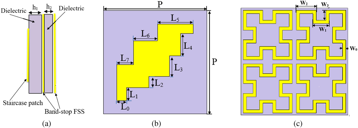
Fig. 1. Unit cell of the proposed BDDBA: (a) side view, (b) top view, and (c) bottom view.
Table 1. Unit cell dimensions in “mm”.

Results and discussion
The absorptivity of the proposed absorber can be calculated [Reference Landy, Sajuyigbe, Mock, Smith and Padilla10] as,
 $$A\,(\omega )\, = \,1\,-\,T\,(\omega )\,-\,R\,(\omega )$$
where A(ω), T(ω), and R(ω) are the absorptivity, transmissivity, and reflectivity. The maximum absorption can be achieved when both transmission (T(ω) = |S 21|2) and reflection (R(ω) = |S 11|2) become minimum, where S 11 and S 21 are the reflection and transmission coefficients.
The structure of the presented bi-directional microwave absorber is simulated with unit cell boundary conditions using simulation software CST Microwave Studio. Figures 2(a) and 2(c) depict the setup of the absorber with the direction of incident wave and the corresponding wideband and narrowband responses are shown in Figs 2(b) and 2(d). The relative absorption bandwidth (RAB) of 39.40% covering from 10.20 to 15.20 GHz with more than 90% absorption achieved when an electromagnetic wave impinges normally on the top plane (from positive Z direction in Fig. 2(a)) making it suitable for broadband applications in the X and Ku bands. For the wave incident normally on the bottom plane (from negative Z direction in Fig. 2(b)), the same structure gives narrow band absorption with an RAB of 2.29% (260 MHz) with more than 90% absorption around 11 GHz.
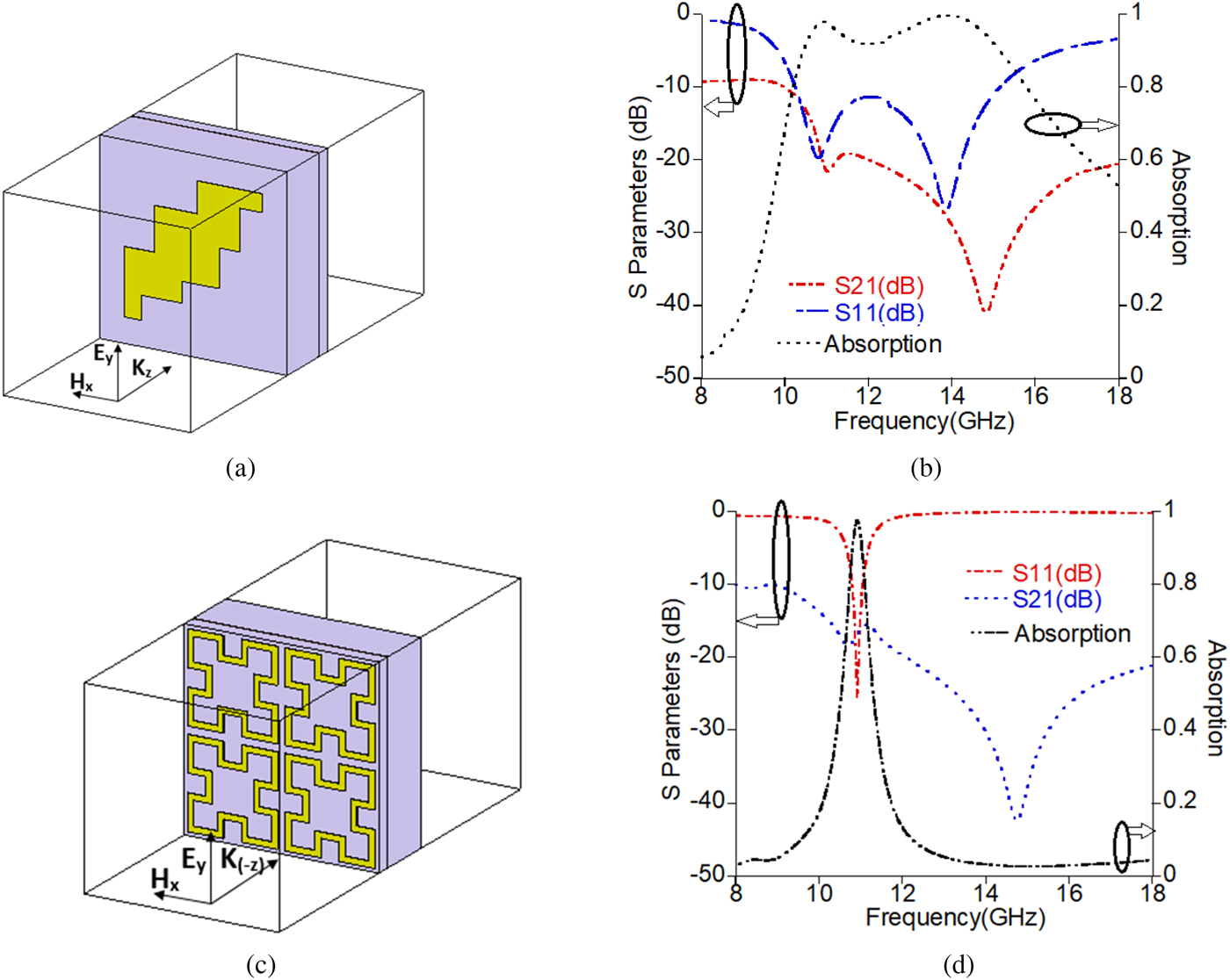
Fig. 2. Simulated responses of the absorber with the direction of the incident wave: (a) setup for wideband absorption, (b) wideband response, (c) setup for narrowband absorption, and (d) narrowband absorption result.
The effective surface impedance of the absorber as seen on the interfaces can be represented in terms of S parameters as,
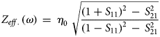 $$Z_{eff.}\,(\omega )\, = \,\eta _{0\;} \,\sqrt {\displaystyle{{{(1 + S_{11})}^2\,-\,S_{21}^2} \over {{(1-S_{11})}^2\,-\,S_{21}^2}}} $$
where Z eff.(ω) and η 0 represent frequency dependent effective surface impedance and free space impedance, respectively.
Figure 3 depicts complex surface impedance (Z eff.) variations as normalized with the free space impedance (η 0) of the proposed absorber. Figure 3(a) shows that the real part (Z_real) of the Z_eff is near to unity and the imaginary component (Z_img) is near to zero within 10.20–15.20 GHz. Therefore, a wideband absorption occurs due to matching of the surface impedance of the absorber with free space. The same phenomena occur for narrowband absorption around the frequency of 11 GHz and is shown in Fig. 3(b).
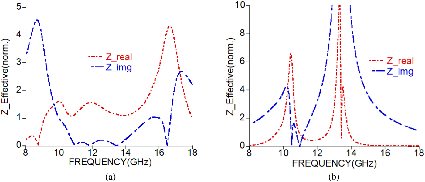
Fig. 3. Effective normalized surface impedance ( $Z_{eff.\_norm}$) variations of the proposed absorber with frequency for (a) wideband and (b) narrowband response.
The absorption performance is also analyzed for different angles (θ) of the incident wave in both directions and is shown in Fig. 4. A wideband response with more than 80% absorption is observed at different angles (θ) from 0 to 45° (Fig. 4(a)) and hence makes the structure incident angle independent within that range. Increase in angle “θ” results in the absorption response at higher band is slightly deteriorated due to higher order modes while at the first resonant peak it remains unchanged. The narrowband performance of the design remains unaltered with the change in incident angle “θ” due to symmetric nature of the bottom FSS layers as is evident in Fig. 4(b).
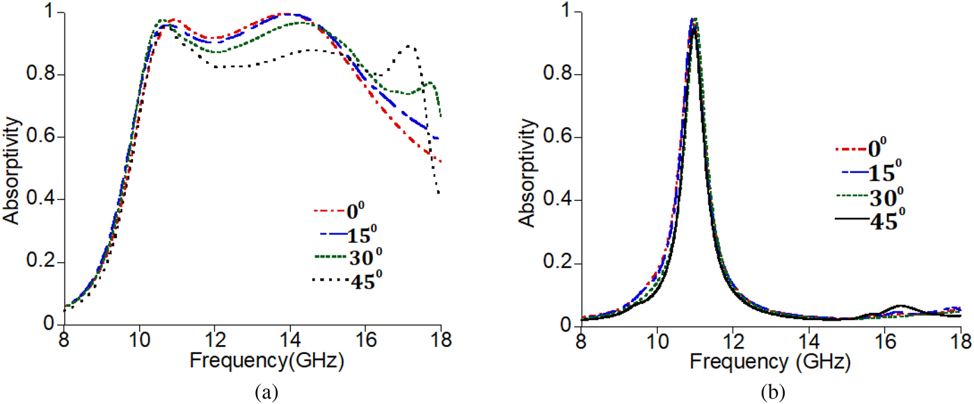
Fig. 4. The absorption performance for different oblique incident angles (θ): (a) wideband response and (b) narrowband response.
The physics behind dual bandwidth absorption is well understood by studying the surface current distributions. The surface current density is analyzed at an absorption frequency of 11 GHz on the top, middle and bottom metal layers of the proposed design and is given in Fig. 5. Figure 5(a) depicts the surface currents on the top layer oriented diagonally having maximum path length. This is due to strong electric resonance at the patch. The surface current paths on each of the resonator of the middle and bottom FSS layers (Figs 5(b) and 5(c)) are antiparallel (shown with an arrow). This is because of strong magnetic coupling existing between them. As a result, absorption occurs due to combination of both electric and magnetic resonances in the three layers. At the higher frequency of 14 GHz the strong presence of surface current is observed only at the top layer and rest of the FSS layers are having negligible density (Fig. 6). The current path on the top patch follows the shortest distance diagonally at this frequency (Fig. 6(a)). From this analysis it can be concluded that wideband absorption occurs mainly due to the top layer resonator and narrowband absorption is obtained due to the middle and bottom FSS layers.
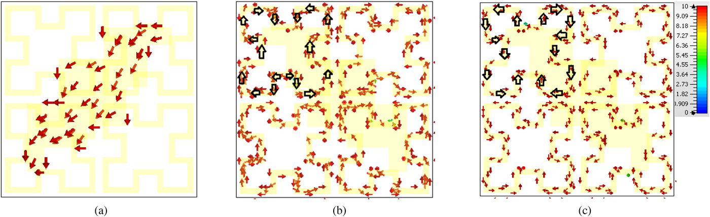
Fig. 5. Surface current distributions at the absorption frequency of 11 GHz on (a) top layer, (b) middle layer, and (c) bottom FSS layer.
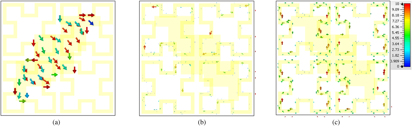
Fig. 6. Surface current distributions at 14 GHz on (a) top layer, (b) middle FSS, and (c) bottom FSS layer.
Experimental validation
A prototype of the proposed absorber structure is fabricated whose, top and identical middle and bottom FSS layers are given in Figs 7(a) and 7(b). The waveguide measurement method [Reference Bayatpur and Sarabandi11–Reference Zhai, Zhan, Li and Liang12] is carried out for experimental validation and its schematic diagram is shown in Fig. 7(c). An Agilent N5230A series vector network analyzer and a pair of waveguides, WR-90 and WR-62 operating at X and Ku bands with aperture dimensions of 23 × 10 mm2 and 15 × 9 mm2, respectively are used. The plane wave incident on the sample's interface from the waveguide at an incident angle calculated as, θ = sin−1(λ/2a) (a is the width of the aperture of waveguide, and λ is the wavelength). The proposed absorber has a stable absorption response over the wide angles of incident EM wave and thus, it makes the measurement setup effective. The scattering parameters, S 11 (dB) and S 21 (dB) are measured as reflection and transmission coefficients of the absorber for the wideband response, whereas, S 22 (dB) and S 12 (dB) are reflection and transmission coefficients of the design for the narrowband operation. The measured and simulated results are plotted in Fig. 8, which depicts the simulated results closely following the measured one.
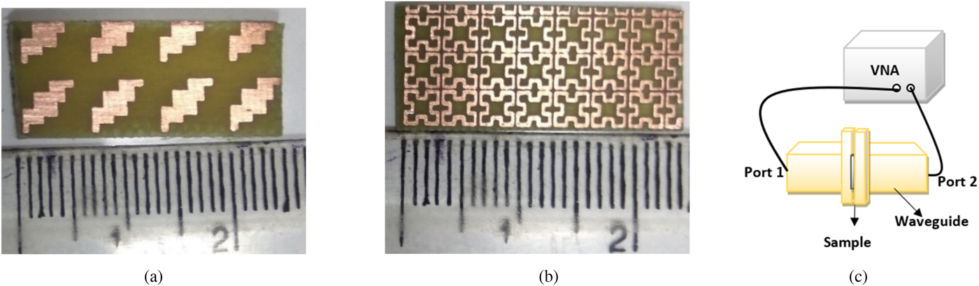
Fig. 7. (a and b) Fabricated prototype of the proposed absorber: (a) top plane, (b) identical middle and bottom plane, and (c) schematic diagram of measurement setup.
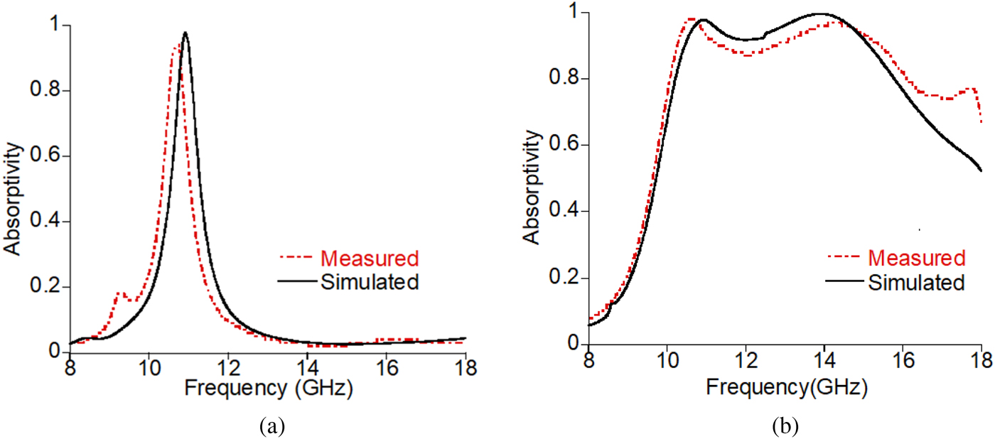
Fig. 8. Measured absorptivity response along with the simulated one: (a) wave incident from the negative Z-axis and (b) wave incident from the positive Z-axis.
Conclusion
A bi-directional dual bandwidth low profile microwave absorber is designed for X and Ku band applications. A wide absorption bandwidth of 5 GHz (RAB = 39.40%) with more than 90% absorption is obtained at normal incidence on the top staircase patch layer. A narrowband absorption bandwidth of 260 MHz (RAB = 2.29%) with more than 90% absorption is obtained for the wave impinges normally at the bottom FSS layer from the back side of the structure. A stable performance of the structure with varying incident angle is also observed. The validation of the design is performed by comparing its response with the experimental data. The design of the proposed microwave absorber is cost effective thus found to be suitable for diverse bi-directional applications.
 Gobinda Sen received his B.Tech degree in Electronics and comm. Engineering from the West Bengal University of Technology in 2010, and his M.Tech degree in Communication Engineering in 2013. He is currently pursuing his Ph.D. degree in Microwave engineering with the Electronics and Tele-Communication Engineering Department, Indian Institute of Engineering Science and Technology at Shibpur, Howrah, India. His current research interests include metamaterial inspired structure for performance improvement of antenna, frequency selective surfaces, and microwave absorbers.
 Dr. Santanu Das received his B.E. degree in Electronics and Telecom. Engineering from the Bengal Engineering College in 1989, and his M.E. degree in Microwave Engineering from Jadavpur University, Calcutta in 1992. He obtained his Ph.D. (Engineering) degree in 1998 from Jadavpur University. As a Lecturer in Electronics and Telecommunication Engineering, he joined the department of the Bengal Engineering and Science University in 1998 and presently holds the post Professor in the same department. His current research interests include the microstrip circuits, antenna elements and arrays, FSS and defected ground structures. He is a life member of the Institution of Engineers, India.


