Introduction
Many attempts have been made to overcome the low gain and narrow bandwidth of the microstrip antenna [Reference Garg, Bhartia, Bahl and Ittipiboon1]. In this process, several measures were taken such as modifying the shape of radiating elements [Reference Tarange, Gite, Musale and Khobragade2] and modifying the ground plane structure [Reference Mondal and Sarkar3], use of low dielectric constant material, stacked patch antenna, use of impedance matching networks etc. [Reference Khidre, Lee, Yang and Elsherbeni4–Reference Sung6] and creating defect in the ground plane [Reference Gautam, Bisht and Kanaujia7]. Different feeding techniques such as L-strip proximity feeding, T-shape probe feeding etc. are also used to increase the bandwidth [Reference Singh and Kumar8, Reference Mak, Lee and Luk9]. In the literature some theoretical analysis of strip line fed, L-strip/L-probe fed patch antennas have also been reported for the wideband operation [Reference Meshram10, Reference Yadav, Wu, Fang and Singh11]. When the strip line feeding is modified as L-strip/L-probe it provides better gain and directivity suitable for wideband operation and antenna array design. In such feeding an additional capacitance is created between the radiating patch and the feed which cancels the inductance of the vertical portion of the L-probe. Consequently, this effect broadens the impedance bandwidth of the antenna [Reference Singh, Gangwar and Kanaujia12].
In this paper, symmetrical slots are etched in the radiating patch and modified L-probe feeding is used to increase the antenna bandwidth. The present design gives better impedance bandwidth and gain as compared with the previously reported results [Reference Park, Na and Baik13–Reference Bilgic and Yeğin16]. The antenna parameters are calculated using high frequency structure simulator (HFSS) and verified with IE3D simulators. The proposed designs are also analyzed using circuit theory concept. The theoretical and simulated results are validated with measured results.
Antenna geometry and theoretical analysis
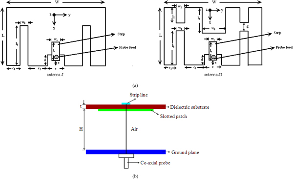
In conventional design of L-probe feeding, probe is required to bend which makes the design process complicated. But, in the present paper a narrow horizontal conducting strip is printed on the upper side of the substrate of thickness t and the radiating patch on the lower side. In order to avoid the bending procedure, a vertical thick probe is soldered to the horizontal strip. A small portion of patch is removed so that unnecessary drilling of the patch can be avoided. The present structure looks like a capacitively loaded L-probe fed patch antenna. Figure 1 shows the top view and side view of the proposed antennas. In antenna-I, two symmetrical notches of dimensions l 1 × w 1 are incorporated along one of the radiating side of the patch resulting an E-shaped structure. In antenna-II, two additional notches of dimensions l 2 × w 2 and a center notch of dimensions l 3 × w 3 are introduced in the opposite radiating edge. For the wideband operation air substrate of thickness H is used between ground plane and the patch. The design specification of the proposed antenna is presented in Table 1.

Fig. 1. Geometry of antenna (a) Top view (b) Side view for antenna-I and antenna-II.
Table 1. The design specification of the proposed antennas.

Equivalent circuit for the modified L-probe
The modified L-probe can be considered as two sections, one is vertical probe and another is horizontal strip. Lumped elements of each section contribute in the total impedance of the antennas.
Vertical probe: From Fig. 2(a), the vertical probe can be analyzed as a series combination of resistance R v and inductance L v and can be given as [Reference Bahl and Bhartia17]
 $$R_v = \displaystyle{{\sqrt {\pi {\rm f}\mu /\sigma}} \over {d_p}}(H + t),$$
where μ = permeability of the probe conductor, f = frequency in GHz, d p = diameter of probe and
 $$L_v = 2.032\lpar {h + t} \rpar \left[ {{\rm ln}\displaystyle{{\lpar {H + t} \rpar } \over {d_p}} + 0.2235\displaystyle{{d_p} \over {\lpar {H + t} \rpar }} + 1.193} \right]nH{\rm.} $$
Fig. 2. (a) Equivalent circuit of modified L-probe (b) equivalent circuit of antenna-I and (c) modified circuit of (b).
Horizontal strip: A series combination of distributive resistance R s and inductance L s is developed due to horizontal conducting strip and can be given as [Reference Hoffman18].
 $$L_s = 0.2\lpar {H + t} \rpar \left[ {{\rm ln}\left\{ {\displaystyle{{2\lpar {H + t} \rpar } \over {w_s + t_s}}} \right\} + 0.2235\left\{ {\displaystyle{{w_s + t_s} \over {\lpar {H + t} \rpar }}} \right\} + 0.5} \right]\;(nH),$$
 $$R_s = 4.13 \times 10^{-3}(H + t)\displaystyle{{\sqrt {{\rm f}\rho _0} } \over {\left( {w_s + t_s} \right)}}{\rm with}\;f\;{\rm in}\;{\rm GHz}.$$
Here, w s = width of the strip, t s = thickness of the strip, ρ 0 = ratio of the specific resistance of strip and copper.
The distributive capacitance C sp between the horizontal strip and the radiating patch can be given as:
 $$C_{sp} = \displaystyle{{\varepsilon _r\varepsilon _0l_sw_s} \over t}.$$
Since the open ends of the horizontal strip above the radiating patch will have a fringing field, the effective length of the strip is increased. The increment of length will cause some extra capacitance which is fringing capacitance and it can be calculated as:
 $$C_f = \displaystyle{{l_e\varepsilon _e^{-1/2}} \over {cZ_0}}$$
here,
 $$l_e = {\rm \;} \displaystyle{{0.412{\rm h}\lpar {\varepsilon_e + 0.3} \rpar \lpar {w_s/h + 0.264} \rpar } \over {\lpar {\varepsilon_e-0.258} \rpar \lpar {w_s/h + 0.8} \rpar }},$$
in which, ε e is the effective dielectric constant for the material under conducting strip [Reference Bahl and Bhartia17]. The fringing capacitance C fp between the open end of the strip and the patch is calculated by putting the substrate height h = t and the fringing capacitance C fg can be given by putting h = (H + t). The entire feeding acts as a series L−C resonant element and connected in series with the radiating patch.
Equivalent circuit for antenna-I and antenna-II
The antenna-I is realized by introducing two parallel slits in the radiating edge and symmetrical with respect to the horizontal strip. This radiating structure is considered equivalent to two resonators, one as an original patch and another as a modified patch with additional series inductor ΔL 1 and capacitance ΔC 1 with the initial inductance L p and capacitance C p of the origin patch. The value of ΔL 1 and ΔC 1 can be given by [Reference Zhang and Yang19, Reference Bahl20]. Now, these two resonators are coupled through the coupling capacitance C c1 (Fig. 2b) and its value can be given as:
 $$C_{c1} = \displaystyle{{-\lpar {C_p + C^{{\prime}}} \rpar + \sqrt {({(C_p + C^{{\prime}})}^2-4C_pC^{{\prime}}(1-(1/C_m^2 )))}} \over 2},$$
here,
 $$C^{{\prime}} = \displaystyle{{\Delta C_1C_p} \over {\Delta C_1 + C_p}},$$
 $$C_m = \displaystyle{1 \over {\sqrt {Q_1Q_2}}}, $$
where Q 1 and Q 2 are the quality factors of the two resonators.
The microstrip patch is considered as a parallel combination of resistance (R p), inductance (L p) and capacitance (C p) and the corresponding values are given as [Reference Hoffman18].
 $$C_p = \displaystyle{{\varepsilon _0\varepsilon _e{\rm LW}} \over {2{\rm H}}}{\rm co}{\rm s}^{-2}\left( {\displaystyle{{L_s\pi} \over L}} \right),$$
 $$L_p = \displaystyle{1 \over {\omega ^2C_p}},$$
 $$R_p = \displaystyle{{Q_r} \over {\omega C_p}}.$$
In the proposed geometry, the effective dielectric constant for the fed patch is calculated by [Reference Liu, Kooi, Li, Leong and Yeo21]:
 $$\varepsilon _e = \displaystyle{{\varepsilon _{rs} + 1} \over 2} + \displaystyle{{\varepsilon _{rs}-1} \over 2}\left( {1 + \displaystyle{{12H} \over W}} \right)^{-1/2},$$
where, “H” is the thickness between ground and slotted patch, and
 $$\varepsilon _{rs} = \displaystyle{{\mathop \sum \nolimits_{i = 1}^n h_i} \over {\mathop \sum \nolimits_{i = 1}^n \displaystyle{{h_i} \over {\varepsilon _{ri}}}}},$$
where n is the number of stacked layers.
The equivalent circuit of the modified L-probe fed antenna-I is shown in Fig. 2(b). The input impedance for this antenna can be calculated using Fig. 2(c).
 $$Z_{in} = Z_{LP} + Z^{\rm \prime\prime}, $$
where,
 $$Z_{LP} = R_v + j\omega L_v + R_s + j\omega L_s + \displaystyle{1 \over {\,j\omega C_{eq}}},$$
in which,
 $$C_{eq} = \displaystyle{{\lpar {C_{\,fg}} \rpar \lpar {2C_{\,fp} + C_{sp}} \rpar } \over {\lpar {C_{\,fg} + 2C_{\,fp} + C_{sp}} \rpar }},$$
and
 $$Z^{\rm \prime\prime} = \displaystyle{{Z_EZ^{{\prime}}} \over {Z_E + Z^{{\prime}}}},$$
where,
 $$Z^{{\prime}} = \displaystyle{1 \over {\,j\omega C_{c1}}} + Z_p,$$
 $$Z_E = \displaystyle{1 \over {(1/R_2) + (1/j\omega (L_p + \Delta L_1)) + j\omega C_{eq1}}},$$
 $$C_{eq1} = \displaystyle{{C_p\Delta C_1} \over {C_p + \Delta C_1}},$$
 $$Z_p = \displaystyle{1 \over {(1/R_p) + (1/j\omega L_p) + j\omega C_p}}.$$
The circuit diagram of antenna-II is shown in Fig. 3. For antenna-II, the input impedance Zin is calculated as:
 $$Z_{in} = Z_{LP} + Z_1^{\rm \prime\prime}, $$
where,
 $$Z_1^{\rm \prime\prime} = \displaystyle{{Z_HZ_1^{{\prime}}} \over {Z_H + Z_1^{{\prime}}}},$$
 $$Z_1^{{\prime}} = \displaystyle{1 \over {\,j\omega C_{c2}}} + Z_p,$$
Fig. 3. (a) Equivalent circuit of antenna-II and (b) modified circuit of antenna-II.
and
 $$Z_H = \displaystyle{1 \over {(1/R_3) + (1/j\omega (L_p + 2\Delta L_1 + \Delta L_2)) + j\omega C_{eq2}}},$$
in which,
 $$C_{eq2} = \displaystyle{{\Delta C_1C_2C_p} \over {C_2C_p + \Delta 2C_1C_2 + 2C_1C_p}},$$
here, C c2 can be calculated using equation 7 and Fig. 3(a).
Now, the return loss and voltage standing wave ratio (VSWR) can be obtained for both the antennas as:
 $${\rm Reflection}\;\;{\rm coefficient}\;\;({\rm \Gamma }) = \left \vert {\displaystyle{{Z_{in}-Z_0} \over {Z_{in} + Z_0}}} \right \vert,$$
 $${\rm VSWR} = \displaystyle{{1 + \vert {\rm \Gamma} \vert } \over {1-\vert {\rm \Gamma} \vert }}, $$
 $${\rm Return\;\ loss\;} \;({\rm dB}) = 20{\rm log}\left \vert {\displaystyle{{Z_{in}-Z_0} \over {Z_{in} + Z_0}}} \right \vert. $$
Antenna fabrications
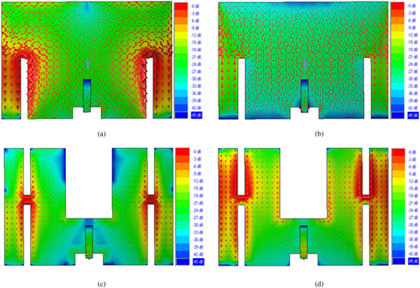
The radiating patch is printed on substrate RT Duroid 5880 with the thickness 1.59 mm. The patch is separated by air gap spacing of 10 mm from the ground plane. The fabricated antenna is shown in Fig. 4. The patch is electromagnetically coupled by a conducting strip connected with the probe. This conducting strip of dimensions l s × w s is printed above the radiating patch and both are separated by a dielectric substrate of thickness t = 1.59 mm. Such feeding method is more convenient than the conventional L-strip fed patch. The perturbed structure introduces some additional current to flow in the patch which causes the higher modes to shift closer and hence a wideband characteristics of the antenna is observed. Therefore, the current distributions on the two antennas are shown in Fig. 5 at two resonant frequencies 2.1 and 2.5 GHz, respectively. From this figure, it is clear that the current length can be optimized by introducing some notches along the radiating edges. The dimensions of the notches are taken in such a way so that the wideband nature of the antenna can be realized. The current distribution curves indicate that the lower resonance is produced by two parallel notches in the patch while the higher one is created due to the combined effect of the initial patch and the notches.

Fig. 4. Prototype of the fabricated antenna (a) antenna-I (b) antenna-II (c) bottom view (d) top view.

Fig. 5. Current distribution using IE3D at two resonant frequencies 2.1 and 2.5 GHz for antenna-I (a) and (b), and for antenna-II (c) and (d).
Results and discussion
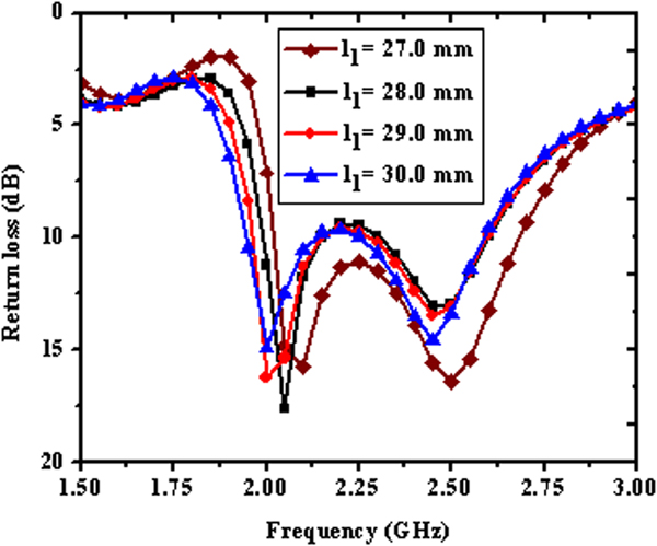
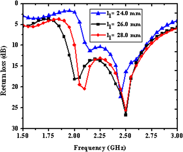
It is noted that all the antenna parameters are calculated using HFSS simulator for antenna-I and antenna-II. For antenna-I, the variation of return loss with frequency for different values of notch width (w 1) is shown in Fig. 6. From the figure, it is observed that the bandwidth increases as w 1 increases. It is found that as notch length l 1 increases (for a given value of w 1 = 3.0 mm) the operational frequency band shifts towards the lower side with a slight increase in bandwidth as shown in Fig. 7. The operational frequency band for antenna-I, calculated using HFSS, extends from 1.91–2.66 GHz and bandwidth obtained is 32.82%. The fabricated antenna is measured using Vector Network Analyzer with model type-Agilent N5230A. The measured bandwidth for antenna-I is found to vary from 1.92–2.67 GHz (32.68%). Theoretical and simulated return loss results are compared with the measured results which are in good agreement (Fig. 8). Return loss is also plotted for antenna-II in Fig. 9 and it is observed that the bandwidth significantly increases with the increasing value of l 1. Similar results are also found in case of increasing value of l 2 (Fig. 10).

Fig. 6. Variation of return loss with frequency for different value of w 1 (l 1 = 26.0 mm is fixed) for antenna-I.

Fig. 7. Variation of return loss with frequency for different values of l 1 (w 1 = 3.0 mm is fixed) for antenna-I.

Fig. 8. Comparative graph of return loss with frequency for antenna-I, (w 1 = 3.0 mm and l 1 = 26.0 mm).

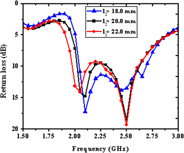
Fig. 9. Variation of return loss with frequency for different values of l 1 (l 2 = 20.0 mm, w 1 = w 2 = 3.0 mm) for antenna-II.

Fig. 10. Variation of return loss with frequency for different values of l 2 (l 1 = 26.0 mm, w 1 = w 2 = 3.0 mm) for antenna-II.
From Fig. 11, it is found that the bandwidth marginally increases as the length of center notch l 3 increases, however; the patch size is reduced upto 30% as compared with the conventional rectangular patch. Thus, for a particular dimension, one can achieve a miniaturized antenna with appreciable bandwidth. The results for antenna-II obtained from HFSS, IE3D, and proposed theory are in agreement with the measured results (Fig. 12). The operational frequency band for this antenna, calculated using HFSS, is varying from 1.93 to 2.83 GHz and the bandwidth obtained is 37.82%. The measured frequency band for antenna-II is found to vary from 1.94 to 2.74 GHz (34.19%). Some deviation in the simulated and measured results is due to fabrication imperfection and the misalignment of SMA connector. The gain measurement is performed inside an in-house anechoic chamber of physical dimensions 7.0 × 5.0 × 3.0 m3 and shown in Fig. 13. A Dual Ridge Horn Antenna (DRH20) of size 56 × 41 × 18 cm3 is used for the gain measurement. The gains of antenna-I and antenna-II are measured from 1.5 to 3.0 GHz with an equal frequency interval of 0.1 GHz. Measured gains for both the antennas are shown in Figs 14 and 15, respectively. The discrepancy between simulated and measured gain of antennas may be due to the fact that no near-field to far-field correction is applied for the direct measurement. Another reason is due to the use of DRH horn antenna which is somewhat not suitable for such type of correction. It is observed that the gain is always above 6.5 dBi for the entire band of operation. The maximum measured gain for antenna-I and antenna-II are 8.43 and 8.39 dBi, respectively. The measured average gain for antenna-I and antenna-II are calculated and found to be 7.23 and 7.63 dBi, respectively. The comparisons of the proposed antennas performance are illustrated in Table 2. The proposed antennas exhibit sufficient bandwidth and high gain as compared with the earlier reported antennas.
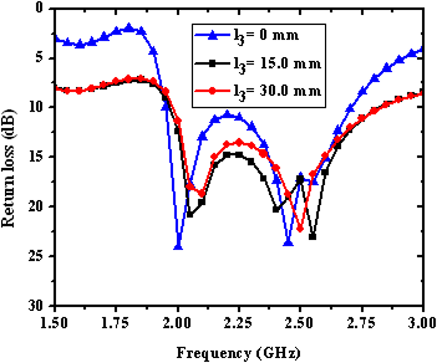
Fig. 11. Variation of return loss with frequency for different values of l 3 (w 3 = 20.0 mm is fixed) for antenna-II.

Fig. 12. Comparative plot of return loss with frequency for antenna-II (l 3 = 30 mm, w 3 = 20.0 mm, l 1 = 26 mm, w 1 = w 2 = 3 mm).

Fig. 13. Gain measurement setup.

Fig. 14. Measured gain for antenna-I.

Fig. 15. Measured gain for antenna-II.
Table 2. Comparison of the proposed antennas with earlier reported antennas.

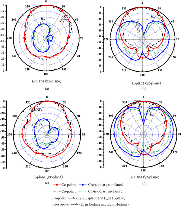
The radiation patterns measured for antenna-I and II are plotted in Figs 16 and 17 at φ = 00 (E plane) and φ = 900 (H plane) for two resonant frequencies (2.1 and 2.5 GHz), respectively. The cross-polarization level is quite low as compared with co-polarization level for both the antennas at φ = 0° and φ = 90°. The radiation patterns of the proposed antennas are symmetrical, broadside in nature and linearly polarized. E and H plane half power beamwidths (HPBW) is measured for both the antennas at 2.1 and 2.5 GHz, respectively. For antenna-I, the E and H plane HPBW are 57.8° and 61° at 2.1 GHz and 45.48° and 58.68° at 2.5 GHz, respectively. For antenna-II, the E and H plane beamwidths are 58.14° and 63.05° at 2.1 GHz and 45.41° and 54.24° at 2.5 GHz, respectively. Also, it is noted that the simulated and measured values of beamwidths are in good agreement.

Fig. 16. Simulated (HFSS) and measured radiation pattern of antenna–I at f = 2.1 GHz (a and b) and at f = 2.5 GHz (c and d).

Fig. 17. Simulated (HFSS) and measured radiation pattern of antenna–II at f = 2.1 GHz (a and b) and at f = 2.5 GHz (c and d).
Conclusion
A modified L-strip feeding technique is used to study the slotted patch antennas. The circuit theory is successfully implemented to calculate the antenna parameters. From this study it is inferred that the antenna bandwidth is function of dimensions of the notches incorporated in the patch. Antenna size is also reduced along with the enhancement of bandwidth. Radiation pattern is stable and gain is acceptable across the entire operational band. The dimension of conducting strip may also be the key parameters for further improvement in the antenna performance, which is not studied in the present paper. The proposed antennas can be used for WiFi/Bluetooth, UMTS, radio frequency identification device (RFID) and other communication systems.
Author ORCIDs
Prabhakar Singh, Binod Kumar Kanaujia 0000-0001-8272-3293, 0000-0003-1272-1561.
 Rakesh Nath Tiwari received his B.Sc. and M.Sc. (Electronics) degree from University of Allahabad and Deen Dayal Upadhyaya Gorakhpur University, Gorakhpur, India in 2002 and 2004, respectively. He received M.Tech. degree in Optical & Wireless Communication Technology from Jaypee University of Information Technology, Waknaghat, Solan, India in 2008. He has published more than 21 papers in peer-reviewed International/National journals and conferences. Currently, he is a Ph.D. scholar in Electronics and Communication Engineering from Uttarakhand Technical University, Dehradun, India. His research interests include design and modeling of slot patch antennas, UWB antennas, microwave/millimeter wave integrated circuits & devices.
 Prabhakar Singh was born in village Semara, Chandauli (U.P), India in 1984. He received his B.Sc. and M.Sc. degree from V. B. S. Purvanchal University in 2004 and 2006, respectively. He received his Ph.D. degree from J. K. Institute of Applied Physics, Department of Electronics and Communication, University of Allahabad, India in 2010. He taught B. Tech. and M. Tech. students at Delhi Technological University, Delhi, India for 1 year from 2009 to 2010. He worked as an assistant professor at Bahra University, Shimla Hills, Himanchal Pradesh, India from 2010 to 2011. Presently, he is working at Galgotias University, Greater Noida, India. He has published more than 50 research papers in peer reviewed International/National journals and conference proceedings with more than 400 citations. He is reviewer of many International and National journals. He is presently working on broadband microstrip antennas, size miniaturization techniques in patch antennas, UWB and photonic band gap antennas.
 Binod Kumar Kanaujia is working as Professor in School of Computational and Integrative Sciences, Jawaharlal Nehru University, New Delhi since August, 2016. Before joining Jawaharlal Nehru University, he had been in the Department of Electronics & Communication Engineering in Ambedkar Institute of Advanced Communication Technologies & Research (formerly, Ambedkar Institute of Technology), Delhi as a Professor since February 2011& Associate Professor (2008–2011). Earlier, Dr. Kanaujia held the positions of Lecturer (1996–2005), Reader (2005–2008) and Head of Department in Department of Electronics & Communication Engineering, M.J.P. Rohilkhand University, Bareilly, India. Prior to his career in academics, Dr. Kanaujia had worked as Executive Engineer in the R&D division of M/s UPTRON India Ltd.
Dr. Kanaujia had completed his B.Tech. in Electronics Engineering from KNIT Sultanpur, India in 1994. He did his M.Tech. and Ph.D. in 1998 and 2004; respectively from Department of Electronics Engineering, Indian Institute of Technology Banaras Hindu University, Varanasi, India. He has been awarded Junior Research Fellowship by UGC Delhi in the year 2001–2002 for his outstanding work in the electronics field. He has a keen research interest in design and modeling of microstrip antenna, dielectric resonator antenna, left-handed metamaterial microstrip antenna, shorted microstrip antenna, ultra-wideband antennas, reconfigurable and circular polarized antennas for wireless communication.
He has been credited to publish more than 220 research papers with more than 1000 citations with h-index of 17 in several peer-reviewed journals and conferences. He had supervised 50 M.Tech. and 15 Ph.D. research scholars in the field of microwave engineering. He is a reviewer for several journals of international repute i.e. IET Microwaves, Antennas & Propagation, IEEE Antennas and Wireless Propagation Letters, Wireless Personal Communications, Journal of Electromagnetic Wave and Application, Indian Journal of Radio and Space Physics, IETE Technical Review, International Journal of Electronics, International Journal of Engineering Science, IEEE Transactions on Antennas and Propagation, AEU-International Journal of Electronics and Communication, International Journal of Microwave and Wireless Technologies, etc. Dr. Kanaujia had successfully executed 05 research projects sponsored by several agencies of Government of India i.e. DRDO, DST, AICTE, and ISRO. He is also a member of several academic and professional bodies i.e. IEEE, Institution of Engineers (India), Indian Society for Technical Education and The Institute of Electronics and Telecommunication Engineers of India.