


Introduction
Dielectric resonator (DR) antenna (DRA) offers wide bandwidth, high gain, high radiation efficiency with minimal surface wave and conductor losses [Reference Mongia and Bhartia1]. These features of DRA made it popular among the researchers. Earlier, the study was carried out on the linearly polarized (LP) DRA (LPDRA). It was observed that the misalignment of LP antennas causes polarization mismatch losses. Also, the signal degradation occurs in the case of the multipath reception if LPDRA is being used in a communication system. Replacing the LP antenna with a circularly polarized (CP) antenna prevents these limitations, so the development of CPDRA was promoted [Reference Toh, Cahill and Fusco2]. To achieve the circular polarization in DRA, numerous techniques have been reported in the literature [Reference Sulaiman and Khamas3–Reference Varshney14]. Some of these can be categorized as single feeding, dual feeding, modified shape of the DR, and modified shape of the slot. The limitation of single feeding technique is that it provides a narrow axial ratio (AR) bandwidth [Reference Sulaiman and Khamas3, Reference Tam and Murch4]. To increase the AR bandwidth, dual feeding structure was reported [Reference Pan, Leung and Lim5]. However, dual feeding structure becomes complex due to the requirement of the external power dividers. Later on, the shape of the DR was modified to increase the CP bandwidth, e.g., trapezoidal [Reference Pan and Leung6], stair shape [Reference Fakhte7], rotating stair [Reference Wang and Wong8], DR with diagonally inclined slits [Reference Khalily, Kamarudin and Jamaluddin9], and DR with parasitic strips [Reference Pan and Leung10]. These antennas provide wide CP bandwidth but the complexity of DR shape leads to the manufacturing difficulty. To achieve wide AR bandwidth, different shapes of the slot have been proposed like cross slot [Reference Huang, Wu and Wong11], modified cross slot [Reference Pan and Zou12], Archimedean spiral slot [Reference Zou, Pan and Nie13], and stair-shaped slot [Reference Varshney14]. The use of the specific shaped slot in the antenna structure with single feeding provides wide CP bandwidth. Recently, a CPDRA was reported with stair-shaped slot providing wide AR and impedance bandwidths of 41.01 and 49.67%, respectively [Reference Varshney14]. Despite significant progress, obtaining the wide CP bandwidth with simple DR structures and single feeding is still a challenging task.
In this context, this paper presents a new technique for the enhancement of AR bandwidth of CPDRA. The proposed antenna structure provides the multiple 3-dB AR passbands. The neighboring 3-dB AR passbands of the antenna are merged to enhance the AR bandwidth by introducing the notches and conductive coating in the DR. Previously, the diagonal vertices of the DR were removed to achieve the dual-band circular polarization [Reference Ngan, Fang and Leung15]. Also, a CP antenna array was proposed with the chamfered DR structure [Reference Haneishi and Takazawa16]. Achieving the circular polarization in chamfered DR with aperture feeding is easy when the length and width aspect ratio of the rectangular DR is unity. When this aspect ratio of the rectangular DR is non-unity, the size of the notches must be selected prudently. In this paper, a rectangular DR is used with non-unity length/width aspect ratio. The size of the notches is selected so that the impedance bandwidth of antenna remains unaffected. After that conductive coating is applied on the notched wall of the DR for merging of the adjacent AR passbands. Earlier, parasitic strips were used in a complex DR structure to achieve the AR and impedance bandwidths of 25% and 24.5%, respectively [Reference Pan and Leung10]. The stair-shaped slot is used for excitation in the proposed antenna structure [Reference Varshney14]. The proposed antenna provides the measured 3-dB AR bandwidth of 55.22% and 10-dB impedance bandwidth of 66.45%. The 3-dB AR passband completely overlaps with the 10-dB impedance passband which makes the antenna useful for C-band applications. Furthermore, the antenna structure is simple and needs single feeding. The use of conductive coating at the notched corner of the DR is a simple and novel technique for the enhancement of AR bandwidth of a CPDRA.
Antenna configuration
The geometry of the proposed CPDRA is shown in Fig. 1. Antenna structure contains a substrate of FR_4 epoxy with permittivity ε s = 4.4 that has the dimensions l g × w g and thickness 0.8 mm. RF excitation is applied through an SMA connector which is connected to a 50 Ω microstrip line. The microstrip line has the dimensions l m × w m. The stub of length s is used for impedance matching. The field is coupled from the microstrip line to DR through a stair-shaped slot in ground plane at the top of the substrate. The orthogonal modes necessary for circular polarization are generated using the stair-shaped slot [Reference Varshney14]. The working mechanism of the feeding through stair-shaped slot is already reported and explained in [Reference Varshney14]. The dimensions of DR are selected using dielectric waveguide model to operate at 4.75 GHz [Reference Mongia and Bhartia1]. The selected aspect ratio of the DR allows to operate with fundamental, second, and third order modes [Reference Zhang, Li and Lv17]. This structure of rectangular CPDRA provides a wide overlapped AR and impedance bandwidth. To enhance the CP bandwidth of the antenna, two opposite corners of rectangular DR are notched. The side wall of the notched top corner is coated with a conductive material as shown in Fig. 1(a). The conductive coating works as a parasitic strip. The antenna structure was analyzed using high-frequency structure simulator based on finite element method and fabricated. Figures 1(b) and 1(c) show the fabricated CPDRA. The ceramic material with the permittivity ε r = 12.8 is used to fabricate the DR height h. All the optimized dimensions of antenna structure are mentioned in the caption of Fig. 1.
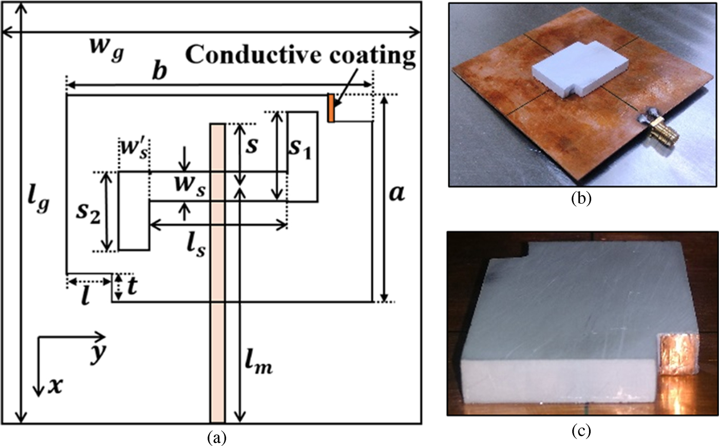
Fig. 1. (a) Geometry of the proposed CPDRA, (b) fabricated antenna prototype and (c) side view of the fabricated DR showing conductive coating. a = 24, b = 33, h = 5, s 1 = 10.1, s 2 = 7, l s = 13, w s = 1.5, w′s = 2.5, s = 7, l m = 40, w m = 1.6, l = 6, t = 4.6, l g = 80 and w g = 80 (all dimensions of the antenna structure are in mm).
Antenna operation
For the understating of antenna operation, three antenna structures are shown in Fig. 2, designed and analyzed. The first antenna structure (antenna-1) contains a rectangular DR. In second antenna structure (antenna-2), the diagonally opposite corners of DR are notched. In the third antenna structure (antenna-3), the side wall of the notched top corner of the DR is coated with a conductive material. Figure 3 shows the AR and S 11 parameter response and Table 1 shows the performance of all these antenna structures. There are two nearby 3-dB passbands in the AR plot of antenna-1, lower 4.28 − 6.64 GHz, and upper 7.70 − 8.05 GHz. This antenna provides the simulated 3-dB AR bandwidths of 43.22% in the lower and 4.44% in the upper band. AR plot of antenna-1 shows that the level of AR is around 18 dB between lower and upper 3-dB passbands. This antenna provides the impedance bandwidth of 66.34% (4.16 − 8.29 GHz). AR plot of antenna-2 shows that introduction of the notches in DR widen the 3-dB AR bandwidth of lower band. Also, upper 3-dB AR passband of antenna-2 is shifted towards the lower 3-dB AR passband as shown in Fig. 3(a) and mentioned in Table 1. The level of the AR goes below 5 dB between lower and upper 3-dB passbands. The impedance bandwidth of antenna-2 is 67.09% (4.17 − 8.38 GHz). Notches in the DR create the air gap, due to which the quality factor of the DR decreases that leads to the slight increment in the impedance bandwidth of antenna-2 [Reference Chang and Kiang18].
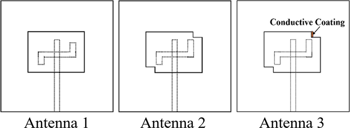
Fig. 2. Top view of the three CPDRAs.

Fig. 3. The frequency response of (a) AR, (b) S 11 parameter, and (c) gain plot of the three antenna structures.
Table 1. Comparison of performance of all antennas.

The length and width of the notches are kept smaller (l, t ≈ 0.1λ) so there is no significant change in the overall quality factor of the antenna. Now, the conductive coating is applied at the notched corner of the DR. The conductive coating on the side wall of the notched DR slightly increases the quality factor [Reference Pan and Leung10]. Consequently, impedance bandwidth of antenna-3 is slightly reduced. The AR plot of antenna-3 shows that both 3-dB AR passbands are merged which increases the overall 3-dB AR bandwidth. Furthermore, the introduction of the conductive coating does not increase the structural complexity to the antenna because it can be applied only by pasting the easily available copper tape. Table 1 shows that there is 8–11% enhancement of the AR bandwidth only by applying the conductive coating. Merging of the bands can be understood as E x component of the field is generated by the main slot and side slots generate the E y component [Reference Varshney14]. For merging of the bands, it is necessary to increase the amplitude of E y component equivalent to E x component of the field. Therefore, the location of the conductive coating is kept closer to the longer side arm of the slot. This reinforces the E y components, due to which the level of AR goes below 3 dB between lower and upper bands. Consequently, both 3-dB AR passbands are merged and a wide 3-dB AR bandwidth is achieved. Figure 3(c) shows the gain performance of all the antenna structures. There is a small difference in the peak gain of all the antenna structures. Antenna-3 provides the CP radiations at frequencies 4.75, 6.02, and 7.21 GHz and operates with modes TE 111, TE 121, and TE 131, respectively. The E-field distribution inside the proposed DR are similar to those were reported by Zheng et al. [Reference Zhang, Li and Lv17]. Figure 4 shows the E-field distribution at the top surface of DR corresponding to these modes. The E-field distribution is rotated at an angle due to CP operation of the antenna. The CP operation of the antenna can be confirmed from Fig. 5. Here, the E-field vectors are represented at the different time instants. Figure 5 shows that E-field vectors rotate and complete a circular path. The field vectors are rotating in the anticlockwise direction, which confirms the right-hand CP (RHCP) operation.

Fig. 4. E-field distribution at the DR top surface at frequency (a) 4.75 GHz, (b) 6.02 GHz and (c) 7.21 GHz (amplitude of the E-field is shown in color bar).
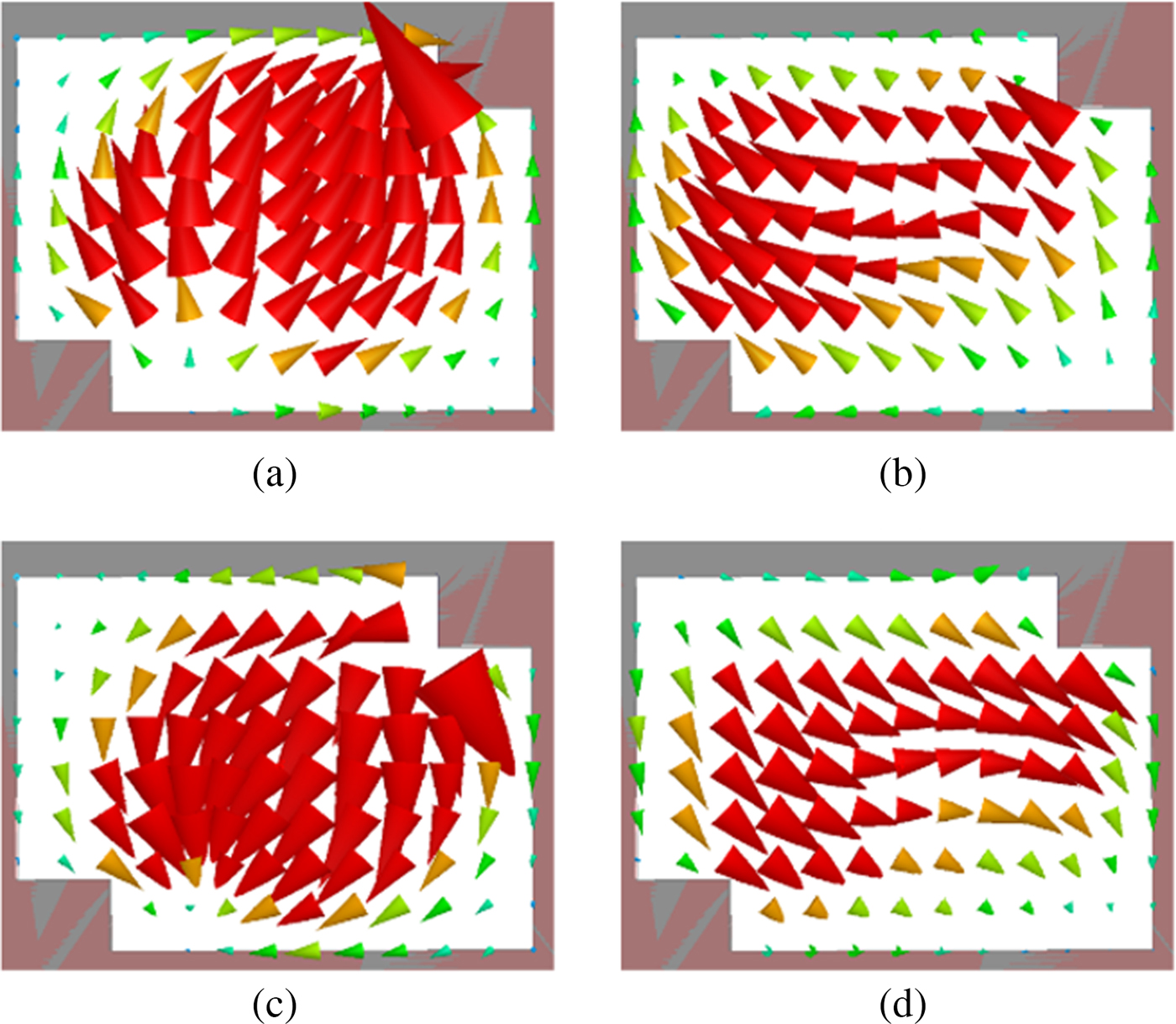
Fig. 5. E-field vectors at the top surface of the DR at frequency 4.75 GHz at time (a) t = 0, (b) T/4, (c) T/2, and (d) 3T/4.
Parametric study
A parametric study has been carried out to obtain the optimum dimensions of the antenna for which CP modes are appropriately excited inside the antenna structure.
Variation of the notch length, l
Figure 6(a) Shows that variation of notch length, l mainly affects the AR at the frequency of the third-order CP mode. The AR remains below 3 dB at the frequencies of the lower order modes. The impedance bandwidth of the antenna is same with the variation of l as shown in Fig. 6(b). The optimum results are obtained at l = 6 mm.
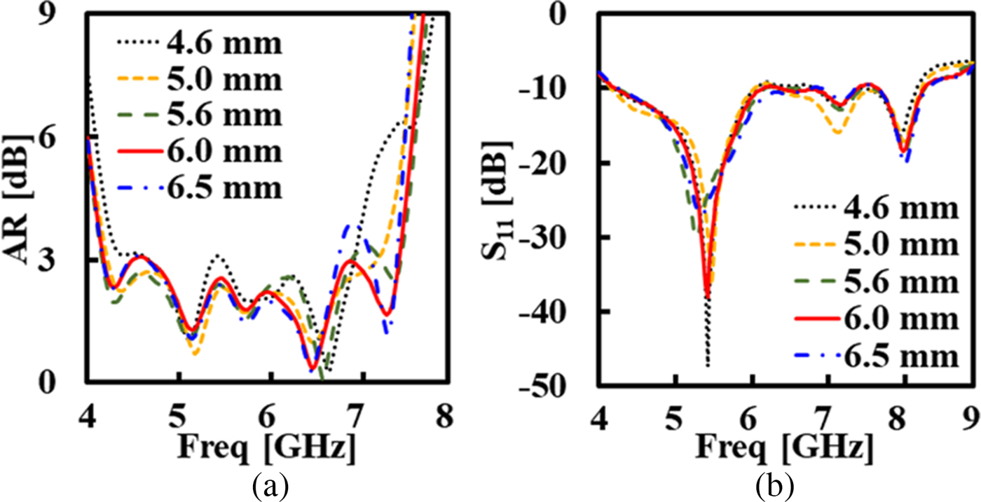
Fig. 6. The frequency response of (a) AR and (b) S 11 parameter for variable l.
Variation of the notch and strip width, t
Figure 7(a) shows that the variation of t affects the AR response at the frequencies of the first and second-order CP modes. With the increment in t, the level of AR increases at the frequency of the first order mode, while it decreases at the frequency of the second-order mode. The optimum value of t is 4.6 mm for which a wider 3-dB AR bandwidth is obtained. Figure 7(b) shows that the impedance bandwidth of the antenna is unchanged with the variation of t.
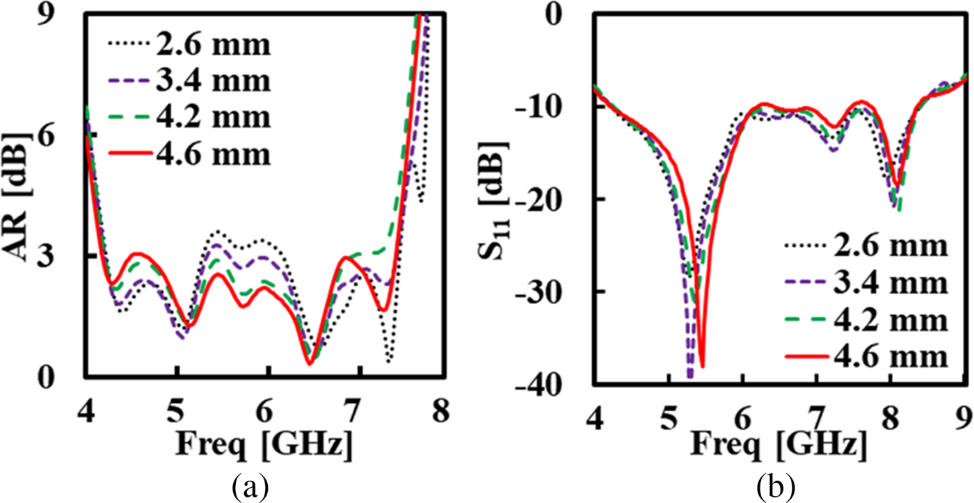
Fig. 7. The frequency response of (a) AR and (b) S 11 parameter for variable t.
Variation of the slot length, s 1
Figure 8 shows the AR and S 11 parameter response with the variation of s 1. Variation of s 1 allows the tuning of AR response below 3 dB as shown in Fig. 9(a). For the values of s 1 from 10.1 to 11.0 mm, fields are appropriately coupled to DR from the slot which results in wider 3-dB AR bandwidth. For s 1 < 10.1 mm, 3-dB AR bandwidth decreases due to the reduction in the separation between resonant frequencies of CP modes. For s 1 > 11 mm, AR response goes above 3 dB. Figure 8(b) shows that impedance bandwidth of the antenna is not affected by variation of s 1.
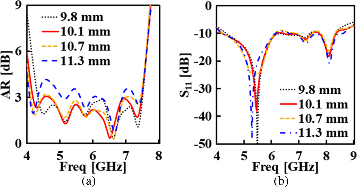
Fig. 8. (a) AR and (b) S 11 parameter response for variable s 1.
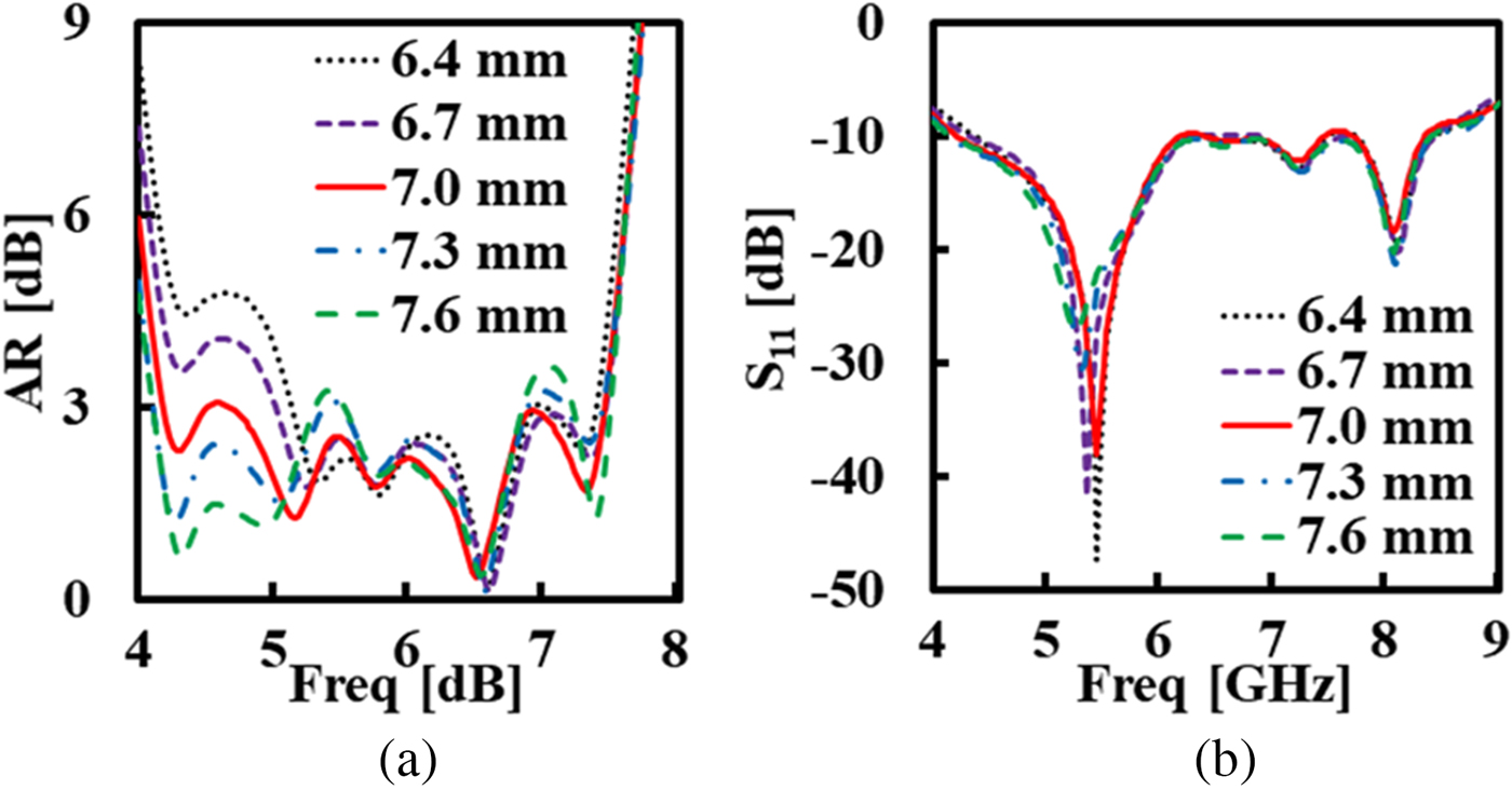
Fig. 9. (a) AR and (b) S 11 parameter response for variable s 2.
Variation of the slot length, s 2
Figure 9(a) shows that AR response of the antenna can be tuned at a frequency of the first CP mode. Increment of s 2 lowers the level of AR only at the frequency of fundamental mode. Whereas, the AR response remains stable at the frequencies of other higher order modes. Figure 9(b) shows that the variation of s 2 does not affect the impedance bandwidth of the antenna.
Variation of the DR height, h
Figure 10 shows the effect of variation of h on antenna response. Increasing h enhances the gain of the antenna as shown in Fig. 10(c). The S 11 parameter response of the antenna shifts in the backward direction as usual as shown in Fig. 10(b). The variation of h drastically affects the AR response. It becomes difficult to maintain the AR response below 3-dB for a wide frequency band as shown in Fig. 10(a).
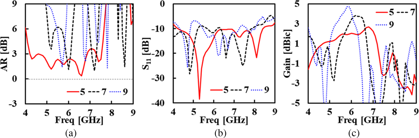
Fig. 10. (a) AR, (b) S 11 and (c) gain response for variable h.
Results and discussion
The prototype of antenna-3 was fabricated (Figs 1(b) and 1(c)) and results were measured. Figure 11 shows the simulated and measured AR and S 11 parameter response of the proposed CPDRA. The AR of the antenna is measured using satimo star lab system. The antenna provides 56.57% (4.17 − 7.46 GHz) simulated and 55.22% (4.26 − 7.51 GHz) measured 3-dB AR bandwidth in the boresight direction(θ = 0°). The simulated and measured 10-dB impedance bandwidth of the antenna is 66.24% (4.19 − 8.34 GHz) and 66.45% (4.17 − 8.32 GHz), respectively. Figure 12 shows the radiation pattern of the antenna in xz and yz-planes at different frequencies where minima were obtained in AR passband. The RHCP patterns are 15 dB or more dominating over the left-hand CP patterns in boresight (θ = 0°) direction that confirms the RHCP operation of the antenna. The radiation pattern of the antenna is broadside and almost stable in the observed frequency band. Figure 13(a) shows the gain plot of the antenna. The gain plot shows the peaks at the resonant frequencies of the modes with which antenna operates and decreases at other frequencies. The simulated and measured peak value of gain is 2.67 and 2.06 dBic, respectively; it is achieved near the resonant frequency of third-order mode in the passband of the antenna, as expected. Figure 13(b) shows plot for simulated radiation efficiency of antenna, it is more than 80% in the passband. Figure 13(c) shows the AR plot, which illustrates 3-dB AR beamwidth of the antenna at frequency 4.75 GHz. The antenna provides 3-dB AR beamwidth of 158° and 123° in xz and yz -planes, respectively, in boresight direction. Table 2 shows a comparison of the proposed CPDRA with other antennas. It is observed that proposed CPDRA provides the wide impedance and AR bandwidth. In addition, the whole 3-dB AR and 10-dB impedance passbands overlap and overlapping bandwidth is comparatively wide. This was the limitation of most of the reported antenna structures that both passbands do not overlap [Reference Khalily, Kamarudin and Jamaluddin9, Reference Pan and Leung10].
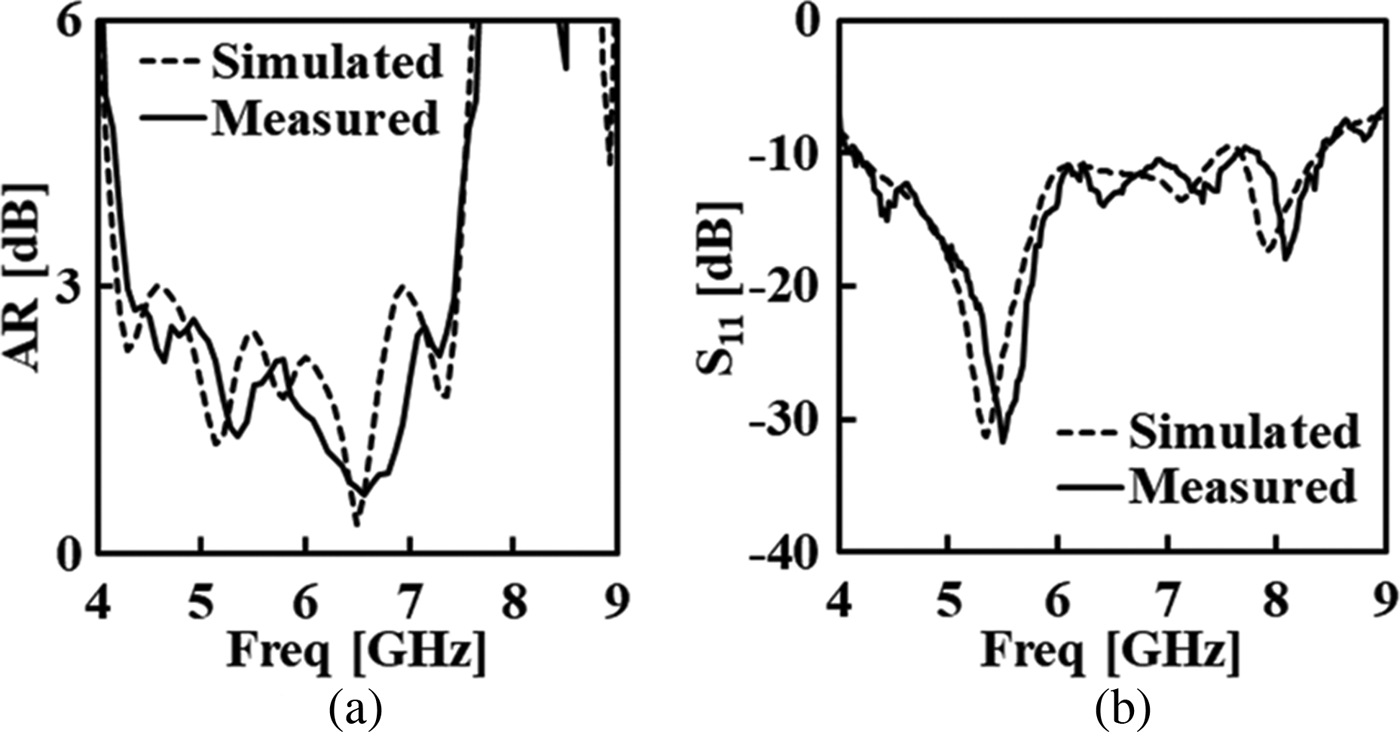
Fig. 11. (a) AR and (b) S 11 parameter response of the proposed CPDRA.

Fig. 12. Radiation pattern of the antenna at frequency (a) 4.28, (b) 5.14, (c) 5.78, and (d) 6.5 GHz (Images at top side are in xz plane and at bottom side are in yz plane).
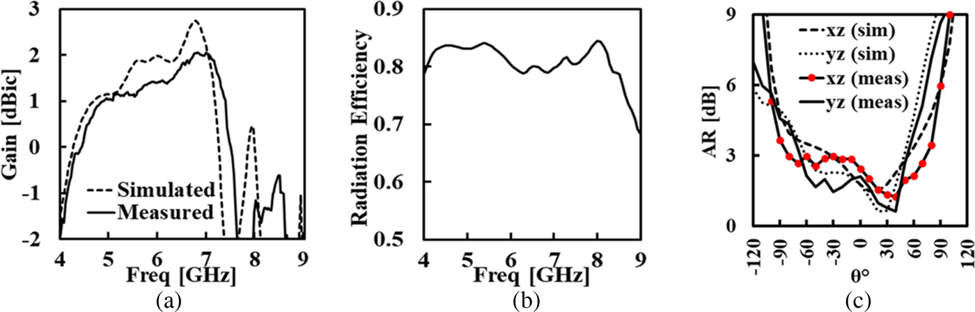
Fig. 13. (a) Gain and (b) radiation efficiency as a function of frequency, and (c) AR as a function of angle θ°.
Table 2. Comparison with other CPDRAs.

Conclusion
A technique has been implemented to enhance the AR bandwidth of CPDRA with a single feeding. The upper 3-dB AR passband is merged to the lower 3-dB AR passband. Consequently, a wide CP bandwidth has been achieved. The measured 3-dB AR and 10-dB impedance bandwidths of 55.22 and 66.45%, respectively, have been achieved. The antenna offers 3-dB AR beamwidth of 158° and 123° in xz and yz-planes, respectively.
Acknowledgement
Authors are thankful to Mr. V. Pasricha, G. R. Kumar, and A. P. Singh, BEL India for providing the support in measurement.
 Gaurav Varshney completed B. Tech in Electronics and Communication Engineering from UPTU, M. Tech in RF and Microwave Engineering from AIACTR Delhi. Currently, he is a senior research fellow in Department of Electronics and Communication Engineering at NIT Delhi, India. He has authored high-quality research papers published in peer-reviewed journals including IEEE Transactions on Antennas and Propagation, IET Microwave, Antennas and Propagation, and others. His research interests include the microwave and millimeter wave antennas and dielectric resonator antennas. https://goo.gl/P8JfCf.
 Dr. V. S. Pandey completed B. Sc. in 1998, M. Sc. in 2000 and Ph.D. in 2006 from IIT BHU, Varanasi. He became the Post-Doctoral Fellow at Department of Space, Government of India from 2007 to 2009. He became the Post-Doctoral Associate from August 2009 to July 2012 and the Research Professor at World Class University (WCU) Project-under the collaboration of KAS/JAXA and NASA, at School of Space Research, Kyung Hee University, South Korea from August 2012 to July 2013. Currently, he is working with the Department of Applied Sciences, National Institute of Technology, Delhi, India. He had significantly contributed to the research areas of Antenna Designing, RF and Microwave devices, Space Physics, Magneto-hydrodynamics fields and waves. Currently, he is the referee of various world-class journals.
 R. S. Yaduvanshi has 24 years of teaching and research experience. He has successfully implemented fighter aircraft arresting barrier projects at select flying stations of Indian Air Force. He has worked on Indigenization projects of 3D radars at BEL and visited France for Radar Modernization as Senior Scientific Officer in Ministry of Defence. Currently, he is working on MHD projects. He is working as a professor at Ambedakar Institute of Advanced Communication Technologies and Research (AIACTR), Government of Delhi, India. He has authored several research papers in peer-reviewed journal and books with good impact.


