I. INTRODUCTION
The integration of analog circuits to radio frequency-integrated circuits (RFICs) incorporating all circuit stages of a radio frontend has become more feasible with current SiGe technologies and the utilization of signal processing in RF, e.g. altering amplitudes and phases for multiple input multiple output (MIMO) or beamsteering operations [Reference Paulraj, Nabar and Gore1] is nowadays common practice. Accordingly, the demand of linear matched driver circuits for a variety of operations has increased. However, low-power operation and linearity requirements are counteracting figures, which prevented class-B circuits from a widespread use in RF signal paths. For example the driver of an allpass network employed in vector modulators [Reference Mayer, Wickert, Eickhoff and Ellinger2] has to maintain a constant low-ohmic output impedance and a high dynamic range, which typically makes the class-A common collector (CC) stage the circuit of choice in this application. But this topology suffers from a very low achievable linear output power and low efficiency both of which can be enhanced by the totem-pole (TP) topology. Although the concept of TP stages [Reference Yeh3] is used by some designers [Reference Koh and Rebeiz4], a thorough analysis of TP stages and their limits in RF applications is still missing in the literature. Although in [Reference Tiiliharju, Pellikka and Halonen5] the general suitability of TP stages for high-power broadband drivers is also confirmed, our investigation, however, does not conclude the 50% bandwidth penalty of the TP stage stated in [Reference Tiiliharju, Pellikka and Halonen5]. Because of the high integration level in currently developed RF frontends, differential signaling is used nearly everywhere to reduce undesired coupling and disturbing effects, which is why this investigation assumes differential signal sources despite the higher system and power demand [Reference Issakov, Knapp, Bakalski, Wojnowski, Thiede and Simbürger6].
At first this paper reviews the TP driver's properties in comparison with the CC driver. Section III explains a design guideline for different optimization requirements, while Section IV extends the TP driver toward wideband applications. Section V provides results from a successful implementation in an RF combiner chip. Section VI concludes the analysis.
II. COMPARISON OF TP AND CC STAGE
A) Topology explanation
The single-ended representation of a CC driver depicted in Fig. 1(a) operates in class-A, making the drive of current amplitudes greater than I 0 into R load impossible. Thus, the maximum linear output power is restricted by the chosen bias current I 0 required for broadband matching behavior which is given by I 0 = V T/R load. The maximum distortion free output power is hence limited to P out = 0.5I 02R L. For R load = 50 Ω the required current is I 0 = 520 µA, which limits the output power to P out = −21.7 dBm. However, if the current source itself is modulated by the inverse of the input signal like in a TP stage (Fig. 1(b)), both transistors contribute additively to the output current and hence, the achievable output power is increased, while keeping the same matching properties of the CC stage. Because of the non-linear properties of T 2 the bias point is moved up for higher drives yielding in reduced output resistance of the CC stage, which compensates for the resistance increase due to the off-times of T 1 at higher input levels. Thus, the desired output impedance can be maintained for large-signal excitations up to very high output amplitudes.

Fig. 1. Analyzed drivers and small-signal equivalents: (a) CC and (b) TP.
B) Small-signal properties
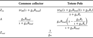
The analysis, using the simplest representation of the circuits, assuming a transistor model consisting of base emitter resistance r BE and transfer current source g m neglecting frequency-dependent parameters as well as the bias resistor R bias. This model yields the differential small-signal characteristics listed in Table 1.
Table 1. Differential small-signal comparison (g mr BE≪1).

With the assumption Z source≪r BE in the case of ideal output matching (Z out = Z load*) the transistor's transconductance g m = I CA/U T has to equal g m = 1/R load. Since real transistors typically use highly doped polysilicon emitters at tens to hundreds Ω/µm2 yielding in emitter resistances r ex of several to tens Ω for SiGe [Reference Ashburn7], it is necessary to increase g m so that 1/g m + r ex = R load, which completes the design of the CC driver. In a TP stage it is desirable to maximize the voltage gain by lowering R e or increasing g m. While a further increase of g m worsens the output matching, the influence of R e shall be analyzed in the following:
(1) R e influences the input impedance Z in. For practical ranges of R e, Z in in a TP stage is reduced by max. 33% compared with the CC stage, which in typical applications with source impedances of several hundred ohms is still sufficiently high.
(2) R e has strong impact on the voltage gain A as visualized in Fig. 2(a). Both transistors of the TP stage are affected by R e: the emitter stage in the well-known series feedback manner, and the collector stage due to the virtual load increase dependent on R e.

Fig. 2. TP small-signal behavior: (a) voltage gain and (b) virtual load resistances.
The small-signal behavior of the TP stage can be explained considering the effective load impedances seen by the two transistors. Those virtual loads defined by Z load, virtual = v out/i T determine the output current contribution of each transistor and are derived with the assumption g mr BE≪1 yielding the DC terms listed in Table 2 and plotted in Fig. 2(b).
Table 2. Effective load impedances seen by T 1 and T 2.
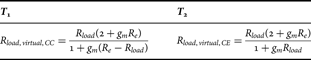
If clipping of the two transistors should occur at the same input level, it is desirable that both transistors contribute equally to the output current (Fig. 2(b)), which requires R e = 2R load. Then from the small-signal equivalent circuit (Fig. 1) an identical behavior of the two transistors is observable.
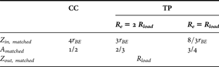
For reasons of optimized large-signal operation (compare Section II(C)) a lower R e is favorable and included in Table 3. If R e is chosen very low, all the gain is provided by the common emitter stage T 2 making the contribution of T 1 negligible, which equals an effective load resistance of T 1 close to infinity. This case is shown in Fig. 2(b) for the perfectly matched condition g m = 1/R load. At higher g m > 1/R load the lower limit for decreasing R e and thus, achieving higher output voltage, is formed by R e = R load − 1/g m, at which the small-signal current contribution of T 1 vanishes and force T 1 to operate counteracting to T 2 thereby yielding negative load resistances. Thus, the boundaries for the optimizing task of R e are set.
Table 3. Small-signal parameters in matched case (Z out = Z load*).
Incorporating the most relevant resistors (r bx) and capacitances (c je, c jc) into the small-signal transistor model yields nearly equivalent bandwidths for both drivers (cf. Fig. 3). The obtained 1 dB bandwidths for a 500 Ω source are 4.9 and 5.0 GHz for the CC stage and the TP stage, respectively. If the source impedance is reduced to 100 Ω the bandwidths increase to 15.1 and 17.4 GHz. The most relevant bandwidth limit in both configurations is the pole introduced by c je and R S′ = R source + r bx. Hence, the highest bandwidths can be achieved using a low ohmic signal source. For the same bias resistor R bias, the gain of the CC driver drops earlier than in the TP stage, which is due to the coupling of the output signal across c jc of the current source onto the base terminal giving a subtracting current at the output lowering the gain.

Fig. 3. Voltage gain versus frequency at R e=R load = 50 Ω (symbols: circuit; line: model).
C) Large-signal analysis of TP
Whereas at low input levels both transistors contribute to the output current in a ratio determined by R e, at higher levels the transistors exhibit off-periods and hence, the virtual load increase from the small-signal investigation is shifted.
Having both transistors equally contributing to the output current (R e = 2R load) is identical to doubling the achievable output current swing, which yields roughly a 6 dB increase in P 1 dB compared with the CC driver. This comes along with a symmetric turn-off of both transistors at a certain input level, which is visible in the plot of the current contributions of both transistors depicted for input levels up to the 1 dB compression point in Fig. 4(a). Although it may look beneficial to choose R e = 2R load, also because of identical input resistances of both transistors, higher output amplitudes can be achieved using a different solution: If transistor T 2 is to contribute more than T 1(R e < 2R load), it will be the first to turn-off at increasing input level in the positive phase. In this case the transistor T 1 delivers the full load current and still provides a linear input–output relationship. Furthermore, because of the expansion characteristic of a common emitter (CE) stage, the contribution of T 2 relative to T 1 further increases in the negative phase, which equals a further increase of the virtual load resistance seen by T 1, and the turn off input level of T 1, which occurs during this phase, is shifted even higher.

Fig. 4. Current contributions in case of (a) R e = 2 R load and (b) R e = R load.
If T 1 was to turn-off first (R e > 2R load) during the negative phase, T 2 would not change its output contribution and the gain would decrease, because of the missing virtual load increase provided by the current of T 1. In this way the usable power range is lower than for smaller R e. Figure 4(b) visualizes the low-frequency current contributions of T 1 and T 2 up to the 1 dB compression point for a 50 Ω TP driver for the reduced emitter resistor of R e = R load. The lower the R e, the stronger is the contribution of T 2. During the first half-period, when T 1 sources its highest current, it has the capability to compensate the clipping of T 2 at higher output levels. In this way the overall linearity is kept up to a certain high input level, at which T 1 begins to saturate in the negative phase.
Because at high drive levels T 1 operates part-time in a low current, thus, the low g m region, the effective output impedance seen by the load increases. That is why the CC driver loses its ideal matching properties already at low input levels (cf. Fig. 5) and becomes higher ohmic. However, an increasing input level in a TP driver increases the average bias current due to the class-AB behavior of the TP stage, yielding a lowered output impedance and reduced off-ratio of T 1, which result in a better output matching even for high amplitudes. To keep a reasonable margin for this effect a value for 1/g m + r ex = (2/3)R load is chosen yielding a small-signal output reflection of −13 dB. For a fair comparison, the CC stage was also analyzed with the maximum bias current of the TP stage and furthermore, with the same class-AB bias shift, which is hard to implement.

Fig. 5. Large-signal matching behavior at 1 GHz.
This analysis of the TP and CC drivers in various bias configurations underlines the large-signal advantages: The small-signal power gain of the CC driver and TP are comparable. However, the CC driver itself loses gain as soon as clipping of T 1 sets in, yielding in a sharp gain drop already at moderate input levels shown in Fig. 6. If the CC driver is biased using the same level-dependent bias current (class-AB mode) as the TP driver, the flatter gain drop of the TP is observable, too. However, not even by biasing the CC driver with the high current of the TP stage at its 1 dB compression point, the same output compression point can be reached, while also violating the output matching restriction for lower amplitudes (cf. Fig. 5).

Fig. 6. Large-signal characteristics of CC and TP 50 Ω driver at 1 GHz.
Another advantage is found in the efficiency of the TP driver, which is enormously high due to the high achievable output power. At low input levels both driver types consume the same amount, since both operate under class-A conditions. As soon as clipping of the CC driver begins, which limits the usable power range of this driver, the TP benefits from this part-time off-state (class-B mode) and achieves practical power-added efficiencies (PAEs) of up to 20% at 1 dB compression.
In general, it is shown that the small- and large-signal characteristics of the TP stage are superior than for the corresponding CC driver in terms of gain, output matching, achievable linear output power, and higher-order harmonics. The amount of improvement is strongly related to the choice of R e, which is further investigated in Section III.
III. LARGE-SIGNAL OPTIMIZATION
The emitter resistance strongly depends on the emitter area. Three main influences due to r ex should be considered. On the one hand, it is beneficial to have a certain emitter resistance to be able to bias the circuit with a higher current, extending the linear operation range without losing the output matching. On the other hand, a reduced r ex increases the achievable maximum output power. But choosing bigger transistors is limited due to the reduction of f T and thus the gain at higher frequencies, if the current density is out of the optimized region. However, the bias current increase with excitation due to class-AB operation, which is typically a factor of 2–4, requires the nominal bias current to stay below the maximum allowed current density, which is typically close to the point of maximum f T [Reference Nenadovic, Nanver and Slotboom8].
In the following we concentrate on IHP's 0.25 µm SiGe technology with 75 GHz f T. Starting with the load impedance the transistor should be biased to a current slightly higher than ideal matching, because of the output resistance increase at higher input levels mentioned before.
As illustrated in Fig. 7, the increase of the emitter area in general allows a higher output power at low R e. However, the series resistance r ex limits the achievable power for small devices. It is also visible that at a certain R e dependent on R load (from R e/R load ≈ 1 at R load = 25 Ω to R e/R load ≈ 1.5 at R load = 100 Ω) the achievable 1 dB output power is independent of A emitter making it beneficial to choose R e lower than this value. For very low R e the third-order harmonics limit the usable R e range. At a value of approximately R e = 1.2R load the OIP3 is independent of R e. As the drop of OIP3 is rather flat and the incline of P 1 dB with lowered R e is steeper, it is favorable to employ lower ohmic R e as long as one can satisfy the given linearity constraints. When designing an output stage, typically a limit for the acceptable third-order components is given, which the choice of A emitter and finally the lower limit of R e can be aligned to. This selection accomplishes the design of the TP stage.

Fig. 7. P 1 dB and OIP3 versus R e for R load of (a) 25 Ω, (b) 50 Ω, (c) 75 Ω, and (d) 100 Ω.
IV. EXTENSION TO BROADBAND OPERATION
If the coupling capacitors are left out for operation down to DC, the DC level of the preceding load resistors R C determines the bias current of the TP transistors. Furthermore, the two different bias levels of T 1 and T 2 have to be established using a suitable DC shifting circuit e.g. a transistor diode. To circumvent the rather high-ohmic diode resistance a capacitor bypasses the diode for higher frequencies. The correct DC level at the base of T 2 is generated by a control loop, which is implemented using a scaling factor S and steered by I set. By adding the two opposite phase signal currents with two resistors of 2SR shift the signal is removed leaving only the input level-dependent bias current at the emitter of the scaled dummy path. The error current I F is amplified and negatively fed back to achieve the desired DC current I 0. Because the signal is removed in front of the lower transistor in the dummy stage, whose counterpart is responsible for the bias point shift, it is possible to maintain the class-AB properties. If a PMOS current source provides the bias current of the preceding differential stage and the amplified error current kI F, a small additional headroom of ~300 mV has to be considered, compared with the driver, which is DC decoupled from the source. In this way, it is possible to build any broadband signal processing analog circuit based on differential amplifiers with resistive loads like VGAs, VMs, mixers, and combiners supplied from 3.3 V or less.
The 3 dB small-signal bandwidth of the output voltage of this proof-of-concept design (Fig. 8) is 7.9 versus 7.0 GHz for the CC driver. The simulated large-signal characteristics of this driver stage are listed in Table 4. For comparison, the values of a CC driver are also listed. The most remarkable differences are found in the high achievable 1 dB output power (17 dB higher) and efficiency (>10×) of the TP stage. The phase shift at 1 dB compression at the respective corner frequency is very similar of 1.1° (0.7° for the CC stage).

Fig. 8. Proposed TP broadband driver.
Table 4. Large-signal characteristics of the broadband TP and CC driver (I 0 = 1.24 mA).

V. VERIFICATION IN A COMBINER CIRCUIT
An RF signal combiner with a broadband operation from 1 to 6 GHz was designed in 0.25 µm SiGe BiCMOS technology using the TP driver as a broadband, high-efficiency output stage. The combiner is intended for a spatial diversity receiver operating at 5 GHz for summing up four weighted RF-inputs of up to −25 dBm each with a gain of >0 dB. This requires an output stage capable of delivering at least −25 dBm + 12 dB = −13 dBm output power, which already exceeds the capabilities of the CC driver (P 1 dB,out = −14 dBm). A CC driver using a higher bias current could also fulfill above requirements with the drawback, that a narrowband impedance matching circuit would be needed. For those reasons a TP driver is employed, which is placed after the sensitive, high ohmic (800 Ω) shared load that all the four common base input stages operate at. The resistor R e is chosen at 50 Ω, which from the previous analysis yields for the output stage an output compression of P 1 dB,out = +2 dBm at 5 GHz. Since common base inputs have roughly the same compression behavior as a CC output driver and the input stages are driven by nearly the same bias current (I TP = 1.2I Common Base), the difference in large-signal operation of a CC and the TP driver can directly be monitored. Due to the four inputs the observable compression range is extended by roughly 12 dB.
The S-parameters of the combiner (cf. Fig. 9) were verified and in general match the expectations as illustrated in Fig. 10(a) showing the broadband output matching (S 22) of the whole circuit. Symbols represent measured data, while the dashed lines correspond to simulated results. Using one to four driven inputs with fixed phase relations allows the different observation of the large-signal characteristics of the input and output stages. For the maximum output power all the four inputs were driven with equal phase at 5 GHz, in order to gain the maximum output power at minimum input compression.

Fig. 9. Four-to-one RF signal combiner topology, fabricated on PCB.

Fig. 10. Measured and simulated (a) S-parameters and (b) compression behavior at 5 GHz.
Figure 10(b) shows the measured compression behavior of the combiner. For an easier comparison the curves taken from single- and dual-input excitations are plotted in gray directly next to the curves from the four-input driven ones. The simulated curves are plotted with dashed lines and generally show the same shape. Since, the application specifies a maximum input power of −25 dBm, this makes the combiner to safely operate in the linear region. However, comparing the compression behavior for the different driven input configurations allows the observation of the TP's compression. Although the common base input stages driven with −3.4 dBm compress by more than 9 dB, the output compresses by less than 0.1 dB at an output power P out = +0.1 dBm. This matches our expectations, because the simulated compression point of the TP stage lies at P 1 dB, out, TP = +2.0 dBm. Compared with simulation the measured compression of the whole combiner occurs 0.8 dB earlier that may result from PCB assembly or process tolerances. Those results validate the TP stage as highly suitable for high-power-matched output drivers at moderate bias currents. The power consumption of the output driver could be monitored and increased by more than 67% at the higher drive levels (cf. Fig. 11), clearly underlining the applied class-AB topology.

Fig. 11. Relative current of the TP output driver.
VI. CONCLUSION
The application of TP circuits in RF driver applications offers many benefits, at nearly no cost in circuit size and power consumption. We have shown that a significant increase of up to 17 dB in 1 dB output power can be achieved compared with the CC configuration. Because a TP stage inherently shifts its bias point with increasing input drive thus, providing class-AB properties, an efficiency increase of up a factor of 10 is obtained. The main trade-off between linearity and achievable output power was analyzed with respect to the remaining design parameters: resistance in emitter node R e and emitter area A emitter. Furthermore, the TP driver can be built in a broadband manner offering a higher 3 dB bandwidth than the corresponding CC stage at higher gain and better large-signal linearity. The TP stage was verified in a broadband RF combiner circuit. Used as a output driver, the TP circuit did not limit the output compression of P out, max = +0.1 dBm.
ACKNOWLEDGEMENTS
This work was partly supported by the European Community's Seventh Framework Programme (FP7/2007- 2013) under grant agreement no. 213952 (MIMAX) and by the Federal Ministry of Education and Research (BMBF) in the excellence cluster Cool Silicon, project Cool Broadcast Repeater.
 Michael Wickert was born in Wurzen, Germany, in 1982. He graduated with a Master's degree in electrical engineering from Dresden University of Technology (TUD) in 2007. Currently, he is with TUD working toward his Ph.D. degree in the area of integrated MIMO frontends for WLAN radios.
 Robert Wolf was born in Karl-Marx-Stadt (nowadays called Chemnitz), Germany, in 1984. He received the Master's degree in electrical engineering from the Dresden University of Technology (TUD), Germany, in 2009, and is currently working toward the Ph.D. degree at TUD. His main research interests include system analysis and the design of integrated control systems for efficiency enhancement of RF power amplifiers.
 Frank Ellinger was born in Friedrichshafen, Germany, in 1972. He graduated in electrical engineering, from the University of Ulm, Germany. He received an MBA, Ph.D. degree and habilitation degree from ETH Zürich (ETHZ), Switzerland. Since August 2006 he is a full professor and head of the Chair for Circuit Design and Network Theory at the Dresden University of Technology, Germany. From 2001 to 2006, he has been a project leader of IBM/ETHZ CASE hosted at IBM in Rüschlikon. He published more than 170 refereed scientific papers. For his works he received several awards including the IEEE MTT-S Distinguished Microwave Lecturer, IEEE MTT-S Outstanding Young Engineer Award and the ETHZ Medal.