I. INTRODUCTION
Dual polarized antennas can be used for diversity applications to increase the capacity of transmission. Alternately, they can mitigate the depolarizing effect of the media and enhance the quality of reception. One of the earliest designs reported for dual polarization is a metallic patch excited through aperture coupling by two microstrip lines placed orthogonally [Reference Adrian and Schaubert1]. Since then, many antennas have been reported but most of them are designed on multi layered substrates making them incompatible with printed RF circuits [Reference Lu, Kuai, Zhu and Zhang2–Reference Gao, Li, Leong and Yeo4]. Some single substrate designs have also appeared recently [Reference Lee, Chen and Hsu5–Reference Gao, He, Wei, Xu, Wang and Zheng14]. In [Reference Lee, Chen and Hsu5], two stepped microstrip lines excite a triangular shape slot. The antenna operates in the 5–6 GHz range with an isolation of 30 dB. In [Reference Jiang, Zhang, Li and Feng6], a circular slot antenna of size 150 × 150 mm2 excited by a stepped monopole and a meander shape microstrip line is proposed. An operating band from 1.7 to 2.171 GHz is obtained with isolation higher than 33 dB. In [Reference Xie, Yin and Chen7], a circular patch fed by a CPW line excites a fan-shaped slot printed on one side of the substrate while another circular slot on the same side is excited using two thin microstrip lines printed on the other side of the substrate. The target applications are the WLAN bands falling within 5 to 6 GHz while the isolation achieved is better than 30 dB. In [Reference Gao, Feng and Zhang8], in a CPW fed dielectric resonator antenna (DRA), the even and odd modes are excited to realize the two polarizations. For an operating band from 3.5 to 4 GHz, the achieved isolation is >25 dB. A cusp shaped structure formed by a circular patch placed eccentrically inside a circular slot is excited by a slot line and a microstrip line to form the dual polarized antenna in [Reference Soliman, Ibrahim and Abdelmageed9]. The antenna measuring 217 × 217 mm2 is designed to operate at 5.2 GHz with isolation of the order of 60 dB. A square patch having a number of cross shape slots is probe fed from two locations for generating the dual polarization in [Reference Gosalia and Lazzi10]. The antenna operates near 900 MHz with isolation better than 36 dB. In [Reference Chacko, Augustin and Denidni12], a rectangular slot fed by a CPW line forms the basic structure while a bent microstrip line printed on the other side of the substrate excites the slotline mode of the CPW to give the other polarization. The impedance bandwidth is 670 MHz at the center frequency of 2.4 GHz while the isolation is 32.5 dB.
Among the dual polarized antennas proposed with ultra wide impedance bandwidth, the antenna proposed in [Reference Chacko, Augustin and Denidni12] has an annular slot excited using two CPW feed lines placed in quadrature and terminating on semicircular ring shape stubs. The impedance matching achieved is ultra wideband (UWB) while the isolation is around 14 dB. In [Reference Yahya and Denidni13], two CPW fed stair shaped radiating elements excite a quarter circular slot to get an impedance bandwidth of 2.5–12 GHz and isolation of 15 dB. Two semi-circular patches are used in [Reference Gao, He, Wei, Xu, Wang and Zheng14] to excite a circular slot etched on a ground plane of size 80 × 80 mm2. The impedance bandwidth is from 3 to 14 GHz while the isolation is better than 20 dB over the operating band. In comparison to these antennas, the proposed antenna achieves ultra wide bandwidth along with isolation better than 25 dB over most of the band. The design aspects of the antenna are covered in the next section followed by discussion on the simulated and measured results.
II. ANTENNA DESIGN
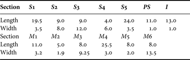
The basis of the design is the property of a narrow rectangular slot to generate linearly polarized electric field of good polarization purity. A combination of two such slots or sections of a slot placed at right angles will produce orthogonal polarizations. The proposed antenna is printed on both sides of a commercial grade FR4 substrate with the top and the bottom sides as shown in Fig. 1. On the top side is the ground plane with an L-shape slot etched on it whereas the bottom side has the microstrip feed lines. Both the L-shape slot and the feed lines are sectioned for obtaining UWB behavior. The two feed lines cross the respective slot sections orthogonally. Microstrip feed is chosen over CPW feed since it offers greater degree of freedom in design and results in less cross polarization. Although a straight feed is used to excite the vertical slot arm, a chamfered bent (L-shape) feed is used to excite the horizontal slot arm. This is done to increase the physical separation between the two feed circuits in the available antenna space and improve the isolation. The L-shape feed also improves the impedance matching. A parasitic slot (PS) is introduced to bring the reflection coefficient well below −10 dB near 8.5 GHz and a slot stub (I) is introduced to improve the isolation. Dimensions (lengths and widths) of the various sections of the slot and feed lines are given in Table 1.

Fig. 1. Proposed antenna configuration.
Table 1. Dimensions of proposed antenna (in mm).
III. RESULTS AND DISCUSSION
A) Measured and simulated S-parameters
The measured S-parameters of the proposed antenna are shown in Fig. 2 along with the simulated ones. Ultra wide impedance bandwidth with a lower edge frequency of 3.4 GHz for port 1 excitation and 3.8 GHz for port 2 excitation is noted from the S 11 and S 22 curves. The difference in the lower edge frequencies is because the two circuits are not identical.
Fig. 2. Measured and simulated S-parameters.
The presence of multiple resonances in the reflection coefficient characteristics is due to the increased number of reactive elements in the circuit. A single uniform slot is electrically a tank circuit consisting of inductance and capacitance which depend on the slot length and width. The presence of multiple sections of different lengths and widths leads to a number of such tank circuits in parallel. This increases the number of reactive elements causing multiple resonances to appear. The merging of these resonances gives the ultra wide bandwidth. A symbolic equivalent circuit of one of the arms of the proposed antenna is shown in Fig. 3. In the circuit each slot step is represented by an R–L–C circuit while the metallic short at the slot end is shown by the inductance Ls. Although the resistance “R” and inductance “L” are dependent on the length of the slot segment, the capacitance “C” will depend on the width. Similarly, the steps in the microstrip feed are represented by their R–L–G–C parameters while C o represents the open circuit capacitance at the feed end. The third step in the feed line behaves as a patch antenna and hence its radiation resistance R rad has been included in series with the R, L, G, C parameters. The coupling of electromagnetic energy from the microstrip feed to the slot is depicted by means of a transformer of turns ratio 1:n. The coupling takes place exactly at the center of the slot.
Fig. 3. Symbolic equivalent circuit for one of the arms of the proposed antenna.
The measured isolation seen from Fig. 2 varies between 20 and 30 dB in the operating region. The isolation of the proposed antenna has been improved by (1) using L-shape feed line for exciting the horizontal slot arm and (2) by inserting a slant slot stub “I” at the junction of the arms. A slant stub as proposed in [Reference Lee, Chen and Hsu5] restricts the spread of the ground plane currents and thus reduces the coupling over certain frequencies. The simulated isolation S 21 without the stub “I” is also shown in Fig. 2 (dotted green line). The maximum improvement with the stub is seen around 7.5 GHz where the stub length (13 mm) is close to λ eff/2.
The effect of the PS on S 11 is shown in Fig. 4. The S 11 of the optimized design without the PS (red line, Fig. 4) shows a peak (>−10 dB) near 8.5 GHz. The profile is corrected by the introduction of PS whose length (11 mm) is tuned to create a resonance at the correct position (8.3 GHz). The impedance matching in the neighborhood of the resonance is also improved and the overall response becomes UWB. As the length of the PS is decreased, the introduced resonance shifts upwards. The variations in S 11 with a change in the position of the PS for a fixed slot length (11 mm) are shown in Fig. 5. The resonance is seen to shift toward higher frequencies as the PS is moved away from the patch in the vertical direction or away from the slot in the horizontal direction. Further, there exists an optimal placement for obtaining the best performance. In the antenna, the feed section M3 also behaves as a microstrip fed patch placed on a defected ground. The role of the PS then is to create an additional resonance by itself (where its length l = λ/2) and to shift the resonance of the patch M3 by disturbing the ground plane currents underneath it. At a particular position of PS, when these two resonances favorably combine with the impedance behavior of the main slot, overall wideband characteristics are obtained.
Fig. 4. Effect of PS length on S 11 and S 21.
Fig. 5. Variation in S 11 with position of parasitic slot.
B) Aperture field distribution and radiation patterns
To verify the dual polarized behavior, the aperture field distribution for different port excitations is plotted at 5.7 GHz in Fig. 6. When port 1 is excited, horizontally directed electric field gets established in the vertical arm of the slot while little cross polarization is seen in the horizontal arm. The converse is true for port 2 excitation which results in vertical polarization.
Fig. 6. Aperture electric field at 5.7 GHz.
The measured and simulated radiation patterns of the proposed antenna are shown in Fig. 7. The simulated cross polarization is seen to be around −15 dB along the boresight direction over most of the frequencies. The measured cross-polarization is however higher owing to the poor characteristics of the reference horn antenna used in the measurement system.
Fig. 7. Measured and simulated radiation patterns.
IV. BAND-NOTCH DESIGN
To avoid interference of the proposed antenna with existing WLAN systems operating in the 5.1–5.85 GHz range, a band-notch is desirable in this range. The design of the proposed antenna is modified next to implement this band-notch characteristics. An impedance notch is created in the 5.1–5.9 GHz band by placing two C-shape metallic strips adjacent to the feed line. The dimensions of the strips are shown in Fig. 8. The strips placed near the two feed lines are slightly different in shape but the total length of each strip (C1 = 16 mm, C2 = 16.5 mm) is nearly equal and tuned to satisfy the condition (l = λ eff/2) for causing the notch at 5.5 GHz. As seen from Fig. 8, the C-shape strips also have slant strips at the corner. The slant strip on C1 has a length of 2.4 mm while that on C2 has a length of 1.6 mm. The purpose of introducing these strips is to suppress the harmonic tending to create an undesirable anti-resonance near 10 GHz. Further, in this design, M1-width is changed from 3.2 to 3.5 mm and S5-width is changed from 3.5 to 3.1 mm.
Fig. 8. Modified design for band-notch characteristics at WLAN.
In Fig. 9, the simulated and measured voltage standing wave ratios (VSWRs) for the band-notch design are shown along with the isolation. On comparing with Fig. 2, it is seen that the C-shape strips, apart from creating the impedance notch in the desired band, improve the isolation by an additional 10 dB in that band. A characteristic dip over the notch frequencies is also observed in the measured peak gains (shown for both the original and the band-notch versions) shown in Fig. 10. The reduction in the gain can also be seen from the radiation patterns for the band-notch design. The simulated and measured radiation patterns at one of the in-band frequencies (5.4 GHz) for the band-notch design are shown in Fig. 11. A comparison with the patterns shown in Fig. 7 can be made to appreciate the gain reduction. Finally, the variation in the center frequency of the notch band (Port 2) with the length of the C-shape strip is shown in Fig. 12.
Fig. 9. Measured and simulated performance of the band-notch design.
Fig. 10. Peak gain comparison of the antennas (with/without notch).
Fig. 11. Radiation patterns of the band-notch design at one of the in-band frequencies (5.4 GHz).
Fig. 12. Variation in the notch frequency with length “l” of C strip.
A) Envelope correlation coefficient
An important quality indicator for a two port antenna is the envelope correlation coefficient ρ e calculated using (1). A lower value of the correlation coefficient indicates less cross talk during simultaneous usage of the two ports.
 $${\rho_e} = \displaystyle{{\vert {S_{11}^\ast} {S_{12}} + S_{21}^\ast {S_{22}}{\vert ^2}} \over {(1 - (\vert {S_{11}}{\vert ^2} + \vert {S_{21}}{\vert ^2}))(1 - (\vert {S_{22}}{\vert ^2} + \vert {S_{12}}{\vert ^2}))}}.$$
The simulated and measured correlation coefficients for the proposed antenna (without notch) are shown in Fig. 13. In the same figure, the correlation coefficients for the band-notch design are also shown. It can be observed that both the simulated and measured correlation coefficients for both the antennas are almost equal and found to have low values (<0.002). The band-notch seen in the S-parameters and peak gain is seen to have little effect on the correlation coefficient as also observed in [Reference Chacko, Augustin and Denidni12] and [Reference Zhao, Zhang, Zhang and Wang15].
Fig. 13. Measured and simulated envelope correlation coefficients.
VI. CONCLUSION
An L-shape, dual polarized, UWB, slot antenna is presented and experimentally validated. The two arms of the L-shape slot are excited using two separate microstrip lines and generate orthogonally polarized electric fields. Sectioning of the slot and the feed line optimizes the impedance bandwidth which starts from 3.4/3.8 GHz and extends beyond 12 GHz. The measured isolation achieved is more than 25 dB over most of the band. The antenna has nearly omni-directional radiation patterns with a measured peak gain of 3–6 dBi in the operating band. The antenna will be useful for dual polarized applications in portable UWB communication devices.
ACKNOWLEDGEMENT
The first author acknowledges the financial support from DIAT (Deemed University), Pune, India.
 Raghupatruni Venkat Siva Ram Krishna received his Bachelor's and Master's degrees in Electrical Engineering from Nagpur University, Nagpur, India in 1998 and 2002, respectively. Presently, he is working toward his Ph.D. degree at DIAT (Deemed University), Pune, India. Prior to joining DIAT, he worked as a faculty at the Dehradun Institute of Technology, Dehradun, India. His research area concerns wideband, dual, and circularly polarized antennas.
 Raj Kumar was born on May 14, 1963 in Muzaffarnagar, UP, India. He completed his M.Sc. degree in Electronics in 1987 from the University of Meerut, Meerut, India. He was awarded M.Tech. and Ph.D. degrees in Microwaves in 1992 and 1997, respectively from the University of Delhi South Campus, New Delhi, India. He worked at CEERI, Pilani from 1993 to 1994 as a Research Associate. From May 1997 to June 1998, he worked as an Assistant Professor at Vellore College of Engineering (VIT), Vellore. He worked in DLRL (DRDO), Hyderabad as a Scientist from June 1998 to August 2002 and later on joined DIAT, Pune and worked in the Department of Electronics Engineering till September 2012. Since October 2012, he is working in ARDE, Pune. His field of interest is microwave components, antennas, electromagnetic band-gap, frequency selective surface, filters, multiplexers, power dividers, couplers, numerical techniques, and ANN for microwave circuits and antennas.
 Nagendra Kushwaha received his B.Tech. degree in Electronics and Communication from Galgotia's College of Engineering and Technology Greater Noida, UP, India in 2010. He received his M.Tech. degree in Microwave Electronics from the University of Delhi South Campus, New Delhi, India in 2012. Currently, he is with the Defence Institute of Advanced Technology, Pune, India and he is working toward his Ph.D. degree. He is a student member of IEEE. His current research includes microwave and millimeter-wave circuits, especially frequency selective surface (FSS), electromagnetic band gap (EBG), metamaterials, and printed antennas.