Introduction
A metamaterial is a new type of artificial electromagnetic (EM) material consisting of metamolecules arranged in an array of subwavelength periods. Based on the design of the unit structure and its periodic arrangement, a series of unusual EM characteristics can be obtained, such as negative refractive index [Reference Liu, Zhao, Ji and Zhou1, Reference Smith, Pendry and Wiltshire2], perfect imaging [Reference Li, Bao, Jiang, Guo, Xu, Xiong, Zhang and Yi3, Reference Molaei, Heredia-Juesas, Ghazi, Vlahakis and Martinez-Lorenzo4], and invisibility cloak [Reference Chen, Wang, Cheng, Gong, Song, Yuan and Fang5]. At present, metamaterials have been realized in different EM frequency bands, ranging from microwave to visible light [Reference Lu, Wang, Zhang, Liu, Chen, nSog and Jiang6–Reference Su, Li and Xia11].
In recent years, the design concepts of metamaterial absorbers (MAs) have received much attention in academic fields. In 2008, a perfect MA was first presented by Landy et al. [Reference Landy, Sajuyigbe, Mock, Smith and Padilla12]. Subsequently, MA design has focused on wideband absorption, polarization-insensitive and large-incident-angle stability [Reference Arsanjani, Biabanifard and Abrishamian13–Reference Luo and Cheng21]. In order to increase the absorption bandwidth [Reference Luo, Shen, Zhou, Wu, Zhou and Chen22, Reference Zhang, Huang, Pu, Song, Zhao, Wu and Luo23], several methods have been utilized. For instance, wideband absorption can be achieved by packing multiple resonance structures [Reference Luo, Hu, Qiu and Zhou24], using multilayer structures [Reference Liu, Zhong, Huang, Lv, Han and Liu25, Reference Qi and Liu26], or loading the lumped elements [Reference Assimon and Fusco14, Reference Zhao and Cheng18, Reference Yuan and Cheng27, Reference You, Zhang, Jiang, Ma, Cui and Cui28]. The absorption peak can also be widened by increasing the resistance of the resonator. In these circumstances, the EM resonance can be converted into a circuit resonance between the resonance structure and the ground plate, leading to wideband EM wave absorption.
In this work, we propose a multilayer broadband MA based on the resistive film. By combining the advantages of resistive resonance structures and multilayer concepts, the proposed absorber can offer wideband absorption and large incident angle stability. A high absorption (greater than 90%) is achieved in an ultra-wide frequency range 2.34–18.95 GHz, corresponding to a relative absorption bandwidth of 156%. Moreover, in the case of oblique incidence, when the incident angle is up to 45°, the absorptivity is greater than 80% in the frequency range 2.38–19.42 GHz in transverse electric (TE) mode. In transverse magnetic (TM) mode, the absorption is maintained above 90% in the frequency range 2.95–18.79 GHz for incident angles up to 60°. Compared with previous reports, our proposed structure has prominent oblique incidence stability and thus has the potential to be used in EM energy harvest applications.
Structure design and simulation
The designed MA structure consists of three-patterned resistance film layers, three dielectric substrate layers, and a metallic ground plate. The substrates were realized on Peek with a relative permittivity of 3.2 and a loss tangent of 0.001. The metallic ground plate is made of copper with a thickness of 0.017 mm and electric conductivity of 5.8 × 10⁷ S/m. The configuration of the unit cell structure is shown in Fig. 1 and the optimized parameters of the MA are listed in Table 1.

Fig. 1. Schematic geometry of unit cell for broadband MA. (a) Multilayer structure. (b) Bottom layer with square-modified resonator (SMR). (c) Middle layer with square ring resonator (SRR). (d) Top layer with square patch.
Table 1. Dimensions and parameters of the proposed absorber

The absorptivity can be defined as

where S 11 (ω) and S 21 (ω) are the reflection and transmission coefficients, respectively. In the simulation, S 21 (ω) is almost zero due to the existence of the metallic ground plate and thus the absorptivity is determined only by the reflectivity R (ω). Thus, the absorption can be calculated using the equation:

The simulation results were obtained using a finite-difference time-domain method. In the simulations, unit cell boundary conditions were employed in the x and y directions and the Floquet port condition was utilized in the z direction. Moreover, we use different sheet resistances to simulate different resistive films. The absorption spectrum of the absorber under the normal incidence of the TE- and TM-polarized wave is shown in Fig. 2. It can be observed that the absorption is above 0.9 in the frequency range 2.34–18.95 GHz for normal incidence. The relative absorption bandwidth W RAB of the absorber can be defined as:

where f U and f L are the high and low limits of the frequency range with an absorption above 0.9, respectively. From equation (3) it can be seen that the W RAB value of the proposed MA can reach 156%.

Fig. 2. Absorption spectrum under normal incidence of TE- and TM-polarized wave.
The normalized input impedance of the MA is defined by:

Figure 3 shows the normalized input impedance of the designed MA. From Fig. 3, it can be seen that the real part of the normalized input impedance is near unity and the imaginary part is near zero, which approximately matches the impedance of free space in the frequency range 2.34–18.95 GHz. Hence, the MA provides effective wideband absorption.
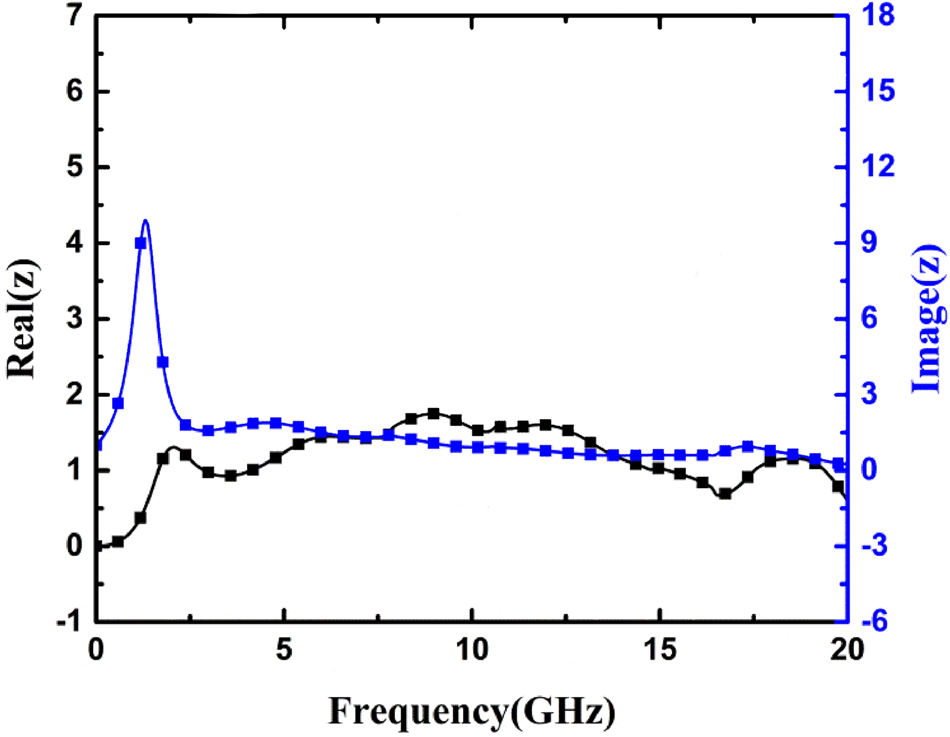
Fig. 3. Normalized input impedance of the proposed MA.
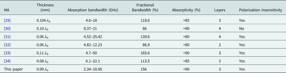
Table 2 compares the performance of the proposed absorber with some other broadband MAs that have been recently reported. As shown in Table 2, the proposed MA exhibits ultra-wideband absorption with high absorptivity. Most importantly, the lower absorption limit of the proposed MA is much lower than the other reported results, which provides a significant advantage for EM stealth.
Table 2. Performance comparison of wideband MAs, where λ 0 is the wavelength of the lowest absorption frequency

Results and discussion
Absorption mechanism
At the first stage, an equivalent circuit model (ECM) is performed to analyze the proposed structure. Figure 4 illustrates the ECM of the proposed multi-layer MA, as each resistive layer can be represented by a series Resistor-Inductance-Capacitance (RLC) circuit where Ci represents the coupling capacitance between two neighboring patches. Li and Ri represent the equivalent inductance and resistance of the resistive patch, respectively. Based on the transmission line theory, the input impedance at each layer shown in Fig. 4 can be expressed as:


Fig. 4. Equivalent circuit model of the proposed MA.
Hence, the reflection of the whole structure can be described as

where Z 0 is the wave impedance of free space. Combining equation (7) with (2), one can get the total absorption of the proposed MA.
The absorption spectra for different combinations of resonators are shown in Fig. 5 in order to facilitate a detailed explanation of the wideband absorption mechanism of the MA. Figure 5 shows that single layer SMR provides neither broadband absorption nor high absorptivity. However, by introducing another square-modified resonator (SRR) structure into the MA, a broader absorption bandwidth can be achieved due to the better impedance matching with free space at higher frequencies. Additionally, by packing a square patch into the MA, ultra-wideband absorption can be realized due to overlap between the broadened resonance peaks of the resonator as the resistance increases, ensuring a high absorption within a wide frequency range.

Fig. 5. Absorption spectra for different combinations of resonators.
The surface current distribution of each conductive layer can be plotted in order to further understand the physical mechanism of the absorption. The surface current distributions are illustrated in Fig. 6 at the resonant frequencies of 2.9, 7.1, 10.4, 15.3, and 17.5 GHz. As can be seen by comparing Fig. 6(a1) and (b1), the strongly confined surface current in the SMR is anti-parallel with that in the copper ground plate, which forms an equivalent current loop and excites a magnetic resonance at 2.9 GHz. Therefore, the excellent resonance absorption at the first peak frequency is primarily attributed to the coupling between the SMR structure and the copper ground.
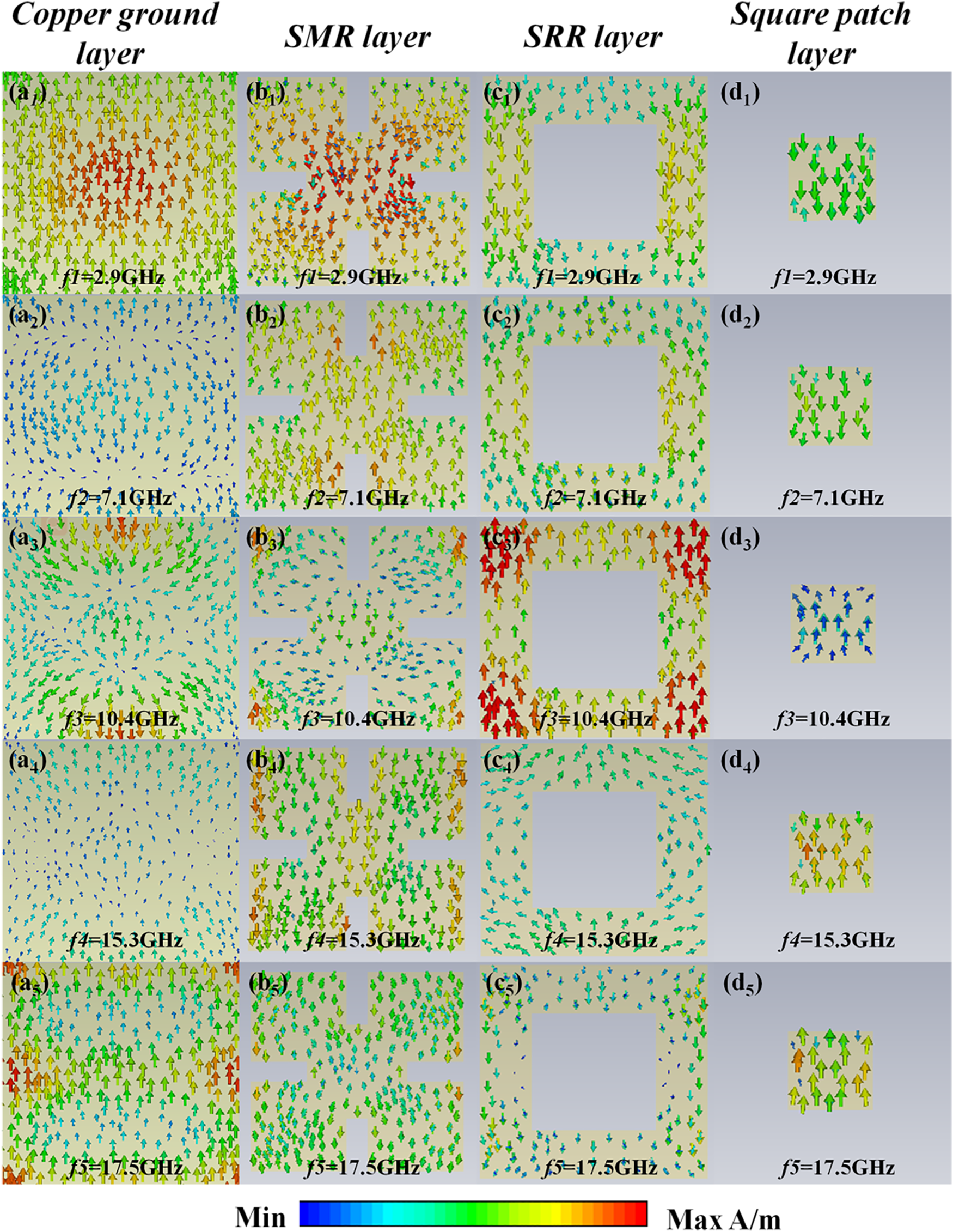
Fig. 6. Surface current distribution in (a1)–(a5) copper ground layer, (b1)–(b5) SMR layer, (c1)–(c5) SRR layer, (d1)–(d5) square patch layer at frequencies of f 1 = 2.9 GHz, f 2 = 7.1 GHz, f3 = 10.4 GHz, f 4 = 15.3 GHz, and f 5 = 17.5 GHz.
For the second resonance peak, Fig. 6(a2)–(d2) shows that the surface current distribution is mainly concentrated at the inner edges of the SMR, which means that an electric resonance is excited at the second resonance frequency. Similarly, for the third peak at 10.4 GHz, the surface current is strongly localized at the four corners of SRR, as the SRR layer plays an important role in wave absorption.
Figure 6(a4)–(d4) shows that the surface current in the SMR is anti-parallel to the surface current in the square patch, and the amplitude of the surface current in the SMR layer and top layer is higher than that of the other two layers, indicating that the absorption peak at 15.3 GHz is due to the magnetic resonance between these two layers. Finally, the fifth absorption peak at 17.5 GHz is due to both electric and magnetic resonances which contribute to the incident wave absorption. Moreover, at these resonance frequencies, there is more power consumption due to the stronger ohmic loss, which leads to a higher EM wave absorption.
Figure 7 depicts the power loss density distributions on the surface of the SMR (a1–e1), SRR (a2–e2), and square patch layers (a3–e3) at five different absorption peaks. The figures show that the power loss densities are concentrated at the edges of each resonance structure layer, where there is an intensive electric field within the absorber. Therefore, these resistive films are the main power consumer. Furthermore, as mentioned above, the power loss density of different resistive resonators varies at different absorption peaks, which indicates that a combination of multiple resonance layers can provide wideband absorption of the incident wave.

Fig. 7. Distribution of power losses in the three resistive film layers corresponding to five peak absorption frequencies: (a1)–(e1) SMR layer, (a2)–(e2) SRR layer and (a3)–(e3) square patch layer.
Absorption spectrum dependence on geometrical parameters
Figure 8 demonstrates the effect of the geometrical structure on the absorptivity of the MA. As shown in Fig. 8(a), changes in the loss tangent of the substrate have only a very slight influence on the absorption performance of the MA, which further illustrates that the dielectric layers have little effect on the energy consumption. Figure 8(b) shows the influence of the dielectric constant of the substrate which is that both the absorption bandwidth and the absorptivity decrease as the dielectric constant increases. Additionally, all absorption peaks show an obvious red-shift when the substrate dielectric constant increases from 2.2 to 4.2. Hence, by using a substrate with a smaller dielectric constant, the absorption bandwidth of the proposed MA could be further increased.

Fig. 8. Absorption spectrum dependence on (a) loss tangent, (b) dielectric constant of the dielectric substrate, (c) gap width c of SMR layer, (d) inner edge length f of SRR layer, (e) length g of square patch, surface resistance of (f) SMR R 1, (g) SRR R 2, and (h) square patch R 3.
The influence of the gap in the SMR layer (denoted by c) on the absorption spectrum is presented in Fig. 8(c). As the capacitance between each split gap is dependent on c, as c increases, the equivalent capacitance decreases. Hence, the resonant peaks shift to higher frequencies, especially for the first and second absorption peak, which originate from the SMR layer. Figure 8(d) demonstrates the effect of the inner side length of the SRR layer (denoted by f) on the absorption spectrum. As f increases, the peak absorption of the third resonance frequency decreases, since a decrease in the overall length of SRR causes a decrease in the SRR inductance and therefore the resonant intensity of the third peak decreases and the resonance frequency is blue shifted. The effect of the length of the top square patch (denoted by g) is presented in Fig. 8(e). As g increases, the highest peak absorption frequency blue shifts and thus the total absorption bandwidth increases. However, an increase in g lowers the resonant intensity as the absorptivity decreases across the whole absorption band.
The influence of the surface resistance of each resistive layer on the absorbance performance of the MA is further illustrated in (Fig 8(f)–8(h)), which shows that the surface resistance of the bottom SMR layer has the greatest influence on the incident wave absorption and that the surface resistance of the top square patch plays only a minor role in absorbing EM waves. This phenomenon can be explained by referring to the surface current distributions shown in Fig. 6 which shows that the surface current in the bottom square ring resonator (SMR) layer is much stronger than in the top square patch. Hence, the performance of the MA is more sensitive to surface resistance of the bottom SMR layer.
Absorption spectrum dependence on wave polarization and incident angle
The proposed structure is further analyzed under different wave polarizations and Fig. 9 shows the simulated absorption spectra at different polarization angles. Since the multi-layer structure is symmetrical, the angle of polarization only needs to be analyzed up to 45°. It can be seen that the absorption performance of the MA remains unchanged when the polarization angle is adjusted from 0° to 45°. Therefore, the proposed MA is insensitive to the polarization of the incident EM waves.

Fig. 9. Absorption spectrum at different wave polarization angles.
Finally, the absorption performance of the designed MA under oblique incidences has been studied. For TE polarization, as depicted in Fig. 10(a), the absorption spectrum remains almost the same for incident angles up to 30°. As the incident angle continues to increase, the absorption decreases. This is due to the fact that for TE-polarized wave, the increase of incident angle reduces the horizontal component of the electric field intensity. Therefore, the field concentration on resistive films generated by the incident electric field is gradually weakened, which leads to a decrease of EM wave absorption. However, at an incident angle of 60°, the absorptivity is still above 0.7 for frequencies above 2.38 GHz. For TM polarization, as shown in Fig. 10(b), the absorptivity remains above 0.9 for incident angles up to 60° in the frequency range 2.95–18.79 GHz. Therefore, the proposed MA has good broadband absorption performance for both TE and TM polarized waves for a wide range of incident angles under oblique incidence.

Fig. 10. Absorption spectrum at different incident angles. (a) TE-polarized wave. (b) TM-polarized wave.
Conclusion
In this work, we have presented broadband, polarization-insensitive MA based on multiple resistive film layers. The simulated results have demonstrated that the absorption of the designed MA is greater than 90% in the frequency range from 2.34 to 18.95 GHz, corresponding to a relative absorption bandwidth of 156%. The absorption mechanism has been analyzed by studying the surface current distributions and the power loss density distributions, and Ohmic losses within the multiple resistive layers play an important role in effective wideband absorption. Additionally, the effects of various geometrical structural parameters on the absorption performance were also examined. One of the most attractive features of the proposed MA is that for both TE and TM incidences, wide-incident-angle stability has been demonstrated, which is important for energy harvesting. For structure realization, one can use conductive ink to print resistive patterns, while the proposed MA can be easily integrated with screen-printing technology or inkjet-printing technology. The proposed structure is compact, effective and ultra-broadband, and is suitable for potential applications in EM stealth and shielding.
Acknowledgements
This work was supported by the National Natural Science Foundation of China under project number 61871171. We thank Mogoedit (www.mogoedit.com) for its linguistic assistance during the preparation of this manuscript.
 Guangsheng Deng was born in Chongqing, China, in 1982. He received the B.S. degree in measurement and control technology and instrument from Hefei University of Technology, in 2004. He received the Ph.D. degree in computer application technology from Hefei University of Technology, in 2014. He is currently an associate professor with Academy of Photoelectric Technology, Hefei University of Technology, Hefei, China. His main research interests include THz and optical metamaterials.
 Kun Lv was born in Anhui, China, in 1996. He received the B.S. degree in Electronic information engineering from Hefei University, in 2018. He is currently pursuing his M.S. degree in electronic and communication engineering from Hefei University of Technology. His current research interests are metamaterial absorbers.
 Hanxiao Sun was born in Anhui, China, in 1993. He received the B.S. degree in Electronic information engineering from Hefei Normal University, Hefei, China, in 2017. He is currently pursuing his M.S. degree in the electromagnetic field and microwave technology. He main research interests are metamaterial absorbers.
 Yuan Hong was born in Hubei, China, in 1981. He received the M.S. degree in electromechanical engineering from Central South University, in 2007. He is currently a senior engineer with Process and Mechanical Engineering Technology Laboratory, Space Star Technology Co., Ltd, Beijing, China. His main research interests include additive manufacturing and machine design.
 Xiaoying Zhang was born in Hebei, China, in 1988. She received the M.S. degree in mechanical engineering from Beihang University, in 2015. She is currently an engineer with Process and Mechanical Engineering Technology Laboratory, Space Star Technology Co., Ltd, Beijing, China. Her main research interests include electronic packaging technology, electronics assembly, and absorbing material.
 Zhiping Yin was born in Hunan, China, in 1980. He received his B.S. degree in electronic engineering and the Ph.D. degree in the electromagnetic field and microwave technology from the University of Science and Technology of China, Hefei, China, in 2003 and 2008, respectively. Currently, he is an associate professor of the Academy of Photoelectric Technology, Hefei University of Technology, Hefei, China. His current research interests include microwave and terahertz device, phased-array antenna, and microwave imaging radar.
 Ying Li was born in Shandong, China, in 1987. He received the B.S. degree in electronic and information engineering from University of Science and Technology of China, in 2009. He received the Ph.D. degree in electronic science and technology from University of Science and Technology of China, in 2016. He is currently an assistant researcher with Academy of Photoelectric Technology, Hefei University of Technology, Hefei, China. His main research interests include microwave and millimeter-wave devices, antennas and metamaterials.
 Jun Yang was born in Anhui, China, in 1978. He received the B.S. degree in applied physics from Anhui University, Hefei, China, and the Ph.D. degree in optoelectronic technology from University of Science and Technology of China, Hefei, China, in 2000 and 2005, respectively. He is currently an associate researcher with Academy of Photoelectric Technology, Hefei University of Technology, Hefei, China. His main research interests include active and passive THz devices and metamaterials.