Introduction
In last years, radio-frequency identification (RFID) systems have gained importance and a primary role with respect to barcode systems, mainly thanks to the second-generation (Gen.2) [1] standard: the exploitation of the backscattering principle, guaranteed by dynamically changing the load connected to the tag antenna [Reference Finkenzeller2], allows low-power consumption, and the possibility to remotely power-up the tag. However, next-generation RFID systems are expected to provide more demanding tasks, in view of our future world as an Internet of Everything with all interconnected devices[Reference Costanzo and Masotti3]: hence, RFID tags will provide not only secure identification, but also advanced functionalities, such as high-precision tags localization [Reference Zhang, Yang, Chen, Zhao, Guo and Zhang4]. Current Gen.2 RFID systems can be deployable for rough localization by exploiting different attributes of the received signal [Reference Costanzo, Masotti, Ussmueller and Weigel5], but these limited performances can be achieved in favorable line of sight conditions, only: in the presence of indoor multipath propagation, the extended localization task is not within Gen.2 RFID tags’ reach.
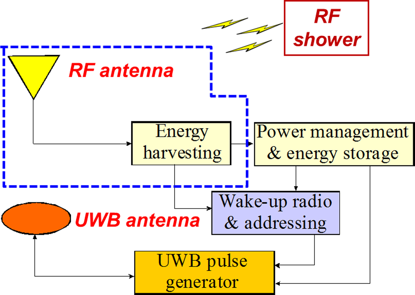
To date, the best positioning accuracy, in the order of 10–20 cm, is offered by solutions adopting the impulse radio ultra-wideband (UWB) technology [Reference Costanzo, Dardari, Aleksandravicius, Decarli, Del Prete, Fabbri, Fantuzzi, Guerra, Masotti, Pizzotti and Romani6], combined with the use of active RFID tags. In order to guarantee high-accuracy localization along with energy autonomy of tags, the combination of UWB technology with passive backscatter modulation principles [Reference Costanzo, Dardari, Aleksandravicius, Decarli, Del Prete, Fabbri, Fantuzzi, Guerra, Masotti, Pizzotti and Romani6] can pave the way to future RFID tag generation [Reference Decarli, Guerra, Guidi, Chiani, Dardari, Costanzo, Fantuzzi, Masotti, Bartoletti, Dehkordi, Conti, Romani, Tartagni, Alesii, Di Marco, Santucci, Roselli, Virili, Savazzi and Bozzi7–Reference Fabbri, Pizzotti and Romani9]. Figure 1 reports a scheme of the solution envisaged in this contribution, where besides the UWB path for communication/localization purposes, there is also a RF path for energy autonomy of the tag, through the exploitation of RF sources (“showers”) intentionally placed in the indoor ambient: with respect to more compact layouts deploying a single antenna for both the RF energy path and the UWB path [Reference Fantuzzi, Masotti and Costanzo10], a co-location of two separated antennas is preferred in this case, because the main aim of the paper is to improve as much as possible the energy harvesting capabilities. For this reason, a separated RF path for the energy collection is considered, thus guaranteeing a higher number of degrees of freedom in the dedicated design. It is also worth mentioning the possibility to deploy a less energy-hungry solution with respect to the one depicted in Fig. 1, by eliminating the on-board UWB pulse generator thanks to the exploitation of the intermodulation products generated for free by the non-linear rectifying section in case of a multi-sine RF shower [Reference Del Prete, Decarli, Masotti, Dardari and Costanzo11]: a pseudo-UWB signal can be available in this case, without loss of accuracy in the localization phase.

Fig. 1. Scheme of next-generation UWB/RF RFID tag.
This paper focuses on the possibility to energize the passive tags with battery-less techniques in the most efficient way. This goal can become very demanding if the following constraints are added to the scenario under test:
(i) indoor harsh environment, where multi-path and non-line of sight conditions easily occur;
(ii) reference nodes, acting both as UWB readers and as wireless RF power providers, are placed 10 m far from the tags;
(iii) unpredictable orientation of the tags;
(iv) maximum tag dimension 10 cm × 10 cm;
(v) a “cold start” activation is foreseen for the power management unit (PMU), placed after the rectifying antenna (rectenna).
The first two constraints put a severe limit to the expected power budget. The third and fourth ones are mainly related to the antenna design of the tag to make it compact and insensible to any rotation. As regards the last point on the dc block receiving the power rectified by the rectenna, it refers to a delicate aspect which can dramatically change the overall system performance: two different requirements are dictated by the PMU operating condition, depending on whether it is in a completely discharged (or “cold”) state or it is already accumulating energy. When designing harvesting systems, the PMU consumption in a full operation state is often addressed, thus significantly simplify the synthesis procedure. A fair design must refer to the most stringent “cold” requirement.
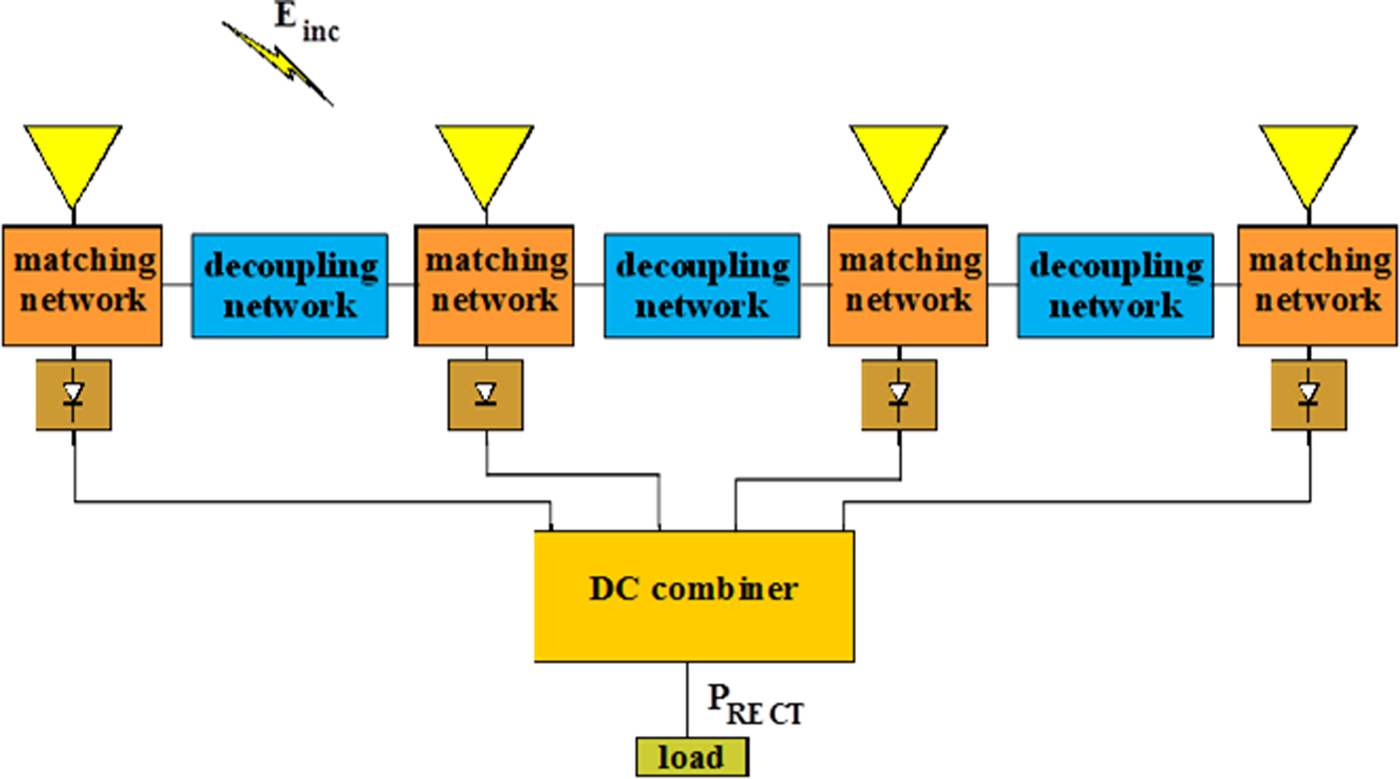
With these premises, the design of an efficient rectenna becomes mandatory, and the literature offers plenty of solutions with remarkable RF-to-dc conversion efficiencies at low-power levels in different frequency bands [Reference Niotaki, Kim, Jeong, Collado, Georgiadis and Tentzeris12, Reference Masotti, Costanzo, Del Prete and Rizzoli13]. In the present project, the selection of the RF signal to be used to wirelessly power the tags is a degree of freedom: mainly because of the 10 m source-tag distance, we select lower-range RF signals for the energization, i.e. the European Gen.2 RFID frequency band of 868 MHz. This design choice has, of course, a big impact on the harvester topology and makes the achievement of a compact layout a cumbersome task, especially if multi-antenna solutions are looked for to fight the harsh electromagnetic environment. In this case, the multi-antenna elements must be co-located in a small footprint and the unavoidable presence of electromagnetic coupling becomes a huge problem, which cannot be neglected in the design process [Reference Craeye and González-Ovejero14]. In the literature, different harvester architectures have been proposed depending on the application, i.e. dc- or RF-combination of rectennas for environmental and dedicated available RF sources, respectively [Reference Olgun, Chen and Volakis15]. In particular, when dc-combinations of rectennas, i.e. multi-antenna layouts, are involved, the close proximity of the receiving antennas can significantly deteriorate their patterns, but also cause unexpected and detrimental coupling among their ports. These effects are typically neglected in the design process and/or accepted as a cause of performance degradation in measurements [Reference Fantuzzi, Masotti and Costanzo16]. But when neat rectenna behaviors are of concern, as in the present design, it is of fundamental importance to include RF decoupling strategies aiming at avoiding destructive signal interference at the inputs of the rectifying operation. Several decoupling solutions have been proposed in the literature, mainly for MIMO applications [Reference Nadeem and Choi17]: the introduction of defected ground structures [Reference Chen and Chang18–Reference Wei, Li, Wang, Xing and Xu21], the exploitation of electromagnetic bandgap or metamaterial-based structures [Reference Assimonis, Yioultsis and Antonopoulos22–Reference Xu, Wang and Qi24], the inclusion of resonators, e.g. complementary split ring resonators [Reference Khan, Capobianco, Asif, Anagnostou, Shubair and Braaten25], or parallel coupled-line resonators [Reference Vishvaksenan, Mithra, Kalaiarasan and Raj26] represent cumbersome and not easy realizations. Simpler solutions can be those adopting neutralization lines [Reference Ou, Cai and Qian27, Reference Wang, Li and Eibert28], but they result in quite space-consuming realizations. Alternatively, simple decoupling networks can be placed in between the radiating elements, as shown in Fig. 2: these networks can be realized in planar distributed technology [Reference Khan and Warnick29, Reference Xia, Qu, Li, Jiang and Nie30] or with lumped elements [Reference Wu, Chiu and Ma31, Reference Chen, Wang and Chung32], depending on the frequency band of interest, i.e. high frequency or low frequency, respectively, because of lumped components increasing losses with frequency.

Fig. 2. Suitable block configuration for a closely-spaced rectenna array.
In this paper, the importance of the employment of the architecture of Fig. 2, firstly addressed in [Reference Fantuzzi, Masotti and Costanzo33], is demonstrated through the detailed description of the design and final realization of an orientation-independent rectenna consisting of two closely-spaced UHF monopoles (with ports closer than λ/20): because of the low RF frequency involved in the presented realization, the matching and RF-decoupling sections of Fig. 2 are combined in a simple and compact lumped-element network, whose presence allows to provide the needed dc voltage and power for powering-up a commercial PMU. The integrated circuit/electromagnetic design of the whole system is accurately described: it includes a double branch solution for each rectenna for both rectifying and waking up at extremely low-power levels. A comparison with a standard single-antenna solution demonstrates the effectiveness of the dual-antenna choice.
Single-monopole UHF rectenna
The adopted design strategies for achieving long-distance scavenging capabilities are first described through the optimization of a standard single-antenna rectenna layout able to rectify ambient energy at 868 MHz: the corresponding performance represents the lower limit the final two-monopole solution must go beyond.
The envisaged next-generation RFID tag, described by the scheme of Fig. 1, has to perform energy-consuming operations: in particular during the localization phase, when the activation of a microcontroller unit (MCU) and the consequent UWB switch modulation of the received UWB signal for the backscattering are needed. Indeed, the MCU represents the most power-hungry part of the system and strategies to keep it in an idle state for most of the time, except during the active phases, play a crucial role. To this extent, the usage of a low-power and low-latency wake-up radio (WUR) [Reference Del Prete, Costanzo, Magno, Masotti and Benini34] is adopted in this project: its purpose is to wake up the active components only when required.
Figure 3 shows the photo of the single-antenna prototype, realized on 0.5 mm-thick Rogers RO4350B substrate (ε r = 3.48, tan(δ) = 0.0037 at 10 GHz): it consists of a meandered-monopole (in order to fulfill the footprint constraint) with a zoomed view of the lumped-element matching network. The corresponding circuit schematic is reported in Fig. 4, where the two-path rectifier (consisting of a couple of voltage doublers) for both the rectifying (RECT) and the WUR operations is visible. It is worth noticing the replacement of the standard lossy resistive divider with a novel fully reactive power divider: it properly splits the received RF power into two unequal portions, in order to guarantee activation for low-power levels and, most of all, without deteriorating the main rectifying action (as verified later on), but it results an almost lossless component, except for those due to the parasitic of the non-ideal capacitors [Reference Costanzo, Dardari, Aleksandravicius, Decarli, Del Prete, Fabbri, Fantuzzi, Guerra, Masotti, Pizzotti and Romani6].

Fig. 3. Photo of a single-monopole rectenna, with a detailed view of the matching/rectifying sections.
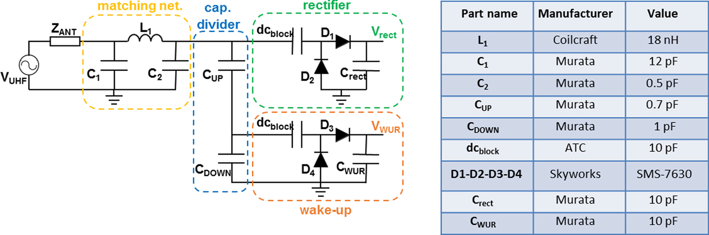
Fig. 4. Circuit schematic representation of the rectenna of Fig. 3, with components value.
As the last design choice, the ultra-low-power commercially available PMU TI BQ25570 [35], well suited for ultra-low-power applications, is placed as the load of the rectifier branch. As already stated in the Introduction, a clear distinction between the energy requirements of the “cold start” and “already active” states of this PMU must be made: to comply with its “cold start”, a dc voltage of 330 mV and a dc power of 15 µW are needed. After the critical start-up phase, this PMU is able to continue the charging operation with less strict input requirements: voltages as low as 100 mV and consumption of only 7.5 µW are sufficient. The first couple of values are adopted as a reference in the design of the presented rectifying units: as will be clearer in the following, this choice has a strong impact on the maximum operative distance of the system.
The circuital/electromagnetic co-design approach has demonstrated its effectiveness and relevance when non-linear radiating circuits are involved [Reference Costanzo, Donzelli, Masotti and Rizzoli36, Reference Masotti, Francia, Costanzo and Rizzoli37]: this strategy is adopted in the optimization of the single-monopole rectenna of Figs 3 and 4, where harmonic-balance analyses are repeated to maximize the RF-to-dc conversion efficiencies when low UHF power levels are available in the rectenna location (i.e. −20÷−10 dBm) [Reference Masotti, Costanzo, Del Prete and Rizzoli13, Reference Costanzo, Donzelli, Masotti and Rizzoli36]. The results of the optimization procedure are shown, in solid lines, in Fig. 5 in terms of open-circuit (OC) voltage at both rectifier and WUR outputs (Fig. 5(a)) and of RF-to-dc conversion efficiency and rectified voltage on the optimum load (10 kΩ in the present case) for a range of available RF power at the rectenna input wider than that one adopted in the optimization. In the same figure, the corresponding measured values are superimposed: very good agreement between measured and simulated results is obtained in all cases, except at the higher power levels, where the breakdown voltage of the Schottky diode is not providing accurate model prediction inside the circuit simulator. Figure 5(a) inspection allows a first encouraging comment on the previously mentioned design choices: the capacitive divider works in a proper manner, providing a V WUR around 20–25% of rectifier one (V RECT).
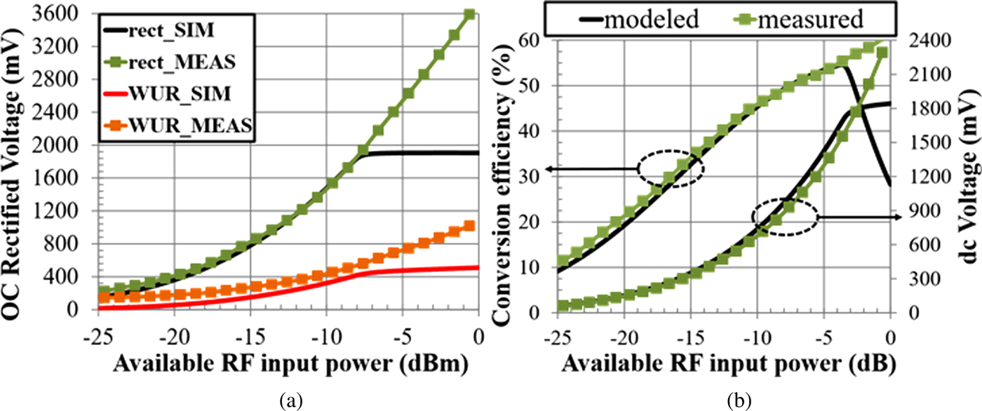
Fig. 5. (a) Open-circuit output voltage and (b) rectified voltage with RF-to-dc conversion efficiency as a function of available RF power.
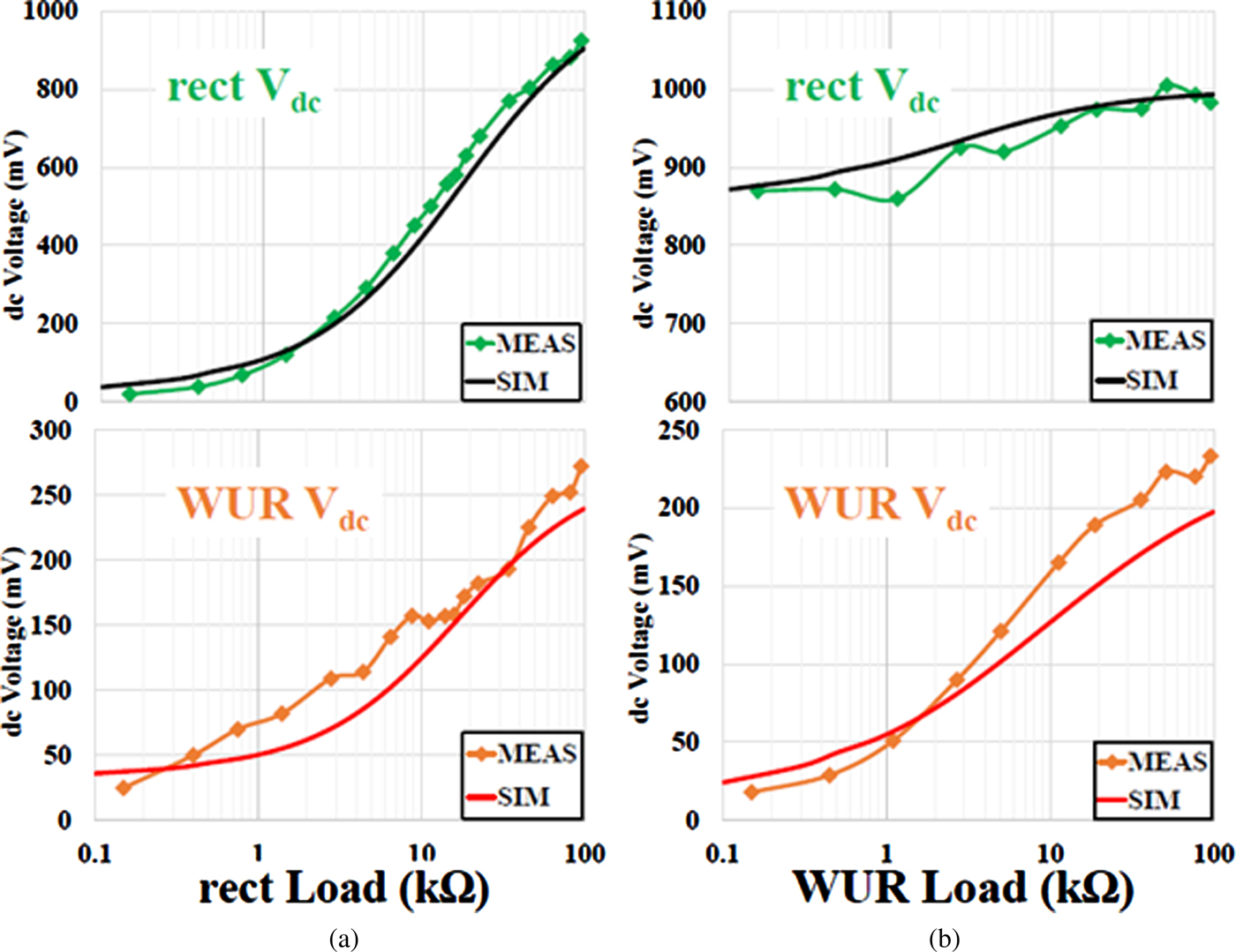
Before verifying the most stringent design constraint in terms of reference node-tag distance, the validity of the capacitive divider solution, which is able to provide a WUR implementation with no need for a dedicated antenna, has to be proven further. In order to assess the effectiveness of this solution, it is important to evaluate how the two signals might affect each other. Indeed, since the WUR is obtained from a direct derivation of the RF voltage which feeds the rectifier, a variation of the loading conditions of one signal could translate in a consequent alteration of the second one. Though the WUR alteration due to different rectifier conditions is an obvious consequence of the adopted capacitive divider implementation, the opposite case would result particularly detrimental, since the WUR should perform its operations in a seamless fashion, without affecting the main functionalities of the harvester.
The results of these proofs are shown in Fig. 6: in Fig. 6(a) the dc voltages at the RECT output port (rect Vdc) and at the WUR output port (WUR Vdc) are given as a function of the RECT load resistance. In this way, all the possible RECT operating regions (from almost OC up to almost short-circuit) are considered. The same content pertains to Fig. 6(b), where the operating region of the WUR is varied, instead. As can be evinced from Fig. 6(a) inspection, variations of the rectifier voltages reflect in direct variations of the wake-up ones, as expected, being these directly derived from the main voltage signal. If we think to the final tag usage, this is not a big concern because it does not result in fake tag activation: indeed, for almost 95% of the time, the PMU provides a constant value at the rectifier output, corresponding to the optimum loading conditions, and even though the maximum power point (MPP) tracking mechanism adopted by the PMU [Reference Costanzo, Romani, Masotti, Arbizzani and Rizzoli38] periodically refreshes its state, the refresh rate is significantly lower (few Hz) with respect to the frequency of the UHF CW modulation employed for tag addressing (in the order of kHz), therefore it is not affecting the WUR functionalities.

Fig. 6. Comparison between measured and modeled dc voltage at the rectifier and WUR outputs for different values of (a) the rectifier load and (b) the WUR load.
The more significant evaluation of the dual case is described in Fig. 6(b) by sweeping the WUR load value and comparing how this translates respectively to the rectifier and the wake-up outputs. Obviously, the voltage at the wake-up output is changed accordingly, but this variation exerts only a minor influence on the rectifier signal, as desired: in fact, the WUR will experience a variation of its operating condition during the tag usage, but must not compromise the main rectifier efficiency. The graph reported in Fig. 6 has been obtained for a fixed available power level at the input port of the circuit of Fig. 4 of −13 dBm, but equivalent conclusions are obtained all over the expected incident power range. Therefore, these results prove the effectiveness of the proposed seamless implementation of the WUR.
As regards the maximum operating distance between the UHF source and the rectenna, we refer to the optimum RF link conditions: perfect polarization matching between the linearly polarized transmitter and the receiving antenna is assumed. When 2 W ERP are provided at 10 m distance, the RF power received by the 1.8 dBi-gain monopole and made available at the harvester input is −14.3 dBm (~37.2 µW). With this received power level, the measured dc voltage is approximately 360 mV and the RF-to-dc conversion efficiency is equal to 35%, which results in a total available dc power of 13 µW. This means that, as usual, the dc voltage goal is less critical than the power one: in fact, the obtained dc voltage is able to satisfy the PMU requirements, although the dc power is still lower than the required value. Note that these measurements refer to the most favorable link conditions of perfect polarization matching. The limits of the single-monopole rectenna under examination are further emphasized by the practical need of a circularly polarized UHF transmitter for orientation independency of the RFID tag: this means a further ideal 3 dB reduction of the available RF power, resulting in measured dc voltage and power outputs of 220 mV and 5 µW.
Dual-monopole UHF rectenna with decoupling network
Because of the expected unsatisfactory results of the single-monopole solution, a more sophisticated solution is needed for the complex scenario under test.
Hence, a two-monopole layout (one vertical and one horizontal), with series dc-combination of the two rectennas output, is investigated. One can note that this solution is ideally more versatile and more efficient than the single linearly polarized antenna previously examined; but its choice is convenient with respect to a circularly polarized rectenna, too: in fact, the latter could be highly mismatched with the incoming UHF signal if inverse rotation is imposed by the tag position or by the harsh scenario.
However, the footprint constraint imposed by the indoor application (10 cm × 10 cm) forces to have highly-coupled antennas (with ports distance lower than λ/20), resulting in degradation of their radiation properties as well as signals interference due to the coupling between the antenna ports. These uncontrolled interferences could result in undesired re-radiation of a portion of the coupled signal instead of being converted to dc, as well as destructive signals power combinations: but this cannot be a priori known.
For this reason, the architecture of the two closely-spaced rectennas with dc-combined outputs of Fig. 7 has been first studied. An initial full-wave simulation of the sole linear portion of the rectenna allows to retrieve both the near-field (scattering parameters and surface currents) and far-field performance of the two-monopole assembly.

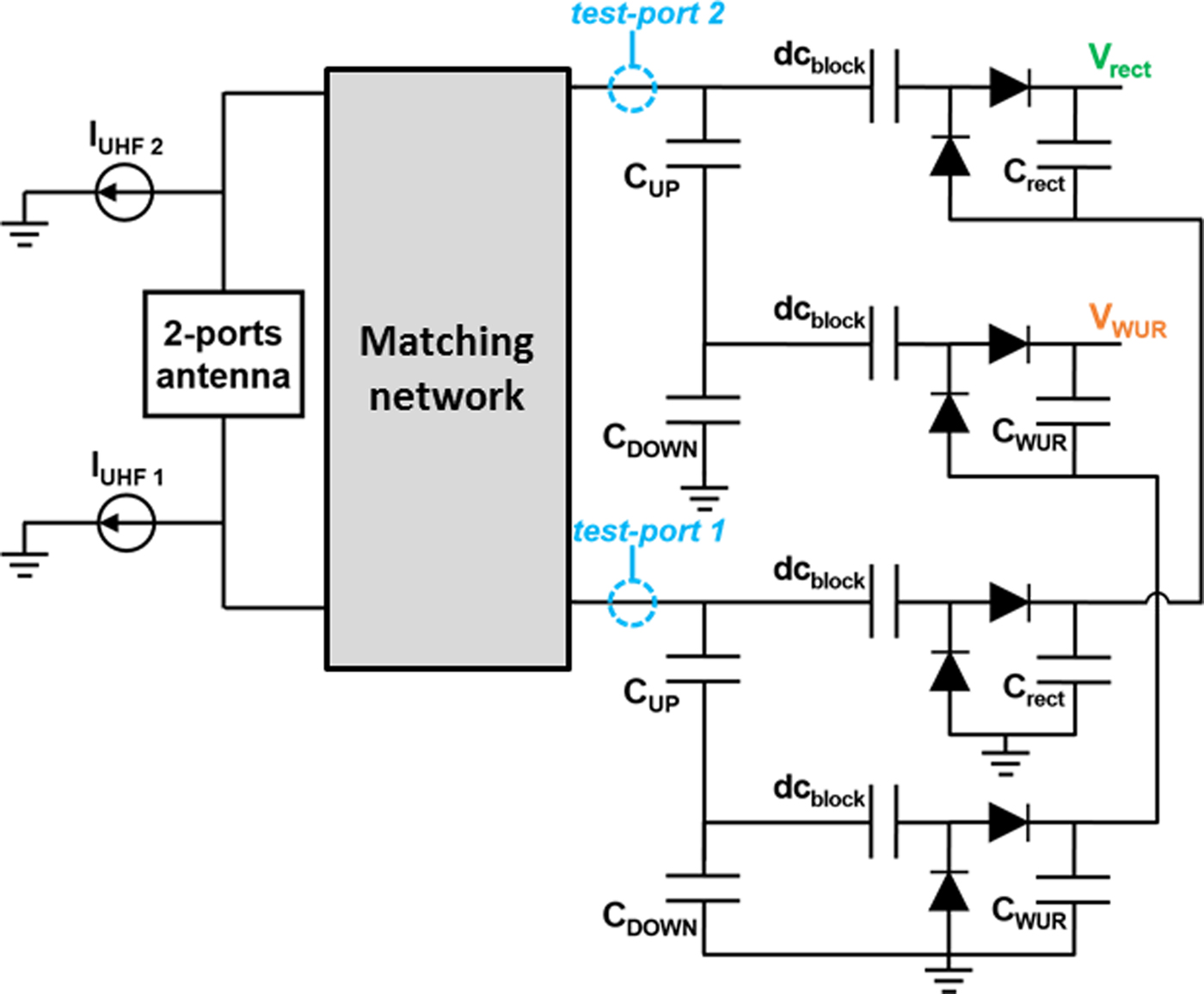
Fig. 7. Circuit schematic representation of a two-element rectenna without decoupling network.
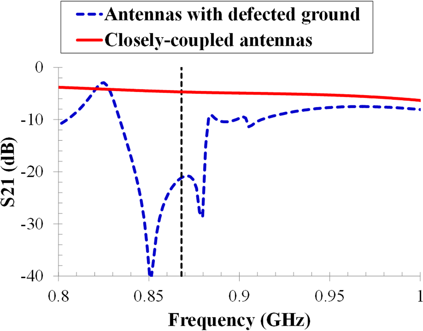
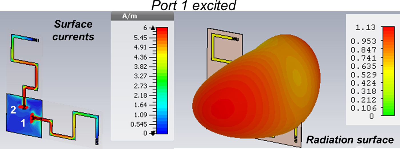
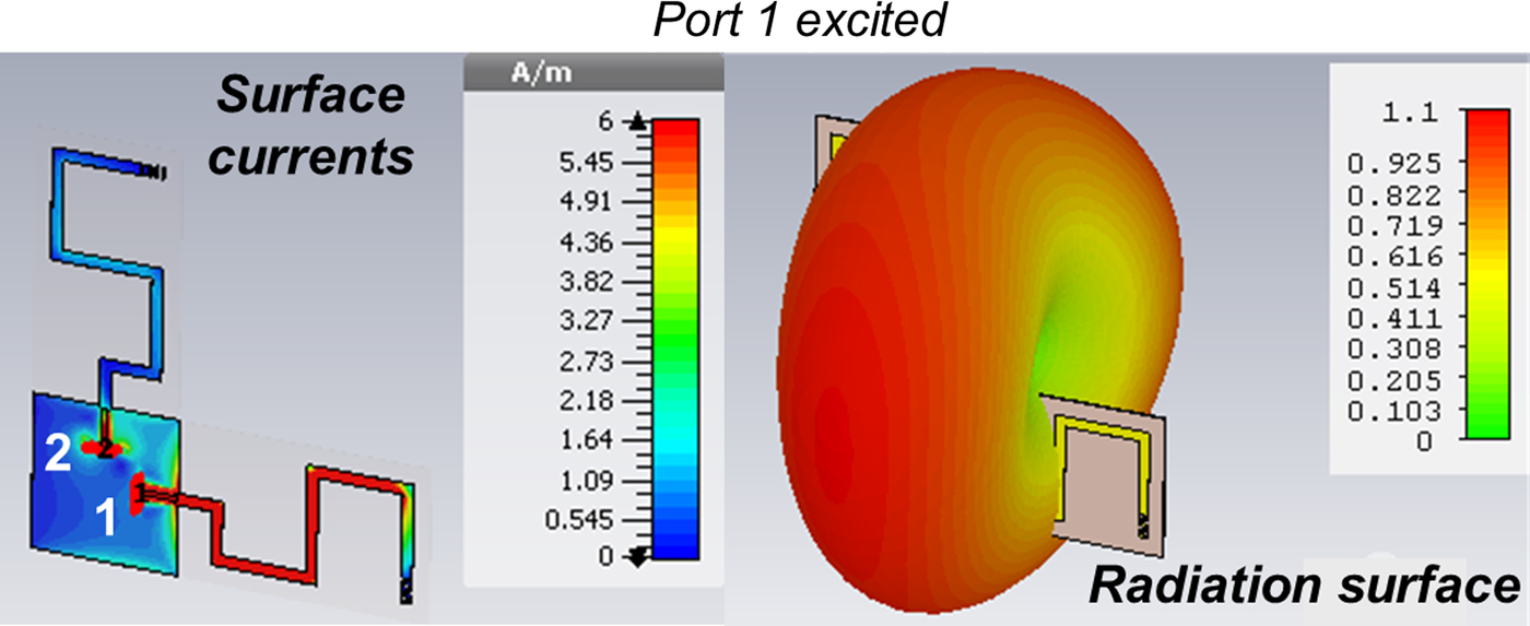
A poor transmittance value of around −5 dB is evaluated (see solid red line in Fig. 8) in the frequency band of interest. This result is confirmed by the surface current plot of Fig. 9(a), where only the metallization of the whole structure is made visible, for the sake of visualization, and port 1 (of the horizontal monopole) is excited: a strong electromagnetically induced current onto the parasitic vertical monopole is clearly visible. Finally, the radiation surface (in the same previous excitation conditions) is shown in Fig. 9(b): the presence of the unexcited vertical monopole significantly distorts the radiation mechanism, as expected by antenna theory.

Fig. 8. Modeled electromagnetic port coupling for a couple of neighboring monopoles (one vertical and one horizontal) with (dashed blue line) and without (solid red line) defected ground plane.

Fig. 9. Full-wave simulation output at 868 MHz: surface currents (left) and radiation surface (right) for two closely-spaced monopoles, when the horizontal one is fed, only.
However, one cannot a priori say if the effects of the aforementioned behavior are destructive or not, in terms of available power at the antennas port: for this reason, a more effective analysis has been carried out through the accurate evaluation of the Norton equivalent current generators at the antenna ports (see Fig. 7) (for both the single-monopole and the new two-monopole layout). The following formula [Reference Rizzoli, Costanzo and Monti39], derived by the rigorous application of the electromagnetic theory (i.e. the reciprocity theorem [Reference Harrington40]), can be adopted for this purpose:
 $$J_{eq,k}(\,f_{RF})\approx j\;\lsqb {1 + R_0Y_{kk}(\,f_{RF})} \rsqb \,\;\displaystyle{{2{\kern 1pt} \lambda _{RF}\,{\kern 1pt} r\,e^{\,j\beta r}} \over \eta} \,\;\displaystyle{{{\bi E}_{\bi i}\; \bullet {\bi E}_{\bi R}^{(k)} (\theta _L,\;\varphi _L)} \over U},$$
where E i is the incident electric field (considered as a plane wave coming from the far RF source and impinging on the phase center of the receiving antenna along the link direction (θ L,ϕ L)), E(k)R represents the field radiated by the k-th port of the receiving antenna, when it works in transmitting mode, and is driven by a sinusoidal voltage source of frequency f RF, electro-motive force U, and internal impedance R 0. Y kk(f RF) is the k-th admittance value (derived by full-wave analysis) of the multi-port receiving antenna: hence, this term automatically takes into account the effects of the transadmittance contributions (Ykp(f RF), k ≠ p) on the k-th port of interest.
The calculations carried out for both the circuits of Figs 4 and 7, for a vertically polarized incident field with 1 V/m of intensity, at a distance r = 1 m, provide the following values for the magnitude of (1): 3.8 mA for the single monopole, <1 mA at the vertical monopole input port, for the strongly electromagnetically coupled two-antenna case.
These last results suggest not to investigate further this simple two-monopole layout without any decoupling mechanism.
As a first attempt of reduction of the ports coupling, we resort to the defected ground structure reported in [Reference Chiu, Cheng, Murch and Rowell20], consisting of the removal of slits of copper from the ground plane in the region below the ports to be decoupled, with the additional need for lumped inductors in between the slits: this turns out to be a resonator whose resonant frequency is related to the distributed capacitance values among the faced slits and the inductance. Figure 10 contains both the overall view of the two monopoles with defected ground (the substrate is again made invisible) and the zoomed view of the region below the two-monopole ports: slits width is identical to slits distance and equal to 0.8 mm, whereas the (ideal) inductance value is 22 pF for all the lumped indictors. The output of the corresponding full-wave simulation in terms of transmittance magnitude is reported in Fig. 8, superimposed to that one of the previous, strongly-coupled solution: an encouraging −21 dB of the |S 21| parameter is guaranteed. Note that a de-embedding of the ports (of Fig. 10(a)) up to the slits is performed in the full-wave simulation in order to reproduce the more realistic and critical situation.
Fig. 10. (a) Layout of two closely-spaced monopoles with defected ground plane (only the metallization is made visible); (b) detail of the ground plane with slits and lumped inductors.
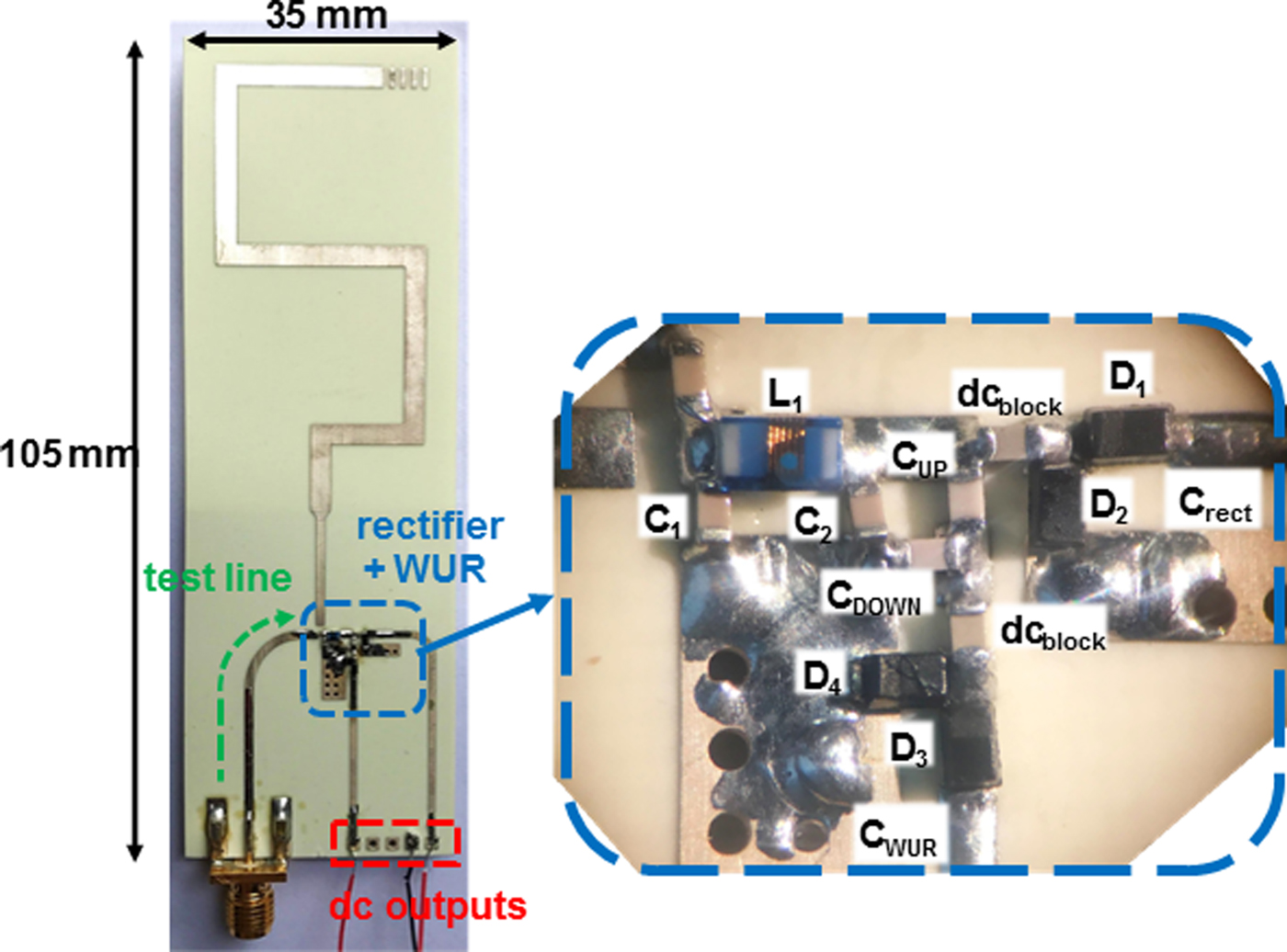
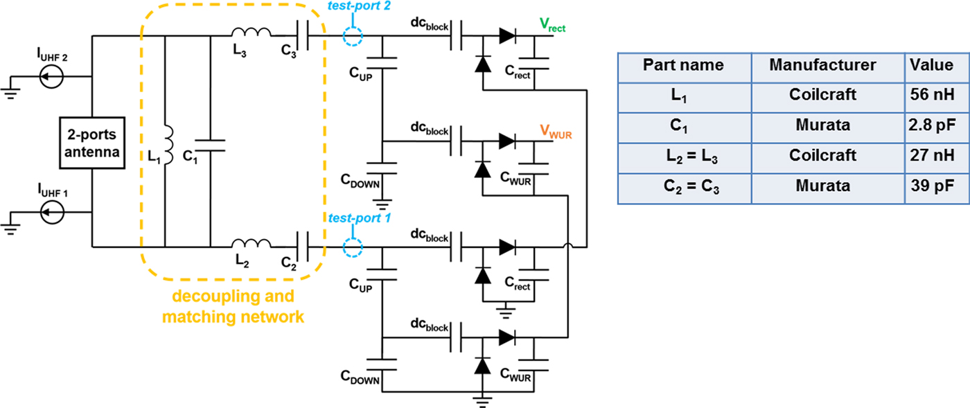
The limits of the previous solution are multiple: first of all, there is also the need of a matching network (as indicated in Fig. 7); the positioning of the inductances represents a delicate task; finally, the etching of the ground is an add-on to be included in the prototyping phase. Moreover, the replacement of the ideal inductors with real ones brings to a not negligible worsening of the decoupling behavior: the |S 21| value raises to almost −17 dB. For these reasons, we look for a simpler decoupling solution involving a limited number of lumped components, only: it needs for the proper design of a lumped-element decoupling network (similar to the one proposed in [Reference Chen, Wang and Chung32]) and working in the antennas operating bandwidth. It is worth noticing that, differently from the explicative scheme of Fig. 2, the adopted harvester layout, chosen in the present work and shown in the photo of Fig. 11 exploits a more effective unique network combining goals of both decoupling and matching. This is an additional advantage with respect to the aforementioned defected-ground architecture. The corresponding circuit schematic representation of Fig. 12 highlights the decoupling/matching network topology: it results simply composed of two parallel lumped elements and two couples of series ones, realized with SMD components.
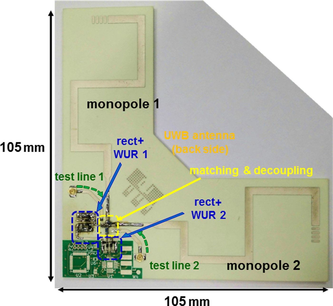
Fig. 11. Photo of the realized two-monopole prototype. The bottom-left part of the tag, containing a green solder mask, is designed for integration of the electronic components.

Fig. 12. Circuit schematic representation of a two-element rectenna with decoupling/matching network.
Of course, the output of the electromagnetic simulation of the two monopoles is adopted in the design of the circuit of Fig. 12, thus taking into account the reactive near-field frequency behavior of the unwanted array [Reference Craeye and González-Ovejero14]. To obtain the four-port decoupling network design, a two-step procedure is adopted. First, a linear analysis is carried out with the network terminated as follows: on the left-end side, the network terminations consist of the two-port, frequency-dependent Z-matrix, derived by EM-simulation, representing the two-port monopoles layout; on the right-end side, the rectifying sections input impedance of 9–j150 Ω are used, that are the capacitive divider input impedance when loaded by the rectifiers, for a receiving reference power of −13 dBm.
The results of this first approximate optimization are accounted for in the EM simulation of the resulting subsystem and are encouraging with respect to the performance without decoupling network (see Fig. 9). The corresponding results are reported in Fig. 13, where the surface currents and the radiation surface obtained by exciting port 1 (horizontal dipole) clearly show that the behavior of the horizontal dipole is almost independent of the vertical one.

Fig. 13. Full-wave simulation output at 868 MHz: surface currents (left) and radiation surface (right) for two decoupled closely-spaced monopoles, when the horizontal one is fed, only.
The equivalent Norton current generators can now be evaluated for the accurate active rectenna simulation by resorting again to (1): under the same conditions as before, the magnitude of (1) for the vertical monopole is around 4 mA (very close to the case of the single monopole), thus confirming again the results of Fig. 13 and the achievement of the design goal.
As can be evinced from Fig. 12, another design choice is worth mentioning: there are two WUR paths, one for each rectenna (both the vertical and the horizontal one), still exploiting the purely reactive divider solution. This solution is again imposed by the harsh electromagnetic environment where the tag will operate: in fact, the duplication of the double path guarantees the powering of both the WURs for any polarization of the incoming signals, thus assuring a stronger rectification (as demonstrated by the following results) starting from the initial activity. As before, the series dc connection has been realized for both the rectifier and the WUR.
A second non-linear/EM optimization is then carried out in a more rigorous way, by considering the active rectenna of Fig. 12 as a whole, for a wide range of incoming RF powers (from −20 to −10 dBm) [Reference Masotti, Costanzo, Del Prete and Rizzoli13, Reference Costanzo, Donzelli, Masotti and Rizzoli36], as for the single-monopole rectenna. The final layout of the harvester, shown in Fig. 11, foresees the inclusion of a miniaturized UWB chip antenna, according to the scheme of Fig. 1, for future UWB-based localization of the system (a proper soldering pattern is realized on the backside of the PCB).
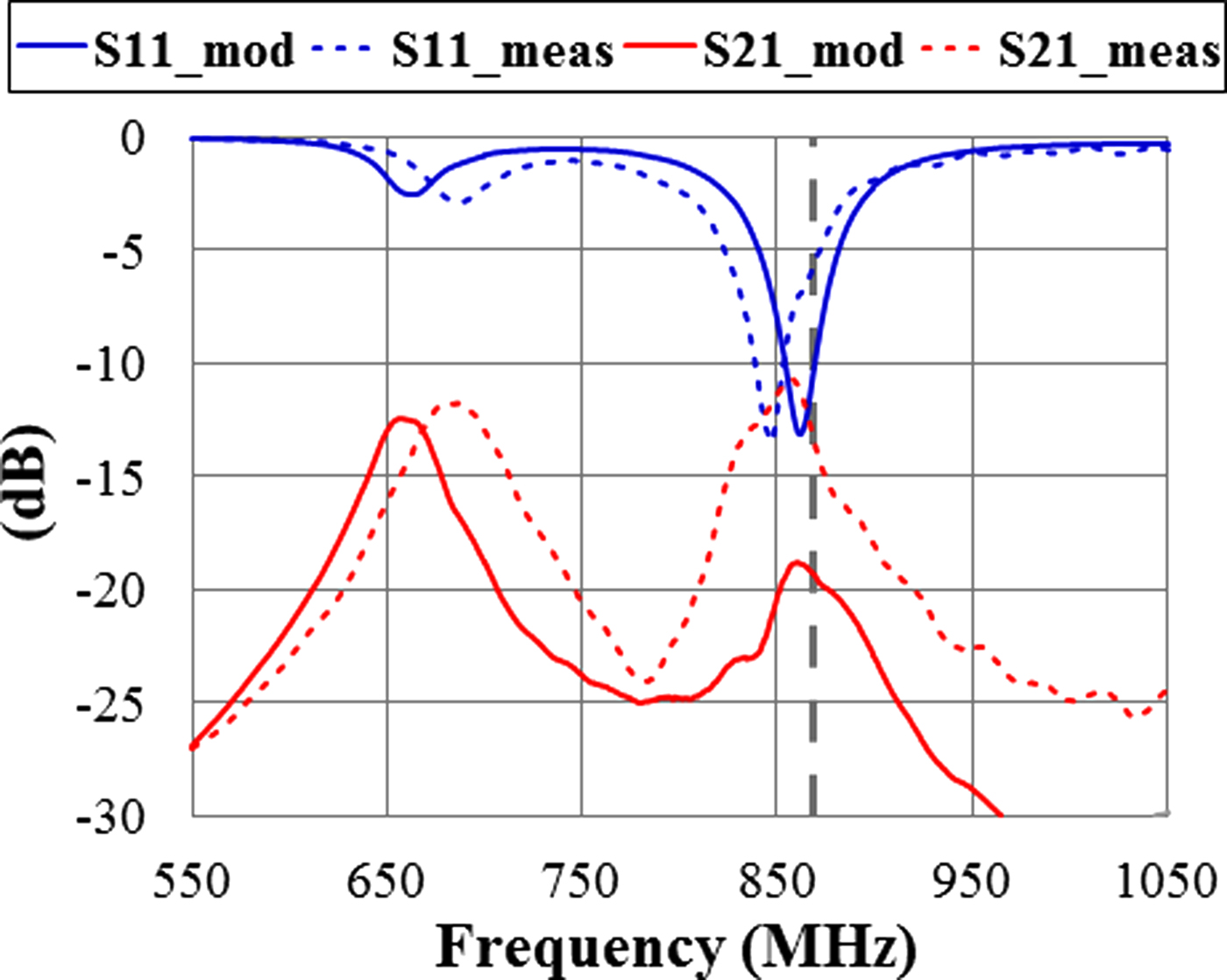
The modeled scattering parameters of Fig. 14 (solid lines), normalized again to 9–j150 Ω, provide at a glance the matching and decoupling behavior of the final topology of the network (whose element values are listed in Fig. 12): port 1 and port 2 are the additional test ports (both shown in Fig. 12 and in the prototype photo of Fig. 11) included in the final layout exactly for a separate check of the designed lumped-element network. The matching and decoupling conditions at the UHF 868 MHz frequency are satisfactory: the simulated value of the S 21 magnitude is around −20 dB, but taking into consideration the real model of the lumped components while simulating. The test lines (indicated with arrows in Fig. 12) are then exploited for the evaluation of the equivalent measured performance: the measured scattering parameters magnitudes are superimposed (with dashed lines) in Fig. 14, after a proper de-embedding of the test lines [Reference Crupi and Schreurs41] and a re-normalization of the S parameters. A good agreement is obtained between simulated and measured data, except for a small reduction of the measured decoupling, which is still below −10 dB.

Fig. 14. Comparison between the measured and modeled insertion and return loss (with sign reversal) at the two test ports, in correspondence of the interface between the decoupling network and the two rectifying sections.
The single- and the two-monopole rectennas performance is compared through a twofold test. In both cases, a circularly polarized transmitting UHF patch antenna is adopted: this choice allows a less stringent system operation, since tags should be able to rotate freely, without being restricted to predefined orientation positions. In the first part of the test, the transmitting patch antenna is kept fixed and provides an available RF power in the tag location of −13 dBm, hence each monopole (both in the single- and in the double-antenna case) receives around −16 dBm. Figure 15 shows the comparison between the two solutions in terms of rectified OC voltage and rectified power: the latter is not a direct measurement, but it is evaluated by following the operating rule of modern dc–dc converters, i.e. tracking the MPP as V RECT = V OC/2 [Reference Costanzo, Romani, Masotti, Arbizzani and Rizzoli38]; from the knowledge of this value and that one of the optimum load (10 and 15 kΩ for the single- and double-monopole rectennas, respectively), the dc power is extrapolated. This measurement/calculation is repeated for different orientation of the rectennas. As expected, each rectenna rectifies almost the same amount of power for all the orientations; however, through the two-monopole architecture, more than double rectification is achieved whatever orientation is considered.

Fig. 15. Single- and double-monopole performance for different orientations with respect to a fixed circularly polarized UHF source.
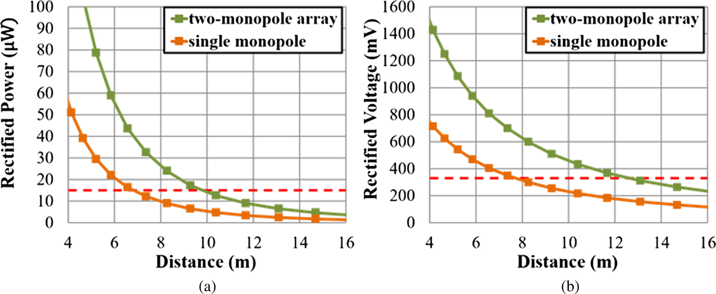
In the second phase of the test, the position of the UHF circularly polarized patch source with respect to the fixed rectennas is varied while emitting the maximum value of 2 W ERP. The measured rectified outputs are finally shown in Fig. 16: the limits imposed by the “cold start” of the adopted PMU (P DC = 15 µW, V DC = 330 mV) are reported with dashed red lines to better appreciate the fulfillment of the design goals by the advanced RF-uncoupled closely-spaced two-monopole rectenna. Hence, the effectiveness of the new rectenna array architecture and, most of all, of the achieved decoupling between the array elements is demonstrated: it ensures the stringent PMU requirements for the highest operation distance foreseen by the presented system.

Fig. 16. Comparison between single- and double-monopole rectenna for different distance from a 2 W ERP circularly polarized transmitter, in terms of (a) output dc power and (b) rectified voltage.
Conclusion
This work has demonstrated the entire design of an orientation-insensitive compact energy harvester operating at 868 MHz, which deploys two orthogonal meandered monopoles. A novel RF decoupling network is designed to avoid destructive RF interference, while keeping the antenna elements closely-spaced to comply with the overall tag reduced size. The RF power received by each antenna excites a dedicated rectifier to take advantage of the dc combination of the harvested energy, with respect to a standard single-element solution which is evident in all the operating conditions. This proposed additional network is designed together with the antenna elements and the non-linear rectifiers with the twofold goal of providing the best matching conditions, over a wide range of the rectifier regimes, and of realizing antenna–antenna decoupling, which is mandatory if a small footprint is concerned. At each output port of the RF network, a reactive unbalanced power divider is included to feed the main rectifier and a secondary one which is requested to sustain the WUR operations of the tag. The presented prototype satisfies the very strict constraints imposed by the use of next-generation RFID tags, able to guarantee autonomous UWB-based localization even in electromagnetic harsh environments.
Author ORCIDs
D. Masotti, 0000-0001-5340-2781.
Acknowledgement
This research was partly supported by the European Space Agency within the project “Localisation of Objects in Space through RF Tags (LOST)” – ESA AO 1-8471/15/NL/LvH.
 Marco Fantuzzi received the B.Sc. degree from the University of Modena and Reggio Emilia, Modena, Italy, and the M.Sc. degree (magna cum laude) from the University of Bologna, Bologna, Italy, in 2010 and 2013, respectively. He joined the Department of Electrical, Electronic and Information Engineering of the University of Bologna in 2014, where he received the Ph.D. degree in 2018. His research interests include the design of RF energy harvesting and wireless power transfer systems, as well as RFID technologies and UWB systems. Currently he is in JMA Wireless.
 Giacomo Paolini received the B.Sc. and M.Sc. degrees in Biomedical Engineering from the University of Bologna, Cesena Campus, Italy, in 2012 and 2016, respectively. He joined the Department of Electrical, Electronic and Information Engineering “G. Marconi” of the University of Bologna in 2016 as a Research Fellow within the EU-supported “HABITAT” Project. He is currently in the Department where he is working toward his Ph.D. degree. His research interests include microwave radar systems for humanitarian and biomedical applications, RFID technologies, and indoor positioning systems exploiting radiofrequencies.
 Mazen Shanawani received the bachelors in Electronics Engineering from Damascus University, Damascus, Syria, in 2000 followed by an industrial career at ZTE/Syria in Damascus as a technical engineer. He then moved to the UK and obtained the M.Sc. from the University of Bristol, UK with distinction. After that, he joined academia and worked as a laboratory instructor in Syria at the University of Kalamoon, then at the Arab International University till 2016 when he moved to Bologna to follow-up a Ph.D. program. Currently, he is working on his Ph.D. in the Millimetric and THz Rectennas Field at the University of Bologna aiming at designing an efficient rectenna system that opens up new aspects for energy harvesting in the millimetric and near visible light range. At the same time, he participates in the SINERGIE project aiming at using wireless energy transfer concepts at a wider commercial scale.
 Alessandra Costanzo is a full professor at the University of Bologna, Italy. She is currently involved in research activities dedicated to the wireless power transmission, adopting both far-field and near-field solutions, for several power levels and operating frequencies. She has authored more than 200 scientific publications on peer-reviewed international journals and conferences and several chapter books. She co-founded the EU COST action IC1301 WiPE “Wireless power transfer for sustainable electronics” where she chairs WG1: “far-field wireless power transfer”. She chairs the MTT-26 committee on wireless energy transfer and conversion. She is the AE of the IEEE Transaction on MTT, of the Cambridge International Journal of Microwave and Wireless Technologies, and of the Cambridge International Journal of WPT. She is the steering committee chair of the new IEEE Journal of RFID. She is a MTT representative and Distinguished Lecturer of the CRFID. She is an IEEE senior member.
 Diego Masotti received the Ph.D. degree in Electric Engineering from the University of Bologna, Italy, in 1997. In 1998, he joined the University of Bologna as a Research Associate of electromagnetic fields. His research interests are in the areas of non-linear microwave circuit simulation and design, with emphasis on non-linear/electromagnetic co-design of integrated radiating subsystems/systems for wireless power transfer and energy harvesting applications. He authored more than 60 scientific publications on peer-reviewed international journals and more than 100 scientific publications on proceedings of international conferences. Dr. Masotti serves in the Editorial Board of the International Journal of Antennas and Propagation, of the Cambridge journal of Wireless Power Transfer, of IEEE Access, and is a member of the Paper Review Board of the main journals of the microwave sector. He is an IEEE senior member since 2016.