Introduction
Traditional filtering mechanisms have been established based on the arrangement of inductors and capacitors. Although effective responses are achieved based on these structures, they suffer from several technical problems. Among them, rigid, non-flexible, and bulky structure, non-flexible performance, high-cost implementation, and temporal maintenance could be named. To avert these problems, significant research studies are conducted to devise techno-economic alternatives with enhanced functionalities. Frequency selective surfaces (FSSs) are defined as a combination of similar basic elements arranged in the form of array structures [Reference Munk1]. These structures are characterized with flexible response, low-cost implementation, and a wide-band operating capability. More specifically, a warm reception of FSSs is noticed in antenna and filtering design applications. Antenna radomes [Reference Zhou, Qu, Lin, Wang, Ma, Xu, Peng and Bai2, Reference Costa and Monorchio3], radar cross-section reduction [Reference Liu, Hao, Wang, Li and Gong4, Reference Jia, Liu, Wang, Li and Gong5], polarizers [Reference Orr, Goussetis, Fusco and Saenz6, Reference Euler, Fusco, Cahill and Dickie7], absorbers [Reference Li, Xiao, Bai and Wang8], and electromagnetic shielding applications [Reference Majidzadeh, Ghobadi and Nourinia9–Reference Chatterjee and Parui13] are recognized as some of the FSSs applications. As one of the main classifications, FSSs fall in two categories including single- and multi-layer structures. Single-layer FSSs are composed of one substrate layer, while multi-layer configurations include more than one substrate layer. As the number of layers increases, more resonances are excited which results in bandwidth enhancement of the proposed design. However, adoption of several layers in FSS structure not only obstructs the fabrication process but also poses economic concerns. Contrarily, single-layer FSSs are recognized with ease of fabrication and cost-effective features. Effective approaches could be perceived to enhance the operating bandwidth of these structures enabling them as apt alternatives against the multi-layer FSSs. A relevant literature review unveils that less attention has been paid on extending the state-of-the-art of wide-band single-layer FSS structures. Aiming at further improvements on these structures introduces a more important research field to be explored.
Contributing to the outlined context, this manuscript develops a new design of wide-band single-layer FSS structure with enhanced technical and operational features. The proposed unit cell is printed on 10 mm × 10 mm FR4 substrate with a permittivity of 4.4, loss tangent of 0.018, and thickness of 1.6 mm. The FSS unit-cell dimensions are smaller compared with similar previous designs which yield a cost-effective production. On the top side of the substrate, a simple circular loop is launched. Moreover, a circular loop, two perpendicular arms, and a square-shaped element are implanted on the backside to form the conductive element. These inclusions provoke the rejection of frequency band extended from 6.3 to 16.3 GHz. Such a wide-band filtering mechanism through a single-layer FSS stands as a superior technical achievement. Shedding lights on the main contributions of the proposed design, the followings could be listed:
• A compact unit cell with a simple design process is attained as a cost-effective solution,
• Extension of the proposed unit cell to a single-layer FSS structure grants a wide-band rejection capability,
• The proposed structure affords a stable response against different angles of incidence for both TE and TM polarizations. Thus, a technically approved performance is reflected.
Detailed simulation and measurement studies are conducted to assess performance of the proposed FSS. Results are discussed in terms of wide-band rejection enhancement.
The remainder of this manuscript is organized as follows. First, design steps and bandwidth enhancement process of the proposed FSS unit cell is discussed in detail. In the sequel, FSS performance analysis based on surface current distribution is presented. Next, a set of angular and polarization stability analysis is conducted on the proposed design against different polarizations and incident wave angles. Moreover, fabrication prototype and measurement results are discussed to validate the anticipated performance in real-world implementations. Obtained advantages of the proposed design with respect to similar designs are highlighted. Eventually, the concluding remarks are provided last section.
Design process of the proposed FSS unit cell
Figure 1 displays the FSS unit-cell structure. As can be seen, the unit cell is printed on 10 mm × 10 mm FR4 substrate with thickness of 1.6 mm. A simple circular loop is adopted on the top side of the substrate. Inner and outer radii are 4.2 and 4.5 mm, respectively. Another circular loop with inner radius of 3.5 mm and outer radius of 4.5 mm is printed on the backside. As can be seen, the outer radii of both top side and backside loops are equal in size. A simple square conductive element with the size of 3.5 mm × 3.5 mm is also placed at the center of the backside loop. Two perpendicular arms with 0.5 mm width are also attached to the backside loop. Evidently, the overall structure is composed of simple conductive elements on one single substrate layer.

Fig. 1. Configuration of the proposed unit cell.
To provide a comprehensive analysis, the design process of the proposed FSS is tailored in four steps shown in Fig. 2. In step 1, only a simple circular ring element is adopted on the top layer of the substrate. This element falls in “loop-type elements” category [Reference Munk1]. It is a well-known fact that these types of elements act as band stop filters wherein the rejected band is proportional to their circumference [Reference Munk1]. Herein, to make a resonance around 7 GHz, the front side circular ring with inner and outer radii of 4.2 and 4.5 mm is adopted. Results are demonstrated in Fig. 3. It can be seen that engraving one circular loop on the top side of the substrate, which excites a resonance around 7 GHz, results in the rejection of 5.8–8.2 GHz. It will be shown that by changing the radii of the loop, the resonance frequency would shift to lower or higher frequencies. To have a wide rejected band, it is necessary to tune the excited resonances in such a way with respect to each other that they do not split the rejected band into two or more bands. This is the reason of choosing the radii of the loop to be 4.2 and 4.5 mm and tuning the resonance frequency around 7 GHz. In the next step, a plate-type element in the form of a square element is placed at the center of the unit cell on substrate backside. Addition of this element is to have another resonance at higher frequencies. Excitation of resonance at high frequencies is in line with obtaining a wide-band operation. Accordingly, the inclusion of this element excites a resonance at about 19 GHz; besides, frequency ranges of 6–8 GHz and 18.5–19 GHz are stopped. Next, another circular ring is embedded on backside with inner and outer radii of 3.5 and 4.5 mm. It is obvious that due to different radii values, the resonance of this loop would differ from the top side one. In this case, the backside loop creates a resonance around 9 GHz. Evidently, the resonance of the top side loop is slightly moved toward lower frequencies due to the coupling effects between top and backside conductive elements. This configuration rejects the frequency band of 6–10.4 GHz. With the aim of further widening the rejected bandwidth, the separate elements on backside namely the square and circular ring-shaped elements are connected to each other via four arms to finalize the proposed unit-cell configuration. In this way, by changing the elements circumference and providing longer paths for the current to flow, another resonance is excited at 14 GHz which extends the bandwidth. The rejected band is extended from 6.3 to 16.3 GHz.

Fig. 2. Design steps of the proposed FSS unit cell.

Fig. 3. S 21 curves for the four-design steps of the proposed FSS unit cell.
Parametric study
It was mentioned that the radii of the circular ring element are important parameters in determining the resonance frequency. To shed light on this issue, a parametric study is carried out. Radii of the backside circular loop are named as R 1 and R 2. As it was shown in Fig. 1, R 2 is set to be 4.5 mm and R 1 is 3.5 mm which gives a difference of 1 mm. For different R 1 and R 2 values and their relevant differences, S 21 curves are plotted in Fig. 4. It is seen that by increasing the radii difference, the resonance frequency is shifted toward higher frequencies. When the difference in R 2 and R 1 reaches to values more than 1 mm, a gap is appeared around 7 GHz. Hence, the widest bandwidth is obtained for R 2 − R 1 = 1 mm.

Fig. 4. S 21 curves for different values of R 1 and R 2.
Substrate is one of the most effective and important parts of every FSS. Hence, its parameters directly influence the FSS performance. Herein, to assess the FSS performance against different substrate materials with different relative dielectric constant, three materials are selected as RT Duroid 5880 with relative dielectric value of 2.2, FR4 with relative dielectric values of 4.4, and RT Duroid RO6006 with relative dielectric value of 6.15 and corresponding simulated results are plotted in Fig. 5. It is clearly seen that by increasing dielectric constant, resonances are excited in lower frequencies. This behavior is due to the fact that the resonance is inversely proportional to square root of dielectric constant.

Fig. 5. S 21 curves for different substrate dielectric constant.
Surface current distribution analysis
To assess the FSS performance in more detail, surface current distribution is studied in this section. As it is well known, surface current distribution analysis is a powerful tool in analyzing the overall performance of FSSs. Figure 6 shows surface current concentration at resonance frequencies of 6.5 and 14 GHz. As the color bar indicates, the colors tending to red indicate stronger current. However, current color with a tendency toward blue means weaker current concentration on FSS unit cell. The results clearly indicate that in 6.5 GHz, due to the current concentration on the circular ring on the backside of the substrate, this element is responsible for the resonance excitation. As well, in 14 GHz, parts of the front side conductive element as well as the backside element radiate effectively to excite a resonance at this frequency.

Fig. 6. Surface current distribution on the FSS unit cell.
Angular and polarization stability analysis
In filtering applications, a FSS structure might be subjected to various waves with different incident angles and polarizations. In these situations, a properly designed FSS should provide a stable performance, i.e. being less affected by the environmental conditions [Reference Simovski, de Maagt and Melchakova14–Reference Luukkonen, Costa, Simovski, Monorchio and Tretyakov16]. To assess the functionality of the proposed FSS, two TE and TM polarizations are explored individually. These polarizations are tailored at different incident θ and φ angles from 0 to 50° with step of 10. Results are demonstrated in Figs 7 and 8 for θ variation and Figs 9 and 10 for φ variation. Results in Figs 7 and 8 indicate that for angles up to 30°, almost stable response is obtained. For θ angles more than 30°, some reduction is seen in bandwidth. To have a precise view of the matter, Table 1 reports the percentage of bandwidth reduction for different θ angles. For θ = 40°, the bandwidth reduction is about 31% with respect to the bandwidth obtained for θ = 0°. This reduction value is 42% for θ = 50°. Better stability is obtained for φ angle variation as shown in Figs 9 and 10. It can be clearly seen that in both of the polarizations, the overall performance remains almost constant. The resonance frequency positions as well as the rejected frequency range are almost the same for different incident angles. In fact, no variation with respect to φ angle can be seen due to the symmetry of the scattered pattern. Generally speaking, the proposed FSS exhibit acceptable performance in different θ and φ angles and could be suitably utilized in communication systems.

Fig. 7. S 21 curves for different θ angles of TE polarization.

Fig. 8. S 21 curves for different θ angles of TM polarization.

Fig. 9. S 21 curves for different φ angles of TE polarization.

Fig. 10. S 21 curves for different φ angles of TM polarization.
Table 1. Bandwidth reduction percentage in different θ angles for TE and TM polarization

Measurement results and analysis
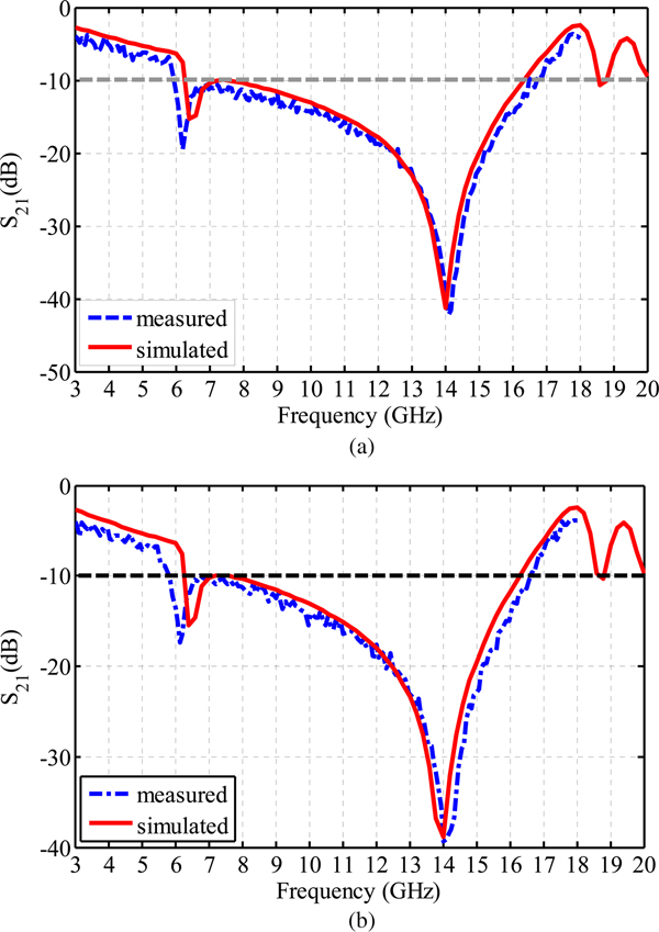
To analyze the performance of the proposed FSS in real-world applications and validate the simulation results, an experimental prototype is fabricated and measured in antenna and microwave laboratory. The fabricated prototype is shown in Fig. 11. This structure is printed on 200 mm × 200 mm × 1.6 mm FR4 substrate which is composed of 400 unit cells. In measurement set-up, two wide-band horn antennas are deployed as transmitter and receiver. The transmitter horn illuminates signal with wide frequency range of 2–18 GHz toward the FSS screen. On the other side of the FSS, the receiver horn welcomes the signal which is passed the FSS. Technically speaking, the signals with frequencies within the FSS pass band could find the opportunity to pass the FSS. Whereas, the others are stopped within the FSS rejection band. Figure 12 demonstrates the established set-up in measurement process. The fabricated FSS is placed between the transmitter and receiver horn antennas both of which are connected to the network analyzer to display the corresponding waves. By this way, the measured and simulated S 21 curves could be explored. Results are demonstrated in Fig. 13. As can be seen, a close agreement is confirmed between the simulated and measured results on both TE and TM modes. Accordingly, the outperformance of the proposed FSS is corroborated.
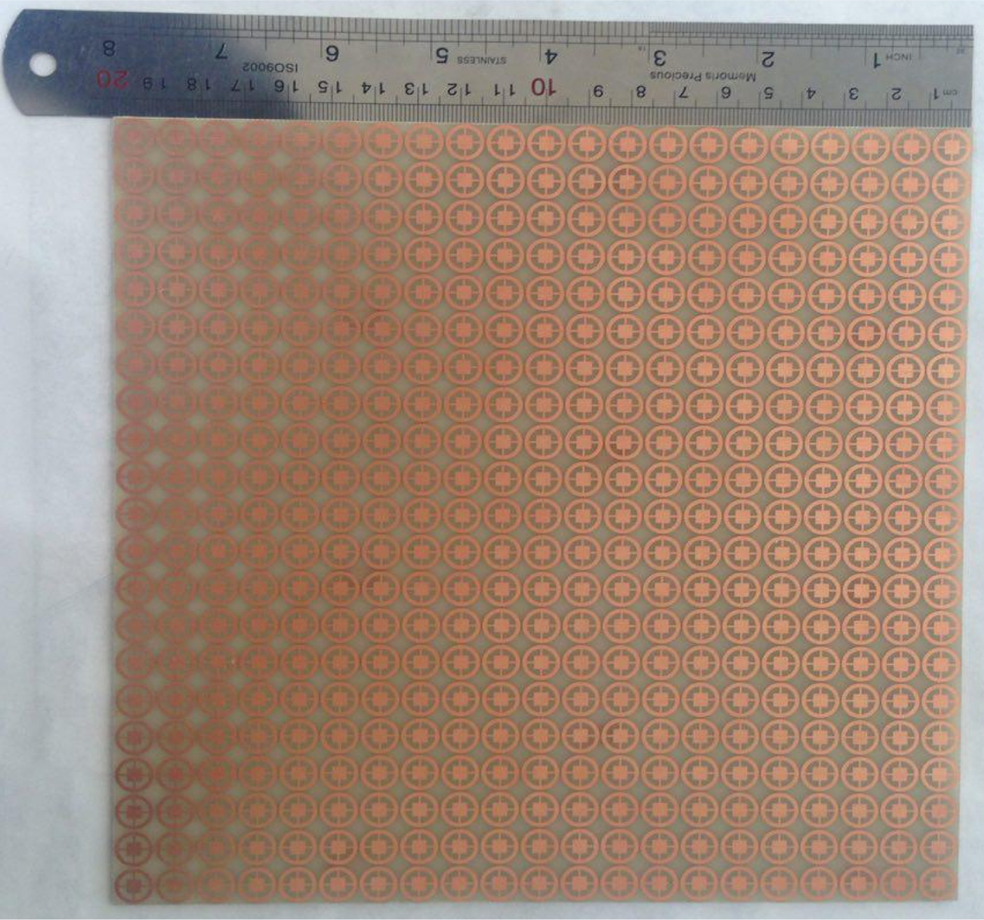
Fig. 11. Photo of the fabricated prototype.

Fig. 12. Measurement setup in antenna and microwave laboratory.

Fig. 13. Simulated and measured S 21 curves for the proposed FSS (a) TE polarization, (b) TM polarization.
Comparison with other designs
A complete study is established here to investigate the advantages of the proposed FSS with respect to the other FSS structures presented in the literature. To this aim, the present FSS structure is compared with the FSSs in [Reference Chatterjee and Parui13] and [Reference Sivasamy, Moorthy, Kanagasabai, George, Lawrance and Rajendran17–Reference Ranga, Matekovits, Esselle and Weily20]. The comparison points include FSS unit cell size, number of substrate and conductive layers, and operating bandwidth. Summary of the aforementioned structural and operational characteristics are surveyed in Table II. As this table reports, the FSS unit cells in [Reference Chatterjee and Parui13, Reference Sivasamy, Moorthy, Kanagasabai, George, Lawrance and Rajendran17, Reference Syed, Ranga, Matekovits, Esselle and Hay19], and [Reference Ranga, Matekovits, Esselle and Weily20] have larger dimensions with respect to the unit cell in this paper. This is while; they provide lower 10-dB bandwidth. As well, the FSS unit cell structure in [Reference Hashemi and Abdolali18] is smaller than the unit cell in the present work; however, it is composed of three substrate layers which makes it a bit thicker. In addition, lower 10-dB bandwidth is provided by the aforementioned structure. The presented unit cell in this paper has overall size of 10 mm × 10 mm × 1.6 mm and operates over the 10-dB impedance bandwidth of 6.3–16.3 GHz. The obtained performance is suitable to be used in communication filtering applications and systems.
Table 2. Summary of structural and operational characteristics of the FSS unit cell in this work and some previously designed structure

Conclusion
A new scheme of wide-band single-layer simple FSS was designed and explored in this paper. Judicial placement of conductive elements in the FSS configuration resulted in the rejection of wide frequency range extended from 6.4 to 16 GHz. As noticed, this performance was achieved within four design steps. In first step, inclusion of a simple circular loop on front side of the proposed unit cell provoked a rejection band of 5.8–8.2 GHz. The obtained stop band was then extended to 6–8 GHz and 18.5–19 GHz in the second step, emanated by a square conductive element stamped on the backside. As well, in step 3, backside square is located on the substrate backside which excited another resonance in the vicinity of 6–10.4 GHz. The final response, say as 6.3–16.3 GHz, was attained due to the attachment of perpendicular arms to the backside element. These structural modifications resulted in the wide-band rejection by exciting different resonances. Besides, radiating different incident waves on the proposed FSS unveiled a stable response against the environmental variations. These remarks were also certified through a fabricated prototype being measured in the antenna laboratory. Accordingly, the proposed FSS was attested as a suitable choice in related communication applications.
 M. Bashiri was born in 1983. She received her B.Sc. degree in Communication Engineering from Islamic Azad University, Urmia branch, Urmia, Iran, in 2005 and M.Sc. degrees in Communication Engineering from Islamic Azad University, Tehran South Branch, Tehran, Iran, in 2010. Now, she is a Ph.D. candidate of communication engineering at Urmia University, Urmia, Iran. Her research interests include frequency selective surface, and antenna design.
 Ch. Ghobadi was born in June, 1960 in Iran. He received his B.Sc. in Electrical Engineering Electronics and M.Sc. degrees in Electrical Engineering Telecommunication from Isfahan University of Technology, Isfahan, Iran and Ph.D. degree in Electrical-Telecommunication from University of Bath, Bath, UK in 1998. From 1998 he was an Assistant Professor and now he is a Professor in the Department of Electrical Engineering of Urmia University, Urmia, Iran. His primary research interests are in antenna design, radar, and adoptive filters.
 J. Nourinia received his B.Sc. in Electrical and Electronic Engineering from Shiraz University and M.Sc. degree in Electrical and Telecommunication Engineering from Iran University of Science and Technology, and Ph.D. degree in Electrical and Telecommunication from University of Science and Technology, Tehran Iran in 2000. From 2000, he was an Assistant Professor and now he is a Professor in the Department of Electrical Engineering of Urmia University, Urmia, Iran. His primary research interests are in antenna design, numerical methods in electromagnetic, microwave circuits.
 M. Majidzadeh was born on 18 September 1987 in Urmia, Iran. She received her Ph.D. and M.Sc. degrees in Communication Engineering from Urmia University in 2016 and 2012 and B.Sc. degree in Electronics Engineering at 2009 from the same university. Now she is an Assistant Professor in the Department of Electrical and Computer Engineering, Urmia Girls Faculty, West Azarbaijan branch, Technical and Vocational University (TVU), Urmia, Iran. Her research interests are in electromagnetic compatibility, frequency selective surfaces, designing of UWB antenna, bandwidth enhancement and antenna miniaturization techniques, circularly polarized antennas and numerical method in electromagnetics.