I. INTRODUCTION
Today's mobile radio communication is characterized by a coexistence of various different communication standards like GSM (second generation of mobile communication), UMTS (third generation of mobile communication), and its potential successor LTE (Long Term Evolution) which will be commercially introduced in near future. These standards exist in different frequency bands distributed in the L- and S-band between approximately 400 MHz up to 4 GHz. The standards have been developed and introduced in order to enable the continuously increasing data rates being necessary to support multimedia applications and mobile internet. UMTS and LTE use complex modulation schemes with non-constant envelopes, characterized by signals exhibiting a high peak-to-average-ratio of e.g. >10 dB and imposing high linearity constraints. When using classical amplifier designs, compliance with these constraints can only be achieved at the expense of power amplifier (PA) efficiency.
In order to afford today's and future mobile radio applications and to increase PA efficiency as well as to enable multiband and multistandard capable solutions like software-defined radio, suitable PA semiconductor technologies enabling performance improvement and supporting new promising circuit concepts are urgently required.
Against this background, Alcatel-Lucent started at an early point in time to evaluate the promising AlGaN/GaN semiconductor technology for future mobile radio PA applications within four national funded projects (GANGLION & ErGaN (2003–2006) and ELBA & Class-S (2006–2009)).
In the following sections, the progress on linear single- and multiband PAs based on AlGaN/GaN semiconductor technology provided by FhG-IAF Freiburg is described and illustrated by selected demonstrators and related characteristic measurement results. The progress has been achieved during a period of six years within GANGLION and ELBA project.
II. GANGLION PROJECT – GaN-BASED MULTIBAND PAs
Main target of GANGLION project was to evaluate the GaN technology for multiband RF PAs featuring a total covered bandwidth of up to 900 MHz and output power levels under UMTS operation of 10 W average and even higher.
A) Basic design considerations
Using established technologies like LDMOS, multiband amplifier design becomes very difficult, especially for high power levels, e.g. due to low impedance levels and thus required internal prematching. Owing to the high power density of GaN high electron mobility transistors (HEMT) devices, GaN technology brings additional possibilities and advantages for the design of amplifiers, especially for wide- and multiband amplifiers. Because to this fact, GaN HEMTs are the best choice when realizing future multiband capable amplifiers and evaluating the limits. In order to support the multiband amplifier design, which requires optimized tuning as well as appropriate parameter trade-off (e.g. gain versus efficiency and power) for different frequencies within the targeted bandwidth, CAD tools and accurate transistor models are essential. Furthermore, different important requirements e.g. coming from the communication standard (e.g. adjacent channel leackage ratio (ACLR)), from the standard related signal (e.g. Peak-to-Average Ratio (PAR)), from the targeted application (output power, frequency range, etc.) and last but not least from the chosen amplifier concept and use of linearization and reduction of signal dynamic, have to be considered when designing mobile radio amplifiers. Based on this background, the following described amplifier demonstrators have been designed.
B) First multiband capable amplifier
At the beginning of GANGLION project, a first class-AB-based PA was realized, yielding up to approx. 34 dBm peak output power when using a single-carrier W-CDMA signal. This amplifier was based on a power cell with a gate width of W G = 2 mm. Figure 1 shows a photo of the realized demonstrator and Fig. 2 the related measured small-signal S21 frequency characteristic. The amplifier exhibited a total gain of approximately 15 dB with a gain ripple of about 2 dB in the frequency range between 1.8 and 2.7 GHz.

Fig. 1. Photos of an early GANGLION multiband PA and of a packaged W G = 2 mm power cell.

Fig. 2. Measured frequency characteristic of first GANGLION amplifier.
This multiband amplifier mainly represents the status of technology and multiband RF amplifier design at the beginning of the project. Pushing forward to higher power levels, larger power cells had to be realized and challenges like stability and suitable assembly/packaging technology as well as reliable modeling of transistor and package, respectively, had to be faced.
C) Two-stage traveling-wave amplifier (TWA)
The realization of a two-stage TWA, covering a frequency range from 1.4 to 2.5 GHz was a next important step toward increased output power [Reference Wiegner2]. The TWA concept has been chosen due to the fact that it is very suited for wideband/multiband applications. The two-stage TWA shown in Fig. 3 consists of a driver stage with a gate width of W GS1 = 4 mm and a final stage with an all in all gate width of W GS2 = 16 mm, realized by two W G = 8 mm power cells each in a separate package. After the driver stage, the input power is time delayed fed into the parallel transistors. In order to compensate for this time delay, an equal delay line at the output is necessary. For power combining, a Wilkinson configuration was chosen for the TWA final amplifier stage. On the right-hand side Fig. 3 shows a photo of the employed W G = 8 mm power cell, which has been realized by combination of four W G = 2 mm sub cells. Later on inserted lumped resistors guarantee for stability by stabilizing the sub-cells against each other. This procedure resulted in a stable TWA.

Fig. 3. Photo of the two-stage TWA and of a W G = 8 mm packaged power cell.
Figure 4 gives the peak and average output power as well as the gain for the TWA module between 1.3 and 2.5 GHz. We observed a 3 dB bandwidth of 1.15 GHz between 1.35 and 2.5 GHz. The ACLR requirements at 5 and 10 MHz offset are met from 1.55 to 2.5 GHz when using a single-carrier W-CDMA signal with 10.5 dB PAR without using digital predistortion. The corresponding measured peak power is clearly beyond 40 dBm with a maximum of 43.2 dBm at 2.2 GHz.

Fig. 4. Frequency characteristic of travelling-wave PA.
At the end of GANGLION project, a high power multiband amplifier in push–pull configuration has been successfully realized. A photo of the amplifier is shown in Fig. 5. The photo of the packaged W G = 32 mm power bar on the right-hand side impressively demonstrates the progress in sub-cell stabilization. The power cell design has been clearly improved, making above mentioned stabilizing lumped resistors (Fig. 3) obsolete. The push–pull amplifier is based on two of those W G = 32 mm power cells and covers a frequency range from 1.8 to 2.2 GHz. It achieved up to 46.2 dBm average output power at 2.14 GHz meeting 3GPP ACLR specification when applying a single-carrier W-CDMA signal with 5.5 dB PAR and using digital predistortion. The related measured spectrum without (magenta) and with (blue) digital predistortion is shown in Fig. 6. The maximum measured peak output power of the amplifier was 51.9 dBm at 2.14 GHz, as shown in Fig. 7. By this amplifier, the potential of AlGaN/GaN technology for high power multiband amplifiers has been impressively demonstrated.

Fig. 5. Photo of the push–pull multiband amplifier and a packaged W G = 32 mm chip.

Fig. 6. Measured output spectrum at 2.14 GHz with and without linearization.

Fig. 7. Measurement result of the push–pull amplifier.
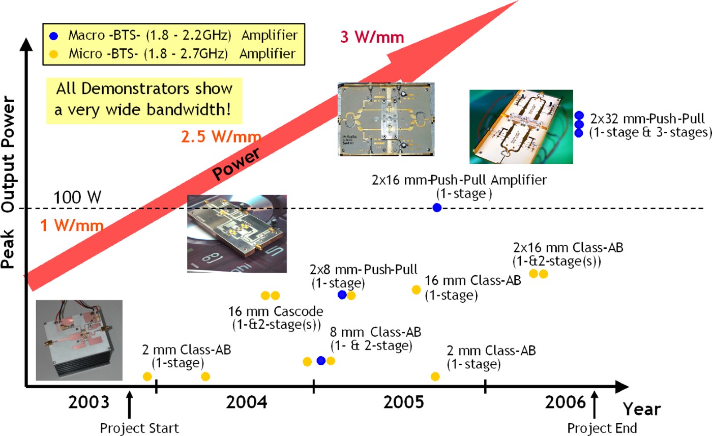
In retrospect, an impressive progress for AlGaN/GaN-based multiband PAs has been achieved by the close Alcatel-Lucent/FhG-IAF collaboration within the GANGLION project. Starting with a low power 34 dBm (peak) amplifier, the peak output power has been boosted up to 51.9 dBm – which means by 18 dB! In parallel, all demonstrators exhibited a large bandwidth and have been characterized successfully against 3GPP ACLR specification using a single-carrier W-CDMA signal, partially also using linearization and reduction of signal dynamic. Figure 8 gives a summarized overview on all GaN multiband amplifiers realized within GANGLION. It can be noticed that more than 15 amplifier demos have been commonly realized by Alcatel-Lucent and FhG-IAF within the three years project duration.

Fig. 8. Overview on GaN multiband amplifiers realized in GANGLION.
III. ELBA PROJECT – EFFICIENCY IMPROVED GaN-BASED PAs
While the main focus in GANGLION was a general investigation of the suitability of GaN technology for mobile radio multiband PA realization up to high output power levels, the main target in ELBA was to investigate promising amplifier concepts for efficiency improvement based on GaN technology. In order to achieve this, demonstrators for single- and multiband amplifiers have been realized and characterized using W-CDMA test signals in combination with reduction of signal dynamic and digital predistortion.
For this purpose, a single-band class-AB GaN amplifier was realized in the beginning in order to determine the current GaN technology status and limits of conventional class-AB amplifiers at the beginning of the project.
A) Single-band class-AB GaN amplifier
Figure 9 shows a photo of the realized 2.7 GHz class-AB amplifier, based on a W G = 32 mm GaN power cell. As shown by Fig. 10 the amplifier yielded up to approximately 49 dBm saturated output power at V DS = 34 V, when using a single-carrier W-CDMA signal. The estimated ACLR limit for linearizability of this technology is at about −33 dBc resulting in about 43 dBm average output power with a drain efficiency of 31%. The maximum gain after amplifier tuning is 13 dB.

Fig. 9. Photo of 2.7 GHz class-AB amplifier.

Fig. 10. Measured characteristic of single-band class-AB amplifier.
When using digital predistortion and at a supply voltage of V DS = 30 V, the spectrum of the single-carrier W-CDMA meets the 3GPP ACLR specification (−45 dBc at 5 MHz offset and −50 dBc at 10 MHz offset) up to an average output power of 42.3 dBm and 32.3% drain efficiency, as illustrated by Fig. 11.

Fig. 11. Measured single-carrier W-CDMA spectrum without and with linearization.
B) Single-band symmetrical GaN Doherty amplifier
In order to improve single-band efficiency, the symmetrical Doherty concept was chosen and a GaN-based Doherty amplifier for 2.7 GHz was designed based on a large signal model from FhG-IAF and subsequently realized. Figure 12 shows a photo of this amplifier demonstrator, which is based on two W G = 32 mm power cells. Feeding the signal to the main amplifier and the auxiliary amplifier, a 90°, 3 dB hybrid is used on the input side. In order to increase the bandwidth of the output transformator, a shorted quarter-wave stub has been added.

Fig. 12. Photo of a symmetrical Doherty amplifier.
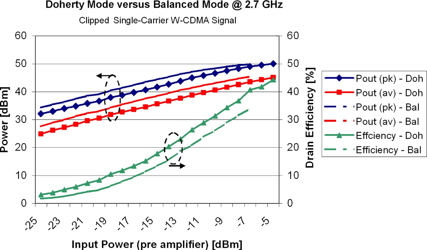
After manually tuning of the output matching network i.o. to ensure a proper load modulation, the Doherty amplifier yielded a clear efficiency improvement at 2.7 GHz when compared to the previously presented class-AB amplifier as well as compared to when operating the Doherty in balanced mode. In both cases, a drain efficiency improvement of about 10% has been found. A measured performance comparison between balanced and Doherty mode is given by Fig. 13. The gain of the Doherty is about 9 dB.

Fig. 13. Measured characteristic in Doherty mode versus balanced mode.
Figure 14 shows the measured single-carrier W-CDMA spectrum in Doherty mode, when applying digital predistortion. Meeting 3GPP ACLR specification, the Doherty amplifier achieved up to 44.9 dBm average output power and 45% drain efficiency for V DS = 30 V.

Fig. 14. Measured single-carrier W-CDMA spectrum using digital predistortion.
In order to investigate multiband PA performance, a class-AB-based demonstrator, covering a frequency range from 1.8 to 2.7 GHz was designed using a packaged W G = 32 mm power cell. A photo of this multiband amplifier is shown in Fig. 15. In the same manner as the previously discussed devices, also this amplifier was characterized using a single-carrier W-CDMA signal with reduced signal dynamic and digital predistortion. Figure 16 shows the measured small signal characteristic of S11 and S21 as well as the linearized single-carrier output spectrum at the three different frequencies 1.8, 2.14 and 2.7 GHz. Up to 2.5 GHz, the multiband amplifier showed very good drain efficiencies of >30%, meeting 3GPP ACLR requirements. The associated average output power is around 40 dBm. At 2.7 GHz the amplifier showed a decrease by ∼5% in drain efficiency and 2.5 dBm in output power, while the gain is relatively constant at about 12 dB across the whole frequency range.

Fig. 15. Photo of highly efficient class-AB multiband amplifier.

Fig. 16. Measured characteristic of class-AB multiband amplifier.
C) Envelope tracking (ET) for efficiency improved single- and multiband GaN amplifier
The previously discussed Doherty concept constitutes a good solution to improve single-band PA efficiency at reasonable circuit complexity, but e.g. due to frequency-dependent load modulation and quarter-wave sections, the basic concept is not really suited for efficiency improved multiband amplifier applications.
In contrast to this, the ET concept based on a class-AB RF amplifier is a very promising concept in order to improve efficiency of single- as well as of multiband amplifiers. This is possible due to the fact that the ET modulator is independent from the carrier frequency and a class-AB amplifier can be designed for multiband operation, as shown by the previously described multiband solution. In the following, the ET concept is described in more detail.
The efficiency of linear PAs can be increased by dynamically varying the bias point, thereby reducing the quiescent power dissipation of a PA when the output power decreases. Linear PAs with dynamic supplies have been investigated by means of a bias control applied to the drain terminal of aGaN-based HEMT.
The RF PA is biased in class-AB mode in order to trade-off linearity and efficiency. With dynamic control of the drain bias voltage, the quiescent point moves horizontally for a fixed drain current (Fig. 17).

Fig. 17. Drain modulation principle.
The area below Ids1 and Qfix exemplarily represents the consumed DC power if the PA is supplied with a maximum fix supply voltage. Vlow is the lower supply voltage limit for the RF amplifier. When applying ET, the supply voltage Vet is modulated between Vlow and Vmax. The consumed DC power for ET operation is thus represented by the area below Ids1 and Qet. Depending on the RF signal, Qet is moving and the consumed power under ET operation is thus changing depending on the RF signal. The power saving for ET is finally represented by the area below Qet and Qfix and can be significant for signals with high PAR.
Figure 18 shows the efficiency of class-A and class-B amplifiers. Both amplifiers are reaching good efficiency figures at full output power, but they are decreasing when using high PAR signals like those used in modern communication schemes.

Fig. 18. Efficiency curves of class-A and-B operation.
In order to gain efficiency within the ET architecture, the drain voltage should follow as accurate as possible the envelope signal, so that the RF PA is always operated close to its saturation point. In order to guarantee good overall ET performance, the envelope modulator has to amplify linearly and efficiently the envelope signal.
In the ideal case (theoretically 78% efficiency), a class-B biased RF PA combined with a accurate envelope modulator featuring 90% efficiency could optimally reach 70% overall drain efficiency. In a real application, overall efficiency figures of 50% are more realistic considering a class-B RF amplifier with 60% efficiency and an envelope modulator with 80% efficiency [Reference Kimball6].
The block diagram shown in Fig. 19 describes an ET system featuring an envelope amplifier which adjusts the supply voltage (i.e. the drain voltage) of the class-AB stage dynamically by following the signal envelope.

Fig. 19. Block diagram of the ET system for 3-/4-G radio transmitters.
By following the envelope which represents the magnitude of the I&Q – signal vector, the peak load efficiency of the system is improved. However the requirement for high bandwidth high power and linearity to the envelope modulator results in lower overall efficiency at different loads. It is worth noticing the mandatory need to delay the RF input signal in order to synchronize both envelope path and the RF path. Such time mismatch as well as voltage ripple at the DC-feed of the output stage would degrade efficiency and linearity of the ET architecture.
The total efficiency can be calculated by means of the general equation for dynamic biasing schemes [Reference Ertl, Kolar and Zach1].
It is evident that the whole stage efficiency is strongly depending on the efficiency of both the envelope modulator and the RF PA.
The envelope modulator has been realized using a common circuit topology which has been inspired from the audio domain and is called switch mode assisted linear amplifier [Reference Ertl, Kolar and Zach1]. The DC-coupled envelope amplifier comprises a wide bandwidth class-AB linear stage to provide a wideband voltage source by linearly following the envelope signal and, in parallel, a switching stage to provide an efficient current supply (see Fig. 20). The current is supplied to the drain of the RF amplifier from both the switching stage and the linear stage controlled by the current sensor which senses the error current flowing out of the linear stage and turns on/off the efficient power switch.

Fig. 20. Block diagram of the in Bell Labs realized ET modulator.
The closed-loop linear stage provides the difference between the desired output current and the current provided by the switched MOSFET stage, such that the overall error is minimized.
Following this concept an ET system setup based on GaN-HEMT devices from FhG-IAF Freiburg has been built at Bell Labs Germany. A photo of an exemplarily ET modulator combined with an RF PA as well as a measured single-carrier output spectrum measured with the ET system is shown in Figs 21 and 22, respectively.

Fig. 21. Photo of an exemplarily ET modulator and PA.

Fig. 22. Exemplariliy measured single-carrier W-CDMA spectrum.
IV. SUMMARY
Summarizing six years of GaN technology development and GaN-based PA design AlGaN/GaN-based RF power HEMTs turned out to be the enabling technology for realization of highly efficient single- as well as multiband RF PAs. Within GANGLION and ELBA project, various RF PA demonstrators have been designed and realized addressing single- and multiband applications. Peak output power levels up to 51.9 dBm achieved with a GaN-based multiband amplifier as well as high drain efficiency up to 45% using a single-carrier W-CDMA signal in combination with clipping and digital predistortion based on a symmetrical Doherty are some highlights of the projects indicating the potential of GaN technology. Finally, the current work at Bell Labs on ET based on GaN technology, has been described, targeting at future highly efficient multiband PAs.
ACKNOWLEDGEMENT
The authors acknowledge the support of the Germany Ministry of Education and Research (BMBF) under contract 01BU382 and 01BU600 in the context of ‘mobileGaN’ and ‘mobileInternet’, respectively. The continuous support by the epitaxial and technology department at Fraunhofer IAF and of the Alcatel-Lucent model shop is gratefully acknowledged.
 Dirk Wiegner is a member of technical staff in the Bell Labs' Narrow/Broadband RF Transceivers/Amplifiers Department of the Wireless Access Research Domain in Stuttgart, Germany. He received the Dipl.-Ing. degree in electrical engineering in 2001 at the University of Stuttgart, Germany. At Alcatel-Lucent, he first was engaged in characterization and modelling of SiGe and BiCMOS devices as well as in investigation of AlGaN/GaN HEMT technology for multiband power amplifiers within the microelectronics research department. In 2006 he changed to the Narrow/Broadband RF Transceivers/Amplifiers Department where he is currently working on base stations for mobile telecommunication focusing on high efficient power amplifier concepts and technologies as well as on multiband and multi-standard capable amplifier solutions.
 Gerhard Luz received his Dipl.-Phys. from the University of Stuttgart, Germany in 1979. He joined the research center of the former Standard Elektrik Lorenz AG and worked at InP optoeletronic device characterization. In 1986 he changed to packaging of optoelectronic devices. From 1996 he was responsible for fiber coupling and packaging of passive optical devices in Alcatel R&I. In 2003 he changed to the radio department and works currently mainly on power amplifier development. He is present member of technical staff in the Bell Labs Department at Alcatel-Lucent.
 Robin Machinal received the B.S. degrees from the Université of Bordeaux, France in 2002 and the M.S. degree from the University of Strasbourg, France from the department of micro- and nano-electronics in 2006. Since October 2006 until present, he has been investigating new RF power amplifier architectures for next generation of radio transmitter based on the envelope tracking system. His research interests at Bell Labs, Germany, include dc–dc switching converters, topologies and controls for high switching frequency, high efficiency converters, hybrid linear amplifiers, high power and high speed electronics as well as GaN technology.
 Patrick Jüschke received the Dipl.-Ing. degree in information technology from University of Cooperative Education of Stuttgart, Germany in 2008. He is working for Alcatel-Lucent Bell-Labs Stuttgart in department of RF transceivers and amplifiers since January 2008. He is currently working on amplifiers and PA concepts for complex modulated signals like UMTS, OFDM, etc. with focus on envelope tracking and future amplifier concepts.
 Andreas Pascht is leading the Bell Labs Department Narrow/Broadband RF Transceivers/Amplifiers of the Wireless Access Research Domain in Stuttgart, Germany. The department is dealing with signal conditioning issues, transceiver architectures, and power amplification concepts for narrowband and broadband transceiver solutions.
He received the Dipl.-Ing. and the Ph.D. degree in electrical engineering in 1996 and 2001 at the University of Stuttgart, Germany.
At Alcatel-Lucent he was first leading a transceiver team in the wireless area. After that he led the technical part of the internal venture for software-defined radio. After transferring the results into the Business Group he was a Unit Manager for transceiver topics within the wireless research organization. Andreas Pascht is a member of the Alcatel Technical Academy.
 Wolfgang Templ graduated in Physics from University of Stuttgart in 1987. He received his Ph.D. from Max Planck Institute for Metal Physics/Stuttgart in 1990 on the field of muon spin rotation-based investigations of spin density waves in antiferromagnetic Chromium. After two years postdoc at MPI working on nuclear methods in solid state physics at Paul Scherrer Institute (Switzerland) and Rutherford Appleton Labs (UK) he joined Alcatel-SEL in 1992 where he worked for four years in the field of semiconductor component qualification and tests. From 1999 to 2005 Wolfgang Templ lead the microelectronic technology group of Alcatel Research Centre. Today he is mainly concentrating on identification, assessment, and introduction of new device technologies for optical and wireless communication systems. Wolfgang Templ is a member of the Alcatel-Lucent Technical Academy.
 Ulrich Seyfried, born 1953 in Michelstadt/Odenwald, received his diploma in Physical Techniques at FH Wiesbaden in 1977. After military services he joined SEL in 1978, where he first worked in applications for electrical switches. In 1979 he changed to the Corporate Research Centre, working on applications for piezo ceramics and development of fiber optics for 13 years. From 1992 to 2003 he worked on parameter extraction and modeling of semiconductor devices. In 2004 he joined RF-amplifier research team focusing on characterization of GaN-based circuits.
 Thomas Merk received his Dipl.-Ing. (B.A.) from the University of Cooperative Education Stuttgart in 2004. After his diploma thesis on broadband GaN power amplifiers at Alcatel R&I he changed to the mobile radio development department where he is responsible for the design and simulation of power amplifiers. Currently, he is focusing on amplifier designs for multicarrier GSM and LTE. Furthermore, his interests include all kinds of RF and 3D electromagnetic simulation techniques.
 Rüdiger Quay received the Diplom degree in physics from Rheinisch-Westfälische Technische Hochschule (RWTH), Aachen, Germany, in 1997, and a second Diplom in economics in 2003. He received his doctoral degree in technical sciences (with honors) from the Technische Universität Wien, Vienna, Austria. In 2009 he received the venia legendi (habilitation) in microelectronics, again from the Technische Universität Wien. He is currently a research engineer with the Fraunhofer Institute of Applied Solid-State Physics, Freiburg, Germany, heading the RF-devices and characterization group. He has authored and coauthored over 100 refereed publications and three monographs. He is a member of IEEE, MTT, and chairman of MTT-6.
 Friedbert van Raay was born in Hilden, Germany, in 1960. He received a M.Sc. degree in electrical engineering from Technical University of Aachen, Germany, in 1984, and a Ph.D. degree from the University of Kassel in 1990. From 1992 to 1995, he was with the SICAN GmbH, Hannover, Germany, working on RF system development and measurement techniques. In 1995, he returned to the University of Kassel as a senior engineer. He supervised the Microwave Group within the Institute of High Frequency Engineering and worked on design of ultra-broadband GaAs MMICs, device modeling, and large-signal measurement techniques. In November 2001, he joined the Fraunhofer Institute of Applied Solid-State Physics in Freiburg, Germany. His research interests include MMIC design, device modeling, and measurement techniques.