


I. INTRODUCTION
AlGaN/GaN high electron mobility transistors (HEMTs) on various substrates have raised a lot of interest for the application in future high-efficiency base station systems for next generation mobile communication, currently dominated by laterally diffused metal oxide semiconductor technology. Using GaN technology in a transmitter, infrastructure equipment manufacturers will benefit from major improvements in system performance and flexibility. A second, very attractive application of GaN HEMTs is high-power, high-efficiency, and broadband GaN MMIC between 6 and 18 GHz and beyond. Besides performance it will be crucial to match or even exceed the device reliability of other technologies in order to be competitive. Due to its wide band gap, high breakdown field, current density, and saturated velocity, this material system is well suited for high-temperature and high-power applications from RF to millimeter wave frequencies. Much progress has been made in improving device performance to the extent that researchers have reported record numbers for channel charge density and power density exceeding 2 × 1013 cm−2 and 30 W/mm at 4 GHz [Reference Wu1].
However, several difficulties such as high-voltage operation stability [Reference Dora, Chakraborty, Mccarthy, Keller, Denbaars and Mishra2], carrier trapping [Reference Green, Tilak, Kaper, Smart, Shealy and Eastman3], and reliability [Reference Nikaido, Kikkawa, Yokokawa and Tateno4, Reference Kikkawa, Imanishi, Hara, Shigematsu and Joshin5] have to be overcome in order to realize the performance requirements and to fabricate devices that may be used commercially. Here, we present results from our 3- and 4-in. GaN HEMT technology demonstrating very promising performance and reliability data.
II. EPITAXIAL GROWTH
Incoming 4H-SiC(0001) substrate wafers are first classified using polarized light imaging in order to examine the defect distribution (see Fig. 1). Substrates having a high defect density are utilized for calibration growths whereas substrates having a low defect density are used for subsequent device processing.

Fig. 1. Inspection results from polarized light imaging of 3-in. SiC(0001) substrates showing a low defect density wafer (top) and a wafer having a high defect density (bottom).
Epitaxial growth of the AlGaN/GaN heterostructures is carried out by either metal organic chemical vapor deposition (MOCVD) or molecular beam epitaxy (MBE). In the case of MOCVD growth is performed in an Aixtron 12 × 3-in. multiwafer reactor using trimethylgallium, trimethylaluminium, and ammonia as precursors in hydrogen carrier gas. In our Veeco GEN20A MBE system wafer diameters up to 4-in. are used. Elemental sources for Ga and Al are utilized and active nitrogen is generated from N2 via an RF plasma cell. Compared to typical MOCVD growth temperatures of 1100 °C the deposition temperature in MBE is about 350–400 °C lower. In both cases it is important to provide an insulating buffer which can either be realized by suitable growth conditions (see e.g. [Reference Poblenz6]), and by Fe and C doping for MOCVD [Reference Heikman, Keller, Den Baars and Mishra7] and MBE [Reference Poblenz, Waltereit, Rajan, Heikman, Mishra and Speck8], respectively.
In both cases epitaxial growth starts with an AlN nucleation layer followed by a GaN buffer layer and the AlGaN barrier. The structures are capped with a thin GaN layer [Reference Waltereit9]. Both the composition and the thickness of the active region are calibrated by high-resolution X-ray diffraction in conjunction with dynamic simulation of the profiles (see e.g. [10]). In order to achieve smooth surfaces free of metallic Ga, we employ Ga-rich deposition conditions for MBE with periodic growth interruptions in order to desorb excess Ga from the surface [Reference Poblenz, Waltereit and Speck11]. Both MBE and MOCVD yield atomically flat interfaces and surfaces with excellent homogeneity in AlGaN composition and thickness (see Fig. 2). Such a homogeneity is required in order to achieve low standard deviations in threshold voltage across an entire 3-in. wafer well below 100 meV with sheet resistance standard deviations below 1% (see Fig. 4). The sheet carrier concentration n sheet as determined by Hall effect measurements after growth is dominated by the large spontaneous and piezoelectric polarization fields in the AlGaN/GaN materials system [Reference Bernadini, Fiorentini and Vanderbilt12]. As seen from Fig. 3, n sheet of MOCVD and MBE grown samples increases with Al-content in the barrier as expected from the increase in fixed polarization charge at the AlGaN/GaN interface. Interestingly, we find consistently lower values in n sheet for MBE grown samples compared to their MOCVD counterparts. Since the in-plane lattice constants a of the GaN buffer layers of MBE and MOCVD material are identical within the resolution of our X-ray equipment (Δa/a ~ 4 × 10⁻⁵ obtained from the measured Δc/c), we conclude that also the strain states of the AlGaN barriers are identical. Therefore, we suspect that the surface potential of MBE grown samples differs from that of MOCVD grown samples. Photoreflectance measurements of representative samples from this series return a surface potential around 0.6 and 0.3 eV for MBE and MOCVD grown samples, respectively. This difference is removed by device processing utilizing a SiN surface passivation and a Schottky gate metallization [Reference Köhler13].

Fig. 2. High-resolution X-ray diffraction profiles across the GaN(0002) reflection of a AlGaN/GaN heterostructure grown on a 4-in. SiC(0001) substrate by MBE. Note the excellent homogeneity as evidenced by the agreement of the profiles measured along a line at different distances R from the wafer center.

Fig. 3. Sheet carrier concentration of AlxGa1–xN/GaN HEMT structures grown by MOCVD (squares) and MBE (circles) on s.i. SiC substrates as a function of the Al-content in the barrier layer. Note the difference in sheet carrier concentration between MOCVD and MBE.
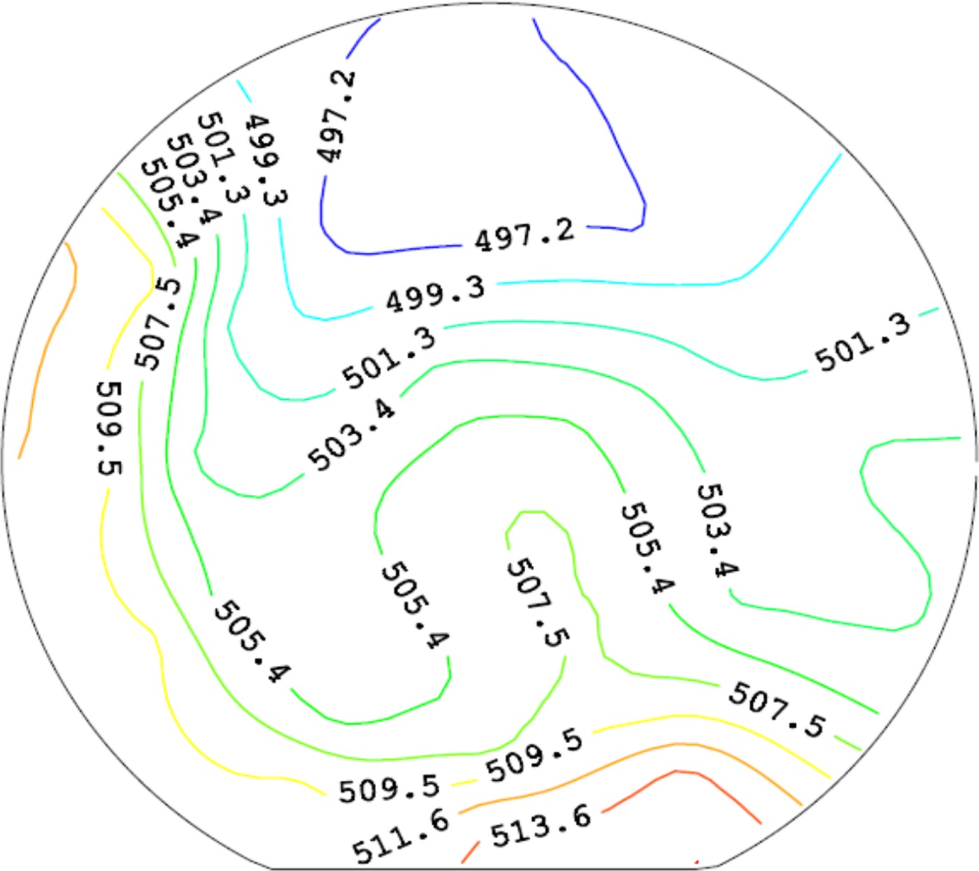
Fig. 4. Sheet resistance (Ω/sq) map of a 3-in. AlGaN/GaN HEMT wafer as determined by a contactless measurement after MOCVD growth.
For MOCVD a 22 nm Al0.22Ga0.78N barrier and a 3 nm thin GaN cap typically leads to sheet carrier concentrations and mobilities of 8 × 1012 cm−2 and 1500 cm2/V s, respectively, yielding sheet resistances around 500 Ω/sq (Fig. 4). These values are reproducibly obtained with uniformities better than 2% across the entire wafer. The threading dislocation density is in the low 108 cm−2 range as determined by plan-view transmission electron microscopy, the surface roughness as studied by atomic force microscopy is well below 0.5 nm over an area of 10 × 10 µm2, and the buffer isolation resistance at 60 V is well above 1012 Ω/sq for a 4 µm gap test structure.
For MBE we typically observe very similar data except for mobility and threading dislocation density in agreement with state of the art MBE material from other groups (see e.g. [Reference Waltereit, Poblenz, Rajan, Wu, Mishra and Speck14]). The mobility in MBE grown samples is about 10–20% lower than in MOCVD grown samples, whereas the density of threading dislocations in MBE material is about 1010 cm−2.
III. PROCESSING
Processing technology is based on standard III–V processing equipment and is divided into frontside and backside processing. Frontside processing involves implantation isolation, alloyed Ti/Al/Ni/Au ohmic contacts, Ni/Au gates, SiN passivation, Au-based interconnect metals, and electroplated Au airbridges. The gate length is 0.5 µm for 1–6 GHz applications, 0.25 µm for devices between 6 and 18 GHz, and 0.15 µm for frequencies above 20 GHz. All frontside lithography steps are carried out on an optical stepper except for sub 0.5 µm structures that are defined using electron-beam lithography.
Ohmic contacts are optimized for both low contact resistance and smooth morphology for improved marker recognition. Gates are processed with integrated field plates and source terminated shields in order to reduce the electric fields at the gate region. Integrated circuits furthermore involve thin film resistors, high-voltage capacitors, and inductors for impedance matching to a 50 Ω environment [Reference Benkhelifa15, Reference Schuh16]. Capacitors have a breakdown voltage well beyond 200 V. After frontside processing, the wafers are mechanically thinned to 100 µm for backside processing where device definition is carried out using contact mask alignment to the frontside. Front-to-back viaholes are etched through the thinned substrate and the epilayer. The backside is metallized and electrically connected through the viaholes to the source contacts on the frontside (Fig. 5).

Fig. 5. Cross-section of a metallized front to back source contact via after focused ion beam preparation. Note the excellent coverage of the via.
In the following we briefly summarize key improvements in processing in order to obtain high performance and reliable devices. An important prerequisite for low source and drain resistances is an ohmic contact with low contact resistance. We employ a Ti/Al/Ni/Au-based contact metal that is annealed by rapid thermal annealing (RTA) for 30 s in nitrogen atmosphere. Optimization of the annealing temperature is crucial as too low temperatures do not yield a true ohmic behavior of the contact and too high temperatures may lead to a morphological degradation of the contact causing potential gate–source or gate–drain breakdown. The results of the optimization are shown in Fig. 6. Using an annealing temperature of 825°C we achieve a contact resistance around 0.2 Ω mm while still maintaining an edge definition better than 100 nm (not shown here).

Fig. 6. Optimization of the ohmic contact annealing process: dependence of the ohmic contact resistance as a function of RTA temperature.
Next to low access resistance it is important to suppress parasitic gate and drain currents. In Fig. 7 the impact of two different gate processes on gate and drain leakage is shown. For each variant (labeled “A” and “B”) four wafers were processed within the same batch. The improvement in leakage at 50 V drain bias is about two orders of magnitudes and is mainly achieved by improvements in the gate and the passivation modules. The impact of the processing variant on other DC or RF parameters is, if any, marginally.

Fig. 7. Dependence of the leakage current density at 50 V drain bias (gate bias −7 V) on two different gate processes “A” and “B”.
Processed wafers are examined using DC mapping, high-voltage breakdown tests, pulsed current–voltage (IV) characterization, load-pull measurements as well as DC and RF reliability tests.
IV. HEMT PERFORMANCE
In this section we discuss results from our 250, 500, and sub 250 nm gate length technologies. All devices will be shown to have both high power added efficiency (PAE) and low leakage currents, thus demonstrating that we have successfully achieved high isolation and low trap densities in our devices. The small gate periphery results are representative for both growth methods, i.e. we do not see specific differences between MBE and MOCVD.
We begin with the 250 nm gates. Continuous-wave load-pull mapping of a structure with 1 mm gate periphery without intentional harmonic matching across all 21 cells on an entire 3-in. wafer (Fig. 8) yields a PAE of (50 ± 2)% per single wafer with only 2% scatter of the mean PAE from wafer to wafer (see Fig. 8). The same set of wafers also exhibits very low parasitic currents at high voltage with gate and drain leakage below 100 µA/mm at a drain bias as high as 150 V under pinch-off condition (Fig. 9).

Fig. 8. Load-pull mapping (continuous wave) results at 10 GHz and 30 V of 0.25 µm gate length HEMTs with 1 mm gate periphery across all 21 cells of an entire 3-in. wafer: (top) Overlay of the power sweeps and (bottom) PAE (blue), output power (red) and gain (green) of a batch of six wafers. Note the excellent homogeneity and reproducibility.

Fig. 9. Leakage currents (mA/mm) of a 250 nm gate length process control monitor structure at a drain bias of 150 V and a gate bias of −7 V.
Next, we investigate 500 nm gates. Load-pull power measurements (2 GHz) are carried out on devices having a gate width of 800 µm. Figure 10 shows an overlay of power sweeps of all 21 cells of a single wafer taken at a drain bias of 50 V in class A/B. Identical tuning was utilized for all cells in order to assess both performance and homogeneity. The maximum PAE is around 60%, the power density is 10 W/mm, and the linear gain around 23 dB. The homogeneity of the power data is excellent with standard deviations well below 3% for power, PAE, and gain. Furthermore, very good reproducibility from wafer to wafer is observed with the mean PAE, gain and output power being within 2% for several wafers processed sequentially (see Fig. 10).

Fig. 10. Load-pull mapping at 2 GHz and 50 V of 0.5 µm gate length HEMTs with 800 µm gate periphery across all 21 cells of an entire 3-in. wafer. Note the excellent homogeneity (top) and reproducibility (bottom).
In Fig. 11 the dependence of the continuous-wave power density, linear gain, and PAE on drain bias up to 100 V is plotted. The output power density scales linearly with drain bias showing the absence of knee walkout or pinch-off problems at large drain bias. A power density of 26 W/mm is reached at 100 V. The PAE is beyond 60% for all bias values with its peak value close to 70% for a drain bias around 60 V. As expected, the gain increases with bias voltage.

Fig. 11. Load-pull measurements (2 GHz) of 0.5 µm gate length HEMTs (800 µm gate width) versus drain bias. Note that the PAE remains above 60% up to 100 V.
As a result of the homogeneous and reproducible technology large periphery devices (36 mm gate width) were diced from the wafers and packaged in industry-standard ceramic packages [Reference Waltereit17]. On these devices an output power beyond 125 W is achieved with a PAE above 60% and a linear gain around 16 dB as demonstrated in Fig. 12.

Fig. 12. Power sweep (continuous wave) of a packaged 36 mm gate width power bar at a frequency of 2.14 GHz and a drain bias of 50 V. The transistor is biased in class AB.
Last the GaN HEMT technology is described based on both 150 and 100 nm gate lengths defined by electron-beam lithography. Devices both with and without field-plates optimized to mm-wave operation are used. Field-plated short-gate-length GaN HEMTs are developed for superior large-signal performance at millimeter-wave frequencies and increased reliability while the additional capacitances of the field-plates have to be optimized with respect to high-speed operation. GaN with a gate-width between 0.1 and 0.48 mm yield a maximum drain current of >0.9 A/mm and a maximum transconductance g m of more than 400 mS/mm without a gate recess, measured at V DS = 7 V. With the application of a gate recess, the maximum transconductance can be increased to above 550 mS/mm for the same voltage and gate length. The current gain cut-off frequency f T of the GaN HEMT is beyond 50 GHz at V DS = 7 V for a gate length of 150 nm without a gate recess. This also can be increased beyond 80 GHz with the application of the gate recess. The maximum frequency of oscillation at V DS = 7 V can be as high as f MAX > 200 GHz for the 100 nm gate technology. Currently the maximum operation voltage is V DS = 25–30 V for a gate length of 150 nm with a corresponding on-state breakdown voltage of BV DS > 65 V. For devices with 100 nm gate length, this maximum operation bias reduces to 15–20 V. CW-load-pull measurements for a GaN device with a gate width of Wg = 0.48 mm yield a saturated output power density of >4 W/mm at 27–30 GHz, a linear gain of 5–7 dB when tuned for maximum output power. Power-added efficiency reaches 30% in CW and more than 45% in pulsed operation at 27 GHz.
V. RELIABILITY
DC and RF reliability tests are undertaken at 50 and 30 V drain bias in order to assess the long-term stability of the devices having a gate length of 500 and 250 nm, respectively. The tests are carried out without any burn-in procedure. The channel temperatures given here are calibrated using the thermal resistance determined by Raman thermography [Reference Kuball18]. Here we present the status for initial tests on MOCVD material.
The packaged HEMT devices for DC tests have a gate width of 480 µm. DC assessment is performed with a fixed gate bias to obtain an initial drain current density of 50 mA/mm for 500 nm gates and 150 mA/mm for 250 nm gates. In Fig. 13 the relative change in drain current and the absolute gate current versus time is shown for 250 nm gates (top) and 500 nm gates (bottom). Below 10% drain-current change is observed after more than 1000 h of operation. Throughout the tests the gate currents remain well below 1 mA/mm even for channel temperatures as high as 260 °C for the 250 nm gate technology. These results furthermore underline the excellent optimization of epitaxial growth and processing for reliability. The extrapolated DC lifetime for the 500 nm gate length technology is around 20 years for a degradation criterion of 20% drain current change [Reference Waltereit19].

Fig. 13. Drain current change and absolute gate currents in DC reliability tests of 250 nm gates (top) and 500 nm gates (bottom). The drain current at the beginning of the test is 50 mA/mm for 500 nm gates and 150 mA/mm for 250 nm gates.
RF tests are performed at 2 and 10 GHz operating frequency under 1 dB compression for a gate length of 500 and 250 nm, respectively. The test vehicle for the 2 GHz tests is a multifinger FET with a total gate width of 2.4 mm whereas the 10 GHz tests are performed on a single stage MMIC with a gate width of 1 mm. In Fig. 14 we show the change in gain for both gate length technologies. The change in gain is well below 0.5 dB during the first 1000 h of the test indicating also a promising RF reliability. It should be noted that gate and drain current during testing remain very stable.

Fig. 14. RF reliability of 250 nm gate technology (top) at 30 V drain bias on a single stage MMIC and of the 500 nm gate technology (bottom) at 50 V drain bias on a multifinger FET.
VI. SUMMARY AND CONCLUSION
High-quality AlGaN/GaN HEMTs have been fabricated uniformly and reproducibly on 3- and 4-in. SiC substrates. The devices exhibit excellent high-voltage stability with parasitic gate and drain currents well below 1 mA/mm at 150 V even for 250 nm gates. Excellent large signal properties with PAE values at 2 GHz exceeding 60% up to 100 V drain bias were presented. As a result of the homogeneity and reproducibility power bars with 32 mm gate width have been fabricated. These power bars deliver more than 125 W output power at a frequency of 2 GHz with a PAE above 60% and gain around 15 dB. Similarly, at 10 GHz we achieve very good performance with a PAE around 50% using 250 nm gate length technology devices. It should be stressed that these values achieved very homogeneously and reproducible.
It is demonstrated that an optimized approach in both epitaxy and processing does indeed lead to excellent device lifetimes at 30 V (250 nm gates) and 50 V drain bias (500 nm gates) under both DC and RF conditions. Under DC conditions the drain current changes by only 10% during the first 1000 h for testing at elevated temperatures with stable gate currents. Under RF conditions, stable operation is observed for the duration of the test (1000 h) with an output power change below 0.2 dB.
ACKNOWLEDGEMENTS
The authors acknowledge the continuing support of the Federal Ministry of Defense (BMVg), the support of the Federal Ministry of Education and Research (BMBF), the Federal Office of Defense Technology and Procurement (BWB), the Bundeswehr Technical Center for Information Technology and Electronics (WTD 81), the European Space Agency and NXP. Continuous collaboration with United Monolithic Semiconductors (UMS) is highly appreciated.
 Patrick Waltereit received the Diploma degree in Physics from the Free University Berlin, Germany, in 1998 and the Ph.D. degree in Physics from the Humboldt University Berlin, Germany, in 2001 where he grew and characterized non-polar oriented GaN/AlGaN heterostructures. He worked as a post-doctoral researcher at the University of California, Santa Barbara, CA, from 2001 until 2004 investigating molecular beam epitaxy for GaN-based electronic and optoelectronic devices. Currently, he is with the Fraunhofer Institute for applied solid state physics in Freiburg, Germany, where he is involved in project development and technology for GaN-based electronic devices. He has authored or co-authored over 70 technical publications and conference presentations.
 Wolfgang Bronner was born in Kandern, Germany, in 1956. He studied Physics at the Albert-Ludwigs-Universität in Freiburg where he earned his Diploma in 1984 and his PhD degree in 1989. In 1984 he joined the Fraunhofer Institut Solare Energiesysteme in Freiburg where he investigated the hetero epitaxy of GaAs on Si and on GaAs/SiO2 for solar cell applications. Since 1991 he is with the Fraunhofer Institut Angewandte Festkörperphysik (IAF) working on III–V technology. He is involved in the process development and fabrication technologies of various electronic and optoelectronic devices, such as GaN HEMTs and quantum cascade lasers. He mainly manages all plasma assisted processes at IAF.
 Rüdiger Quay received the Diplom degree in physics from Rheinisch-Westfälische Technische Hochschule (RWTH), Aachen, Germany, in 1997, and a second Diplom in economics in 2003. He received his doctoral degree in technical sciences (with honors) from the Technische Universität Wien, Vienna, Austria. In 2009 he received the venia legendi in microelectronics, again from the Technische Universität Wien. He is currently a research engineer with the Fraunhofer Institute of Applied Solid-State Physics, Freiburg, Germany, heading the RF-devices and characterization group. He has authored and coauthored over 100 refereed publications and three monographs. He is a member of IEEE, MTT, and chairman of MTT-6.
 Michael Dammann received his Diploma degree in physics from the Technical University in Karlsruhe, Germany in 1989 and his Ph.D. degree in technical sciences from the Swiss Federal Institute of Technology in Zurich, Switzerland in 1994. From 1994 to 1995 he worked at the Swiss Federal Laboratories for Materials Testing and Research in Dubendorf, Switzerland where he investigated the reliability of silicon pressure sensors. Since 1996, he has been with the Fraunhofer Institute of Applied Solid State Physics, Freiburg, Germany working on reliability and failure analysis of microelectronic and optoelectronic compound semiconductor devices.
 Rudolf Kiefer received his Dipl. Phys. degree in physics from the University of Freiburg, in 1979. He joined the Fraunhofer Institute of Applied Solid State Physics (IAF) in 1980 starting work on liquid crystal displays. For work on this topic he received a Ph.D. degree in physics in 1984 from the University of Freiburg. From 1984 to 1991 he investigated electro-optic effects in ferroelectric, liquid crystalline polymeric materials for optical storage applications. Afterwards he focused his work on studying a new switching effect of nematic liquid crystals to improve the viewing angle characteristics of thin film addressed liquid crystal displays (TFT-LCD). For this work he received a SID Award in 1998. In 1994 he moved to the field of III-V optoelectronic semiconductor technology. He managed different technology projects developing processes for fabrication and laser facet deposition of InP-based high-speed laser and GaAs as well as GaSb-based high-power laser. From 2000 his work is focused on the development of GaN semiconductor technology for MMICs.
 Wilfried Pletschen received his Dipl. Phys. degree in physics from the Technical University of Aachen, in 1981 with a thesis about Metal-Organic Molecular Beam Epitaxy. Afterwards he worked on Raman Spectroscopy of gases used in MOCVD systems and on semiconductors having a main focus on semiconductor surfaces. For work on the latter topic he received a Ph.D. degree in physics from the Technical University of Aachen in 1986. Since 1987 he is with the Fraunhofer Institute of Applied Solid State Physics (IAF) in Freiburg working in the field of semiconductor technology. He has developed processes for lasers, IR photodetectors, bipolar and field effect transistors based on a variety of III-V materials including nitrides. For his work on GaAs/GaInP heterobipolar transistors he received a Fraunhofer award in 1993. Since 2008 he is also involved in the technology of MEMS devices.
 Stefan Müller was born in Hanau, Germany, in 1967. He is currently supervising the MOCVD growth of AlGaN/GaN HEMT structures. He received his Diploma degree in physics in 1994 from Giessen University before joining Fraunhofer IAF in 1994. He is working on MOCVD growth and characterization of AlGaN/GaN HEMTs based electronic and optoelectronic structures for high-frequency and high-power applications. He is author or co-author of more than 20 peer-reviewed journal papers and various contributions to topical meetings.
 Rolf Aidam was born in Germany in 1970. He received his Diploma and Ph.D. degrees in Physics from the University in Karlsruhe, Germany in 1996 and 1998, respectively. His Ph.D. research focused on epitaxy of high-temperature superconductors for high-frequency applications. This work was done in cooperation with the Forschungszentrum of Karlsruhe, where he worked until 2000. From 2000 to 2002 he was with Robert Bosch GmbH developing electronics for automotive industries. In 2002 he joint the Fraunhofer Institute for Applied Solid-State Physics, IAF in Freiburg, Germany as a research physicist in the area of III-V molecular beam epitaxy. His research interests include InP and GaAs based electronics and optoelectronics as well as GaN based electronics.
 Hanspeter Menner was born in 1965. He received the Dipl. Ing. degree in communication engineering from Offenburg University of Applied Sciences, Germany, in 1995. Since 1996 he has been with the Fraunhofer-Institut für Angewandte Festkörperphysik in Freiburg (IAF), Germany. He is working on the molecular beam epitaxy as well as on the metal-organic vapor phase epitaxy of III-V semiconductor heterostructures.
 Lutz Kirste was born in Bonn, Germany, in 1971. He received his Dipl.-Min. and Dr. degree with honors from the RWTH Aachen University and Albert-Ludwigs University Freiburg (Germany) in 1998 and 2003, respectively. Since 2001 he is a member of the research staff at the Fraunhofer Institute of Applied Solid State Physics. The focus of his research is the structural and chemical characterization of compound semiconductors by X-ray diffraction techniques and secondary ion mass spectrometry.
 Klaus Köhler was born in 1951. He studied Physics at the Technical University of Karlsruhe, Germany, and received the Diploma and Ph.D. degree in Physics in 1978 and 1981, respectively. From 1981 to 1982 he was with the IBM Research Laboratory, San Jose, CA (USA) investigating electrical discharges for dry-etch processes. From 1983 to 1986 he was with the Max-Planck-Institut für Festkörperforschung in Stuttgart, Germany, where he conducted optical investigations on III–V semiconductor heterostructures. Since 1987 he has been with the Fraunhofer-Institut für Angewandte Festkörperphysik (IAF) in Freiburg, Germany, working on the molecular beam epitaxy as well as on the metal-organic vapor phase epitaxy of III-V semiconductor heterostructures. Dr. Köhler is a member of the German Physical Society (DPG)
 Michael Mikulla received his diploma degree in electrical engineering from the Technical University of Braunschweig, Germany, in 1989 and a Ph.D. degree from the University of Ulm, Germany, in 1994. From 1994 he has been with Fraunhofer IAF in Freiburg, Germany, working on both high-power semiconductor lasers and GaN-based high-power transistors and MMICs. He has authored and has published over 100 conference/journal papers. From 2002 he is the head of the III/V-Technology department of the institute and is also in charge of the GaN RF Power Electronics business unit.
 Oliver Ambacher received his Dipl.-Phys. and Dr. degrees with honors from the Ludwig-Maximilians and Technical University Munich in 1989 and 1993, respectively, where he was involved in the deposition and characterization of amorphous silicon for solar cells. In 1992 he received a German Science Foundation Graduate Research Fellowship. In 1993, he joined the Walter Schottky Institute of the TU-Munich to investigate the epitaxial growth of group-III nitrides based heterostructures. Since 1995 the research of his group is focused on fabrication of GaN based devices like UV detectors, surface acoustic wave devices or microwave amplifiers as well as on the understanding of polarization induced effects in group-III nitride heterostructures and quantum wells. 1998/99, he spent one year at Cornell University, Ithaca, NY, as an Alexander von Humboldt fellow, where he was involved in the optimization of polarization induced AlGaN/GaN HEMTs for high-frequency and high-power applications. He became a Professor of Nanotechnology and head of the Institute for Solid State Electronics located at the Technical University of Ilmenau in 2002. In 2004 he was elected as head of the new Center of Micro- and Nanotechnologies. Since 2007 he is the head of the Fraunhofer Institute of Applied Solid State Physics and Professor for Compound Microsystems in Freiburg, Germany.


