I. INTRODUCTION
The loaded line approach is often used to design true-time-delay phase shifters based on microelectromechanical systems (MEMS) technology [Reference Rebeiz1–Reference Van Caekenberghe and Vaha-Heikkila3]. Usually, the MEMS component is either a switch or a varactor. Switch–based loaded lines [Reference Du, Bao and Zhao4] provide only a certain phase resolution, which is typically related to the number of MEMS or control bits, e.g., a 360° phase shifter with 5 control bits has a resolution of 11.25°. Varactor–based loaded lines are capable providing a continuously tunable phase shift [Reference Van Caekenberghe and Vaha-Heikkila3], depending on the bias voltage. The bias voltage can be set accurately by high–resolution digital–to–analog converters (DAC). MEMS varactors usually consist of an airbridge, which is deformed by applying a bias voltage and therefore the distance as well as the capacitance between the bridge and an underlying conductor is changed. As the deformation of an airbridge is controllable only over a small range, the tunability for simple designs is typically in the range of 20–30% [Reference Rebeiz1].
A less established way to build microwave phase shifters is the usage of a nematic liquid crystal (LC) as tunable dielectric material. Recent publications for applications in the frequency range from 20 to 100 GHz include transmission line–based approaches, tunable loaded lines as well as tunable filters. Transmission line–based phase shifters have been realized in different waveguide technologies: Completely [Reference Lim, Margerum and Lackner5] and partly [Reference Gaebler, Goelden, Manabe, Goebel, Mueller and Jakoby6] filled hollow waveguides, inverted microstrip lines [Reference Dolfi, Labeyrie, Joffre and Huignard7–Reference Mueller, Scheele, Weil, Wittek, Hock and Jakoby9] and finline [Reference Koeberle, Hoefle, Chen, Penirschke and Jakoby10]–based approaches. Periodically loaded lines with LC-based varactors have been realized in coplanar waveguide (CPW) [Reference Goelden, Gaebler, Goebel, Manabe, Mueller and Jakoby11] and slotline [Reference Karabey, Goelden, Gaebler, Strunck and Jakoby12] topology. For more compact phase shifters, the usage of tunable filters [Reference Moessinger, Fritzsch, Bildik and Jakoby13] or hybrid couplers with tunable loads [Reference Bulja, Mirshekar-Syahkal, Yazdanpanahi, James, Day and Fernandez14] have been investigated.
A novel varactor topology, where LC is used as a tunable dielectric layer underneath fixed MEMS bridges is proposed in this work. The varactors will be used to build a tunable loaded line phase shifter in an RF MEMS–compatible technology [Reference Fritzsch15] . In comparison with other technologies the LC layer in the varactors may be very thin, leading to fast response times. The loaded line allows realizing a quite compact design with relatively low losses and a good input matching over a large bandwidth. Compatibility with an MEMS fabrication process offers the possibility to integrate tunable LC components with MEMS switches into a single device. The hybrid device benefits from different advantages of these two parts, mainly the continuous tunability of the LC and high phase shift values introduced by discrete states of the MEMS switch. A possible topology for a full 360° reflection phase shifter is described in the last section of this work.
LC, mainly known from displays and other optical applications, consists of anisotropic molecules and appears in the nematic phase as a milky, high viscous liquid. The rod-shaped molecules tend to align themselves along the surface (Fig. 1), especially when it is covered with an alignment layer. Another way of aligning the molecules is by using an external electrical or magnetic field, as the molecules align along those field lines as well. Due to the anisotropy of the molecules, these effects can be employed to tune the effective permittivity of an LC layer continuously.

Fig. 1. Molecule alignment principle for an LC-filled parallel plate varactor.
The principle of tuning is sketched in Fig. 1 for a parallel plate capacitor. Without an applied bias voltage, the molecules align themselves parallel to the electrode surface. When a bias voltage is applied (Fig. 1(b)), the molecules start to align along the electrical field, which is perpendicular to the electrode surface. The orientation of the molecules is obtained by an equilibrium between the forces created by the surface anchoring as well as the electrical field and is determined by the elastic forces among the LC molecules. By increasing the bias voltage, the molecules align more and more along the electrical field, until they are perpendicular to the electrodes. Once the electric field is released, the molecules turn backto the state shown in Fig. 1(a), as they align themselves in parallel to the surface.
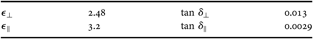
Permittivity values and the dielectric loss factors for the LC mixture used in this work are given in Table 1. The characterization has been carried out at 30 GHz, previous work with similar LC mixtures at 77 GHz [Reference Moessinger, Dieter, Menzel, Mueller and Jakoby16] has shown no significant change in permittivity values at higher frequency. The tolane matrix–based LC mixture [Reference Goelden, Lapanik, Gaebler, Mueller, Haase and Jakoby17] has been optimized for microwave applications; it has higher anisotropy and lower losses at microwave frequencies than a mixture for electro-optical applications.
Table 1. Properties of the used LC at 30 GHz and 23°C.
The appearance of the LC depends on the temperature, besides the nematic phase it may appear in two other phases: crystalline and isotropic. At low temperatures the material is present in the crystalline phase, the molecules are fixed in a lattice and therefore the orientation of the molecules is not adjustable. When the temperature rises above the melting point, the material enters the nematic phase, which allows the above–described tuning of the molecular alignment. By heating the LC further, above the clearing point, it enters the isotropic phase. In this phase, the molecules are randomly oriented; the LC appears as a transparent low–viscosity liquid.
Within the nematic phase, the electrical properties of the LC are temperature dependent. Figure 2 shows the permittivity as well as the loss tangent for a wide temperature range from 0 to 80 °C. The values have been measured using a cavity perturbation resonator [Reference Goelden, Lapanik, Gaebler, Mueller, Haase and Jakoby18] at 30 GHz, while the orientation of the molecules was controlled by an external magnetic field. Up to around 5 °C the LC is present in the crystalline phase, the material has no tunability. Above 5 °C the material is entering the nematic phase, the molecules may now be aligned and two different dielectric properties can be observed along their major axes. When the molecules are oriented perpendicular to the electric field component of the RF-field ɛ⊥ and tan δ⊥ can be measured. After rotating the external magnetic field by 90°, the molecules are aligned parallel to the electric field component of the RF-field and ɛ‖ as well as tan δ‖ can be measured. With increasing temperature two effects occur: The LC tunability τLC, defined as
is slightly decreasing, while the losses of the material are increasing. The clearing point of the used LC mixture is above 90 °C, the transition from nematic to isotropic phase lies outside the presented characterization region.

Fig. 2. Electrical properties of the used LC at 30 GHz.
II. DESIGN
A) Loaded line design
A loaded line consists of several unit cells, which are connected in series (Fig. 3). Each unit cell consists of a tunable shunt element connected to a part of non-tunable transmission line with a length of l/2 in front of and behind the shunt element. The input impedance of a periodic loaded line phase shifter can be approximated by the Bloch impedance Z b. For a loaded line with infinite length, the Bloch impedance Z b can be calculated according to [Reference Pozar19] by
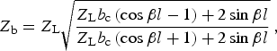
where b c is the susceptance of the shunt capacitance. To minimize reflections at the in- and output of the loaded line, the Bloch impedance should be equal to the reference impedance Z 0. According to (2), the impedance Z L of of the transmission line section on the loaded line must be higher than the Bloch impedance Z b. For a loaded line based on a CPW topology, the center conductor needs to become thinner and the gap wider compared to a normal CPW line of the same overall impedance.

Fig. 3. Schematic of a periodically loaded transmission line.
In order to achieve the maximum differential phase shift, low losses and good input matching, the parameters unit cell length, shunt capacitance, parasitic inductances and line impedance Z L need to be optimized according to the material tunability. A description of the optimization process can be found in [Reference Karabey, Goelden, Gaebler, Strunck and Jakoby12]. The presented loaded line was designed for a differential phase shift of 90° at 76 GHz with an input impedance of Z 0 = 50 Ω.
B) Unit cell layout
The single unit cell depicted in Fig. 4 consists of a CPW line on a 300 µm–thick fused silica substrate, where the ground planes are made of an approximately 5 µm–thick electroplated gold layer and the inner conductor is a 600 nm–thin multimetal layer. The varactor is formed by a 5 µm–thick gold bridge, which spans over the inner conductor and is later filled with LC. Due to the high line impedance of Z L≈120 Ω, the gap of the CPW line is relatively wide.

Fig. 4. Loaded line unit cell, (b) and (c) not to scale.
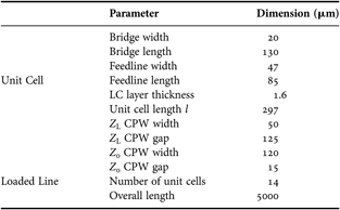
To reduce the parasitic inductance of the varactor, the bridge needs to be connected by broad feeding lines to the ground planes of the CPW line. The single varactors and unit cells have been designed within an optimization process by using a 2.5D EM solver [20]. The dimensions defining a unit cell are given in Table 2. The chosen thickness and dimension of the bridge implicate a high elastic spring constant. A small overlapping area with the metal underpass of 20 µm by 50 µm leads to a relatively low electrostatic force when the LC bias voltage is applied. Appreciable deformations of the bridge are therefore avoided.
Table 2. Unit cell and loaded line dimensions.
C) Test structure layout
In order to contact the loaded line with 50 Ω on-wafer probes, a short 50 Ω CPW line with a gold center conductor is placed at both sides of the loaded line, as can be seen in Fig. 5. Due to technological reasons, a via transition from gold to multimetal inner conductor is necessary.

Fig. 5. Photograph of the fabricated loaded line structure.
To evaluate the technology, phase shifters with numerous variations (unit cell dimensions, varactor size, number of unit cell, etc.) and test structures (reference CPW lines, single air bridge varactors, test RF switches) have been fabricated.
III. FABRICATION TECHNOLOGY
The test structures were fabricated using an RF MEMS process running in the facilities of Fondazione Bruno Kessler (FBK) that allows realizing both the LC-loaded line (Fig. 4) and RF switches on 300 µm–thick fused silica wafers with 100 mm diameter. LC components and MEMS switches have been fabricated in the same run, for wafers comprising LC components only the process could be simplified by removing a few steps, e.g., it would be sufficient to electroplate only one gold layer.
The process starts with the deposition of a high–resistivity 600 nm polysilicon layer covered by a 300 nm SiO2 (TEOS) insulating layer on the glass wafers. It is used for both actuation electrodes and DC biasing lines of MEMS test switches and is currently not required for the LC-loaded line structures. To realize the metal underpath underneath switches, air bridges and LC varactors, a 600 nm multimetal Ti–TiN–Al–Ti–TiN layer was deposited. The Ti–TiN films above and below the Al-layer were used as a diffusion barrier to avoid interdiffusion during high–temperature steps as well as hillock formation over the Al. A 100 nm SiO2 (LTO) layer was deposited to isolate the metal. At required places vias were opened by dry etching. A 150 nm thin Au-layer was deposited and patterned, creating a floating metal (FLOMET) for capacitive switches.
To test different LC thicknesses 1.6, 3 as well as 4.5 µm of resist was deposited and patterned as sacrificial layer on different wafers. The best results were obtained with the thinner 1.6 µm spacer layer. After evaporation of a thin Cr–Au seed layer, a 2 µm–thick gold layer was electroplated inside a resist mold. To obtain thicker structures like suspended bridges for LC varactors and normal CPW lines a second 3 µm–thick gold layer was superimposed to obtain about 5 µm overall gold thickness. The double electroplating step is required for the fabrication of RF MEMS switches, where thin moveable parts as well as thick signal lines and anchoring structures are required. Finally, after the seed layer wet etching, the suspended structures were released by removing the sacrificial layer with oxygen plasma. A realized loaded line is shown in Fig. 5.
For prototyping the bridges were individually filled with LC by using a microinjector controlled by a micromanipulator (Fig. 6). A very small drop of LC was placed next to each bridge and capillary forces pulled the LC under the suspended bridges. To have a better LC molecule alignment along the surface in the untuned state and therefore a higher tunability range, usually a thin mechanically rubbed polyamide layer is applied on the surface of the electrodes [Reference Yang and Wu21]. Since this is not possible in the used fabrication process, different surfaces of lower electrode were considered: multimetal only, multimetal covered by LTO, narrow grooves etched in the LTO, multimetal covered by Au (indicated as FLOMET in Fig. 4), as well as grazing implant in order to increase the surface roughness.

Fig. 6. Filling of a bridge with the micropipette.
After the filling process, a three-dimensional confocal microscope image of the filled bridge has been taken, in order to ensure that the bridge is not bending up- or downward due to the liquid underneath it. Fig. 7 shows that the bridge is adapting the shape of the metal underpath as well as the sacrificial layer and is not deformed by the LC layer underneath it.

Fig. 7. Confocal microscope image of an LC-filled bridge.
IV. MEASUREMENTS
A) Measurement setup
The prototype measurement was carried out by an on-wafer measurement using waveguide fed GSG probes with a pitch of 100 µm. The bias voltage, a 1 kHz rectangular wave with an amplitude of ±V bias, was applied through the GSG probes to the CPW line. The loaded line was characterized for different bias voltages with amplitudes between 0 and 30 V.
B) Measurement results
The presented measurement results refer to the best design configuration presented in section II, with a plain gold lower electrode of the varactors. Fig. 8 shows measurement results for input matching and transmission in the frequency region from 65 to 110 GHz under different bias voltages. The input matching is below −15 dB for frequencies up to 97 GHz. In Fig. 9, the tunable differential phase shift
for different bias voltages is presented.

Fig. 8. Transmission and and reflection coefficients for different bias voltages.

Fig. 9. Differential phase shift for different bias voltages.
A synopsis of the characteristics of the phase shifter at 76 GHz is given in Fig. 10, the differential phase shift can be tuned continuously by the applied bias voltage from 0 to 92°. The insertion loss is about 2.4 dB, while the variation is relatively low. It changes by less than 0.2 dB over the tuning range. A 50 Ω CPW line of the same length (5 mm) has been measured with 0.8 dB insertion loss. The often used figure of merit (FoM) for phase shifters is defined by
and varies between 35 to 42°/dB in the usable frequency region from 65 to 97 GHz, as can be seen in Fig. 11. Besides the given measurement results, phase shifters with different treated surfaces to enhance the pre-alignment of the LC molecules on the lower varactor electrode have been investigated. No clear results for improved electrode configurations could be observed, the devices with specially prepared electrodes did not perform better than devices without special treatment. The amount of LC filled underneath the bridges has an important impact on the functionality of the devices. Devices filled with a high amount of LC have shown a better performance than devices filled with less LC, even though the cavity underneath the bridge is already completely filled by applying a low amount of LC.

Fig. 10. Differential phase shift and insertion loss at 76 GHz.
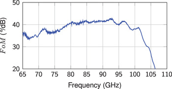
Fig. 11. Figure of merit.
In addition to the tunable effective permittivity of the LC layer, a part of the phase shift could be caused by undesired deforming bridge membranes as well. Therefore, the bridge membranes have been monitored through a microcope with a tight focal point, a deformation while tuning the phase shifter could not be observed.
C) Tuning speed
The tuning speed, i.e., the rise and fall time of the full tuning cycle, is governed by the LC behavior. It is defined in this work as the time necessary to tune the differential phase shift from 10 to 90% and 90 to 10% of the maximum differential phase shift, respectively. When the LC molecules rise from their initial orientation along the electrodes (no bias voltage and low permittivity value ɛ⊥, see Fig. 1(a)) towards the orientation along the field lines (bias voltage applied and high permittivity value ɛ‖, see Fig. 1(c)) this is referred to as rise time. The way back, when the LC molecules align themselves along the electrodes (with no bias voltage applied) is referred to as fall time. In order to measure the tuning speed of the phase shifter, the bias voltage was switched from 0 to 30 V and from 30 to 0 V, respectively. During the voltage switch, S 21 has been monitored at a single frequency using the VNA in a fast-CW mode. The time resolution of the VNA is about 1.6 ms.
The transient behavior of the phase shifter is shown in Fig. 12, it has been measured at a fixed frequency of 76 GHz and at 23°C. The measured tuning time is around 2 ms for increasing and 21.2 ms for decreasing the phase shift. The large difference between rise and fall time occurs, as the LC molecule alignment with an electrical field is much faster than the relaxation process of the molecules to their initial configuration along the surface.

Fig. 12. Rise and fall time measured at 76 GHz and 23 °C.
V. TEMPERATURE EFFECT OF TUNING SPEED
As described in the introduction, the dielectric properties of the LC are temperature dependent. Besides this, the alignment speed of the LC molecules depends on the temperature as well. With increasing temperature the viscosity of the LC mixture decreases and the molecules can be realigned faster; hence, the tuning speed of the phase shifter will increase with temperature.
The measurements of the temperature–dependent tuning time have been carried out on a phase shifter with a slightly different geometry. Unlike the dimension in Table 2 the MEMS bridge forming the cavity is 20% narrower and shorter. The structure was fabricated on 500 µm–thick fused silica. With a bias voltage of 30 V a maximum differential phase shift of 62° at 76 GHz could be achieved. The same measurement setup and techniques as described in the previous section are used, except that the waferprober chuck is equipped with a thermal management system and the measurements are carried out under a nitrogen atmosphere, in order to avoid problems caused by condensation water. The temperature is varied from 10 to 50 °C. Due to thermal expansion of different parts in the measurement system, the on-wafer probes need to be released before each temperature change and re-contacted before the next measurement. The bias voltage is altered between 0 and 25 V. Each measurement of the maximum differential phase shift is normalized individually to a range between 0 and 100%. This leads to a better comparability between the measurements at different temperatures, as differential phase shift may vary due the temperature–dependent material parameters of the LC.
The relative phase shift ΔΦ is measured over time and given in Fig. 13 for five different temperatures. Again the alignment of the molecules by the electrical field is much faster than the relaxation to the initial orientation along the surface. The tuning speed is strongly depending on the temperature. For 10 °C, which is quite close to the melting point of the LC at 5 °C, the tuning speed is very low and about two times slower than the tuning process at 23 °C. With increasing temperature the tuning speed increases strongly. According to Fig. 2, not only the tuning speed but also the dielectric losses of the LC increase. This leads to an increased insertion loss of the phase shifter at higher temperatures.

Fig. 13. Temperature dependency of rise and fall time measured at 76 GHz.
Figure 14 shows the measured maximum insertion loss as a function of the temperature. As it has been necessary to re-contact the probes for every measurement with slightly different contact forces and positions, the measured values probably include a relatively high inaccuracy. Nevertheless, a clear trend of increasing insertion loss with increasing the temperature can be observed.

Fig. 14. Temperature dependency of the insertion loss at 76 GHz.
VI. CONCLUSION AND OUTLOOK
The presented loaded line phase shifter consisting of 14 unit cells has shown a phase shift of 92° at 76 GHz with 2.4 dB insertion loss and an input matching of the order of −19 dB. The FoM varies between 35 to 42°/dB in the frequency range from 65 to 97 GHz.
The tuning time of the LC varactors measured at room temperature is about 2 ms for rising and 21.2 ms for falling phase shift. Measurements show, that the tuning speed can be increased by operating the device at a higher temperature, but this will increase the dielectric losses of the LC layer and decrease the tunability of the LC. Depending on the application, a trade–off between the three parameters tuning speed, dielectric losses and tunability needs to be found.
A particular novelty is the monolithic integration of LC varactors and MEMS technology, with the possibility to realize components and devices in a hybrid technology. The presented 90° loaded line phase shifter can be combined with a 1–bit 180° MEMS switch, to form a continuously tunable 0° to 360° reflection-type phase shifter. The hybrid phase shifter schematic is sketched in Fig. 15. Prototypes are under fabrication.

Fig. 15. 360° loaded line phase shifter.
Further technological work includes the development of a zero-level packaging solution, in order to make the device more resistant against environmental impacts.
ACKNOWLEDGEMENT
This work was supported by the European Union within the research project “ARASCOM”.
 Carsten Fritzsch received a diploma in electrical engineering from Technische Universität Darmstadt in 2008. Since August 2008, he has been working toward his doctorate degree at the Institute for Microwave Engineering and Photonics of the same university. His current research interests include reconfigurable antennas and components based on Liquid Crystals, as well as related fabrication and measurement technologies.
 Flavio Giacomozzi received his M.Sc. degree in mechanical engineering from the University of Padova, Padova, Italy, in 1982. Since 1983, he has been with Fondazione Bruno Kessler (FBK) [formerly the Centro per la Ricerca Scientifica e Tecnologica (ITC-IRST)], Trento Italy. From 1983 to 1988, he was involved with improvements of surfaces properties of materials. Since 1988, he has been with the Materials and Microsystems Division, FBK, where he was in charge of development of fabrication processes technological steps. Since 1996, he has been involved with the development of MEMS technologies and the realization of prototypes of several devices as sensors, capacitive microphones, and RF MEMS devices.
 Onur Hamza Karabey was born in Istanbul, Turkey, in 1983. He received the B.S. in electrical and electronics engineering from Middle East Technical University, Ankara, Turkey, in 2006 and M.Sc. degree in information and communication engineering from Technische Universität Darmstadt, Darmstadt, Germany, in 2008. He is currently working toward the Ph.D. degree in microwave engineering at the Institute for Microwave Engineering and Photonics at the same university. Since September 2008, he has been a Research Assistant with the Institute of Microwave Engineering and Photonics, Darmstadt University of Technology. His current research is focused on material characterization for microwaves and design of tunable passive microwave components and circuits based on liquid crystals.
 Saygin Bildik was born in Izmir, Turkey in 1983. He received his B.Sc. degree in Electrical & Electronics Engineering from Ege University, Turkey in 2005 and his M.Sc. degree in Electrical & Electronics Engineering from Izmir Institute of Technology, Turkey in 2008. Currently, he is working on reconfigurable antennas for the Ph.D. degree at Technische Universität Darmstadt, Germany. His research interests are mainly in reconfigurable reflectarrays based on Liquid Crystals.
 Sabrina Colpo received her M.Sc. degree in electronic engineering from the University Federico II, Naples, Italy, in 2005. In 2001, she was involved in the design and characterization of microstrip lines on micromachined silicon substrates with the Microwave Component Group (MCG)–DIMES Technology Centre, Technical University of Delft, Delft, The Netherlands. Since June 2006, she has been with the MEMS-Group, Fondazione Bruno Kessler (FBK) [formerly the Centro per la Ricerca Scientifica e Tecnologica (ITC-IRST)], Trento, Italy, where she is currently a Process Engineer involved with MEMS technology. Her current research interests include RF-MEMS switches, silicon capacitive microphones and the development process for kinetic inductance detectors (KIDs) on silicon.
 Rolf Jakoby was born in Kinheim, Germany, in 1958. He received the Dipl.-Ing. and Dr.-Ing. Degrees in electrical engineering from the University of Siegen, Germany, in 1985 and 1990, respectively. In Jan. 1991, he joined the Research Center of Deutsche Telekom in Darmstadt, Germany. Since April 1997, he has had a full professorship at TU Darmstadt, Germany. His interdisciplinary research is focused on RFID, micro- and millimeter–wave detectors and sensors for various applications, and in particular on reconfigurable RF passive devices by using novel approaches with metamaterial structures, liquid crystal and ferroelectric thick/thin film technologies. Rolf Jakoby is editor-in-chief of “FREQUENZ”, a member of the Society for Information Technology (ITG)of the VDE and a member of the IEEE societies MTT and AP. He is the organizer of various workshops, a member of various TPCs, and has been chairman of the European Microwave Conference 2007 and the German Microwave Conference 2011. In 1992, he received an award from the CCI Siegen and in 1997, the ITG-Prize for an excellent publication in the IEEE AP Transactions. He is a co-inventor of nine patents and has participated on eleven awards in the last six years.