I. INTRODUCTION
The antenna is one of the most important components of a wireless communication system. Planar antennas are very popular for wireless communication systems because of their ease of fabrication, integration, compactness, and low-profile characteristics. The emerging use of wireless systems requires more light weight and miniature antennas with low-cost, which can easily be integrated into small-size communication systems. The one way to reduce the size of planar antenna is to cut the slots and slits into the patch with respect to suitable feed point [Reference Chen, Wu and Wong1–Reference Chen3]. This reduces patch antenna size but degrades the antenna performance.
Reactive impedance surface (RIS) used as a substrate for planar antennas can miniaturize the size and considerably enhance both the bandwidth and the radiation characteristics of an antenna. The RIS substrate makes use of two-dimensional periodic metallic patches printed on a metal-backed high dielectric material. The RIS is also referred as meta-surface or artificial magnetic surface and used to provide a zero degree reflection phase for further improving the antenna radiations and miniaturization [Reference Mosallaei and Sarabandi4–Reference Mosallaei7]. A number of patch antennas inspired by the RIS structures have been suggested for size reduction [Reference Sarabandi, Buerkle and Mosallaei8–Reference Xu, Wang, Liang, Qi and Gao21].
In this paper a miniaturized coaxial feed bent slots loaded microstrip antenna (MSA) on a RIS substrate is proposed. Initially a traditional MSA is designed and optimized with good impedance matching. Bent slots are introduced in the patch to reduce traditional MSA size or resonant frequency [Reference Chen, Wu and Wong1]. Furthermore, a RIS is proposed and investigated for achieving further miniaturization. Miniaturization of bent slot loaded microstrip patch antenna is achieved by loading the antenna with RIS substrate. The RIS substrate is realized using two-dimensional (2D) cross-shaped metallic patches printed on a metal-grounded substrate. The simulation of antennas and RIS is carried out using CST Microwave Studio software package.
II. PATCH ANTENNA GEOMETRIES AND DESIGNS
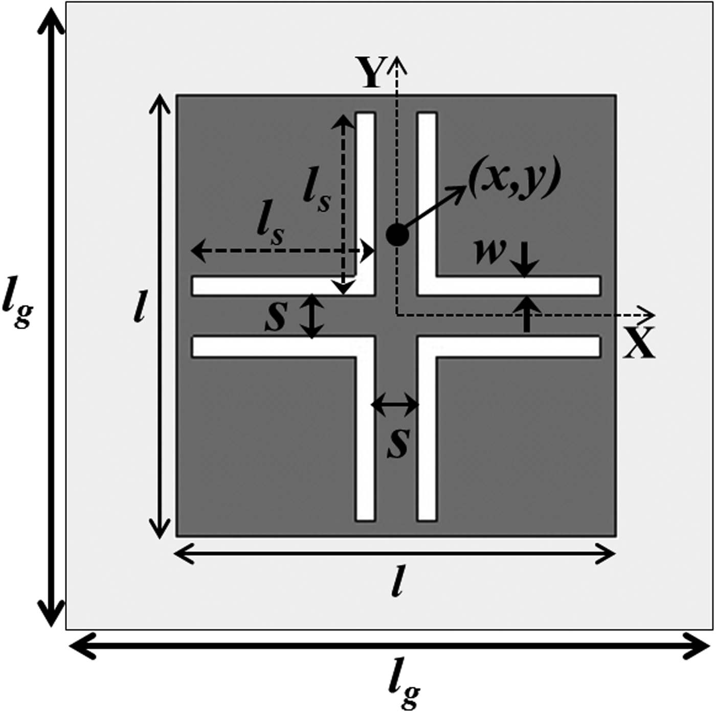
This section demonstrates step by step design of proposed antenna structure. A traditional patch antenna is designed and optimized for good impedance matching over a low-cost grounded FR4 dielectric substrate (ε r = 4.3, tan δ = 0.025) of height h = 4.5 mm and dimension (l g × l g) = 35 mm × 35 mm. The traditional patch antenna consists of a square patch of dimension (l × l) = 21.6 mm × 21.6 mm. To miniaturize traditional antenna, four bent slots of equal arm lengths l s are embedded in the square patch of a traditional antenna as shown in Fig. 1. Two arms of each bent slot of length l s and narrow width w (l s ≫ w) are aligned in parallel to the center lines of the square patch. The antenna design parameters are given in Table 1. By increasing the bent slots length, the fundamental resonant frequency of the slotted square patch antenna is significantly decreased. Figure 2 shows the proposed miniaturized patch antenna, which is designed by replacing the traditional ground plane of bent slots loaded patch antenna with a RIS structure. All antennas are excited using coaxial feed positioned at the point (x, y) from the patch center. In all antenna designs, thickness of copper is taken to be 0.017 mm.

Fig. 1. Bent slots loaded microstrip patch antenna over a traditional ground plane.
Fig. 2. Configurations of the proposed bent slotted patch antenna loaded with the RIS structure: (a) perspective view and (b) side view.
Table 1. Antenna design parameters (in mm).

The RIS layer consists of 5 × 5 cross-shaped metallic unit cell patch array printed periodically on a grounded low-cost FR4 substrate. The proposed antenna structure is a two layered dielectric geometry made up of FR4 substrate with thicknesses h 1 and h 2, respectively. The internal metallic layer is the RIS layer. A region on a RIS layer is removed for the coaxial SubMiniature version A connector so that the feeding probe does not contact directly with the metallic RIS patch. Antenna miniaturization is achieved by cutting bent slots in square patch and RIS layer as the meta-surface. In the next section, the characteristic of proposed RIS structure for bent slot loaded antenna will be investigated in detail.
III. PROPOSED RIS FOR BENT SLOTTED PATCH ANTENNA
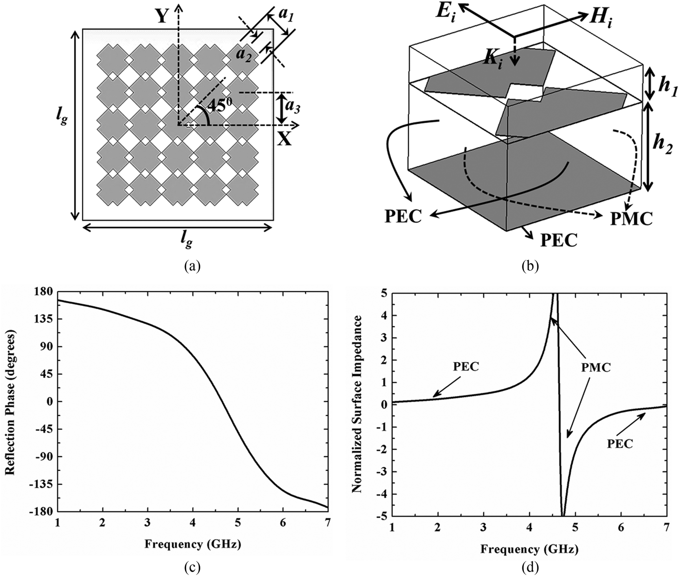
Figure 3(a) shows the top view of 5 × 5 cross-shaped patch array printed on a grounded FR4 dielectric slab. Like perfect electric conductor (PEC) or perfect magnetic conductor (PMC) surfaces, RIS can be designed to have the capability to reflect total power. RIS also have the ability to store magnetic or electric energy and tune a resonant antenna below its natural resonance frequency [Reference Mosallaei7].
Fig. 3. Proposed RIS: (a) top view of the 5 × 5 cross-shaped patch array forming RIS, (b) RIS unit cell enclosed by PEC walls in direction of E-field, PMC walls in the direction of H-field and illuminated by a normal incident plane wave (c) simulated reflection phase of the unit cell, and (d) normalized surface impedance of the RIS.
The design of a RIS for proposed antenna miniaturization is accomplished by 2D cross-shaped metallic patches printed periodically with period a 3 on a grounded dielectric. The unit cell of this RIS structure is first designed by exciting a plane wave to tune it between PEC and PMC boundary limits with an objective to achieve the best settlement between optimal performance and miniaturization factor. Figure 3(b) shows the unit cell simulation model of RIS. The unit cell is excited using a plane wave with a single-mode waveguide port on the top of it and the PEC and PMC boundaries are established around the cell structure. The reflection phase response for RIS unit cell structure is shown in Figure 3(c).
The actual cross-shaped metal patch parameters (a 1 and a 2) are altered to tune the operating frequency limit in the inductive RIS region, while keeping the overall size of RIS unit cell, as constant. Unlike the frequency selective surfaces, the periodicity of the RIS metallic patches is much smaller than the wavelength. The optimized values of RIS unit cell dimensions are given in Table 2. The RIS structure is equivalent to a parallel LC circuit with purely reactive impedance. From Fig. 3(d), the normalized surface impedance behaviors of the RIS structure indicate that below resonance the surface behaves inductively, as expected.
Table 2. RIS unit cell dimensions (in mm).

At low frequencies the RIS gives low impedance and acts as a PEC surface and at the resonance the reactance goes to infinity and the RIS behaves as a PMC. As a result, when the surface is combined with a capacitive radiating antenna element, the antenna starts radiating at a lower frequency.
Miniaturization of bent slot loaded square patch antenna is achieved by combining the reactive characteristic of the RIS with the capacitive (inductive) behavior of the patch antenna input impedance below its natural resonance to tune the resonance to a lower frequency range. The RIS provides a purely reactive impedance η = jν as in [Reference Mosallaei7], it reduces the mutual coupling between patch radiator and ground plane and henceforth shows a better performance and miniaturization factor than PEC and PMC ground planes. Figures 2(a) and 2(b) shows prospective and side view of proposed antenna loaded with a RIS substrate. The loading effect of bent slots and RIS in the traditional patch antenna will be described and discussed in detail in the next section.
IV. SIMULATED AND MEASURED RESULTS
As shown in Fig. 1, four bent slots are introduced in the traditional square patch MSA due to which the current on the patch and the field beneath the patch resonate from one edge of the patch and follow the longer path around the slots to reach the opposite edge. This reduces the resonant frequency or the physical size of the antenna. Figure 4 shows the current distribution on the patch surface at resonance for traditional square patch MSA and bent slots loaded MSA.
Fig. 4. Surface current distribution at resonance: (a) traditional MSA (b) bent slots loaded microstrip patch antenna over a traditional ground plane (l s = 9.55 mm).
For traditional patch without slots, the current takes primarily straight path from one edge to the other edge as shown in Fig. 4(a). From Fig. 4(b), due to the presence of the bent slots in square patch forces the current takes a much longer path. This clarifies the decrement in resonance frequency of the bent slotted microstrip patch antenna. From Fig. 4 it is also clear that an increase in the width of bent slots does not considerably increase path length of the current.
Figure 5 shows the simulated return loss for bent slot loaded MSA over traditional ground plane for different arm lengths (l s) of bent slots with a fixed optimized feed point for l s = 9.55 mm. As the arm length of bent slots is increased, there is a decrement in resonant frequency of antenna. Furthermore, it is apparent from this variation that path length of the current flow increases with increasing arm length of bent slots. The optimized value of arm lengths (l s) of bent slots is 9.55 mm, the reason to take l s = 9.55 mm rather than 9.7 mm is because of the limitation of fabrication machine.
Fig. 5. Variation of simulated return loss for bent slotted MSA over a traditional ground plane with arm length (l s) of bent slots (the feed point is (0, 3.8), which is fixed and optimized for l s = 9.55 mm).
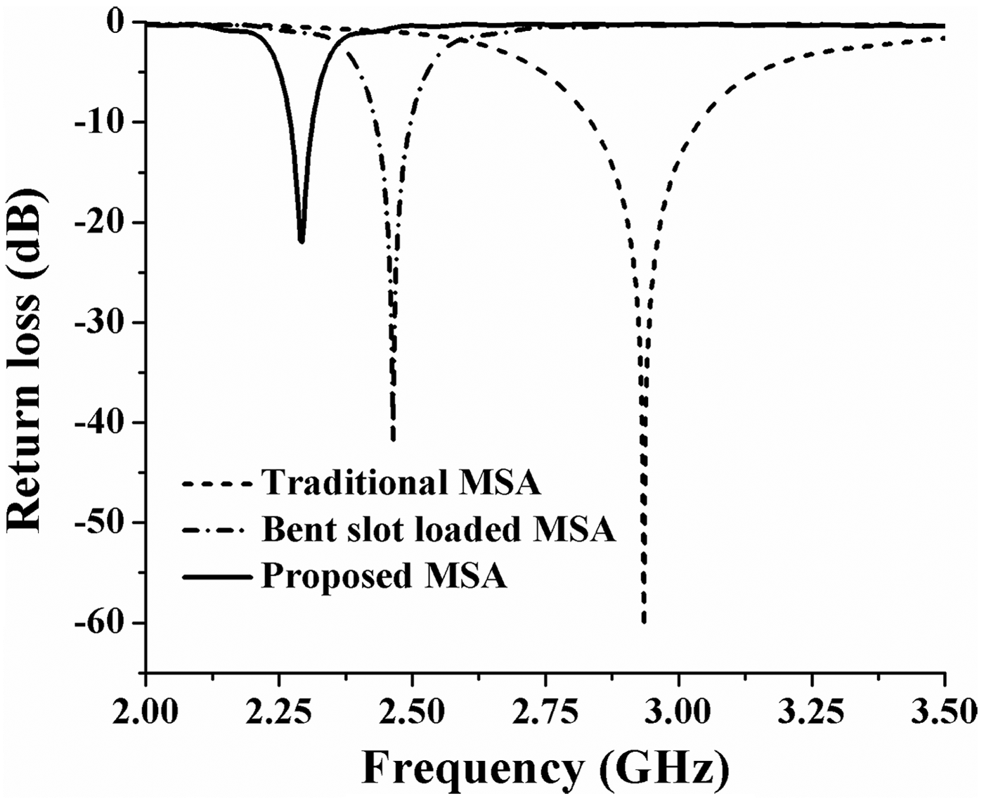
The simulated return loss for three different antenna designs is shown in Fig. 6. The designed antennas are with good impedance matching. From Fig. 6, it is clear that by introducing bent slots in the patch, the resonant frequency is downshifted from 2.93 to 2.46 GHz (i.e. 470 MHz) due to increment in the path length of surface current. The shift in resonant frequency of 16.04% can correspond to an antenna size reduction of ~32.54% at a fixed operating frequency or if a traditional patch antenna is designed to resonate at 2.46 GHz, the patch size would be 26.3 mm × 26.3 mm. The proposed antenna is a bent slotted MSA over a RIS substrate. The proposed antenna is made up by introducing RIS layer beneath the bent slotted patch and keeping the patch to ground plane distance constant. The proposed antenna is resonating at 2.29 GHz as compared with traditional MSA at 2.93 GHz due to the equivalent inductive reactance of RIS. The proposed antenna has a shift of 460 MHz in the resonant frequency as compared with traditional MSA, which corresponds to an antenna size reduction of ~42.15% at a fixed operating frequency.
Fig. 6. Simulated return loss graphs for proposed MSA, bent slotted MSA and traditional MSA.
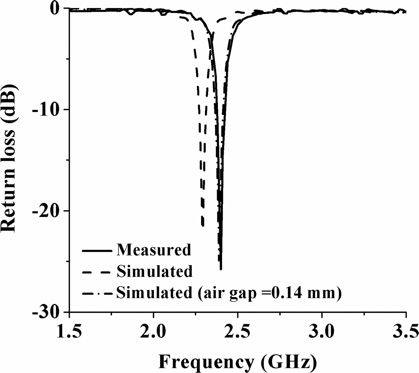
The proposed bent slotted MSA over RIS substrate is fabricated and measured for its return loss. The fabricated proposed antenna prototype and RIS layer is shown in Fig. 7. The antenna is fabricated using LPKF PCB prototyping machine. The measurement for return loss is done using Agilent vector network analyzer. The simulated and measured return losses for proposed antenna are compared in Fig. 8. There is a slight variation in the measured and the simulated return loss for proposed antenna structure. This variation in return loss is due to the fabrication tolerances, specially the effect of stacking layers of FR4 for achieving desired height of 4.5 mm and for inserting RIS layer in the antenna structure. Stacking of layers introduce a small air gap in multi-layered structure due to which the measured resonant frequency of fabricated proposed antenna is shifted to higher frequency range. If the fabrication is processed through standard multi-layered printed circuit board fabrication machine this variation in resonant frequency of proposed antenna may not be observed. To validate the effect of air gap introduced in stacking the layers a small air gap of 0.14 mm is introduced during the simulation of proposed antenna. The simulated return loss of proposed antenna with an air gap of 0.14 mm between the RIS layer and the bottom layer of antenna is in good agreement with the measured one as shown in Fig. 8. Minor ripples are observed in the measured return loss curve that might be due to the fabrication tolerances and reflecting environment because the measurement was carried out in a real environment with reflecting objects in the surrounding area. The fabricated proposed antenna is resonating at 2.39 GHz as compared with the traditional MSA at 2.93 GHz. The proposed fabricated antenna resonant frequency is 18.43% downshifted as compared with the traditional one which suggests a size reduction of 38.75% at a fixed operating frequency or if a traditional patch antenna is designed to resonate at 2.39 GHz, the patch size would be 27.6 mm × 27.6 mm. The measured 10-dB return loss bandwidth of proposed antenna is 2.26% (2.360–2.414 GHz).
Fig. 7. Fabricated proposed antenna prototype: (a) top view, (b) bottom view and (c) fabricated RIS layer.
Fig. 8. Measured and simulated return loss graphs of the bent slotted MSA over RIS substrate (proposed antenna).
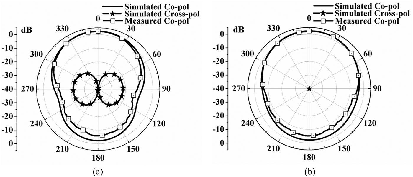
The measured and simulated radiation patterns of proposed bent slotted MSA over RIS substrate for both the principal planes (XZ Plane and YZ Plane) are shown in Fig. 9 at 2.39 GHz. There is a good agreement in the measured and simulated radiation patterns between −90 and 90° in YZ plane pattern and between −40 and 40° in XZ plane pattern. A minor difference is observed between measured and simulated radiation patterns which might be due to the presence of SMA connector assembly on the back of the antenna and reflecting environment. The patterns of proposed antenna are similar to the traditional antenna. The cross polarization level of proposed antenna in XZ-plane is less than −21 dB and in YZ-plane is less than −113 dB, means proposed antenna has very low level of cross-polarization. The performance comparison of different antennas is shown in Table 3. It is evident that the bent slotted patch antenna with and without RIS have comparatively lower gain, bandwidth, and efficiency with respect to the traditional antenna, which might be due to the higher quality factor of both the antennas, respectively. Since the antenna is electrically small a relatively lower gain is expected, as this is the limitation of miniaturization technique on antenna performance. The simulated gain and efficiency of proposed antenna are 2.4 dB and 53%, respectively, with an antenna size reduction of 38.75%.
Fig. 9. Measured and simulated radiation patterns of the bent slotted MSA over RIS substrate for both the principal planes at 2.39 GHz: (a) XZ Plane and (b) YZ Plane.
Table 3. Performance comparison of the antennas (the patch size is 21.6 mm × 21.6 mm and ground plane size is 35 mm × 35 mm, both are fixed for all antennas).

V. CONCLUSION
A miniaturized bent slotted patch antenna over a RIS substrate is presented and investigated. Bent slots are introduced into the patch for antenna size reduction. Further size reduction is achieved by replacing traditional substrate with a RIS consisting cross-shaped patch printed on a grounded low-cost FR4 substrate. The proposed antenna combines slotted and RIS technique for antenna size reduction. The proposed antenna is 38.75% miniaturized as compared with the traditional patch antenna and useful in S-band applications.
Saurabh Kumar received his B. Tech degree in Electronics and Communication Engineering from Uttar Pradesh Technical University, Lucknow (India) in 2008 and received his M. Tech degree in Digital Communication from Guru Gobind Singh Indraprastha University, Delhi (India) in 2010. He is pursuing his Ph.D. degree from Indian Institute of Information Technology, Design and Manufacturing, Jabalpur (India) since 2012. His research interest includes planar and microstrip patch antennas, artificial materials like meta-materials, electromagnetic theory, RF and microwave engineering, etc.
 Dinesh Kumar V. is an Associate Professor of Electronics and Communication Engineering at Indian Institute of Information Technology Design and Manufacturing (IIITDM), Jabalpur India. He received his Ph.D. degree in Electrical Communication engineering from Indian Institute of Science, Bangalore in 2005. He was a visiting foreign researcher in Japan from 2006 to 2009. Prior to this he was employed in Ministry of Communication and IT through Indian Engineering Services. His research interests include computational electromagnetics, microwave circuits, antenna and wave propagation, and photonics and optical communication.