I. INTRODUCTION
Circularly polarized (CP) antennas can receive all kinds of electromagnetic waves due to the insensitivity of the polarization matching between the transmitter and receiver. In this basis, the CP antennas have been applied to numerous wireless communication networks. Recently, the development of modern wireless communication systems has been brought greater interest in compact dual-band/multi-band CP applications [Reference Jinghui, Hongmei, Caitian and Wei1]. For example, single or dual-feed stacked patch antennas are reported to have dual-band/multi-band CP properties with a good impedance and AR bandwidth, [Reference Jinghui, Hongmei, Caitian and Wei1, Reference Nayeri, Lee, Elsherbeni and Yang2] at the expense of the height and cost. In [Reference Chen and Qing3], a single-feed multilayer CP microstrip antenna with S-shaped patch with dual-band CP operation is introduced for GPS applications. The slotted ground plane CP antennas for their advantages, like compactness and improvement in gain and axial ratio bandwidth are also studied widely [Reference Bao and Ammann4, Reference Shao and Chen5]. Single-feed single-layer slot loaded microstrip antennas are reported to have dual-band applications [Reference Chen and Yung6–Reference Yang and Wong9]. However, their impedance bandwidth is narrow which it is an inherent problem of microstrip antennas. For compensating this problem, two pairs of asymmetric ring-slots embedded on the ground plane are introduced for a single-band CP microstrip antenna [Reference Baik, Kim and Kim10]. The possibility of achieving a compact CP microstrip antenna based on arc-shaped slots is also investigated [Reference Chen and Qing11]. Some novel techniques are also included in literature for achieving circular polarization characteristics [Reference Ta, Park and Ziolkowski12, Reference Qing and Chen13]. In [Reference Yang, Caloz and Wu14], by merging and combining the near resonances of the half wavelength off-set parallel striplines a wider bandwidth is achieved based on mutual coupling for a phase-reversal antenna. In addition, it is possible to increase the bandwidth or enhance the properties of this technique with adding some dummy slots to the parallel off-set slots [Reference Yang, Caloz and Wu15]. This letter introduces a single-feed single-layer dual-band antenna for 1.5/2.5 GHz and a triple-band antenna for 1.02/1.36/1.43 GHz. The antenna design for each operation exploits the previously mentioned slot-loaded technique on the ground and also utilizes the complementary concept of the novel bandwidth enhancement technique which is stated earlier in this section. To demonstrate these concepts, the proposed dual-band CP antenna is designed and a parametric study was carried out. The antenna is simulated by high frequency structure simulator (HFSS) and time domain CST Microwave studio, then the performance is verified by the measurements.
II. ANTENNA GEOMETRY AND DESIGN
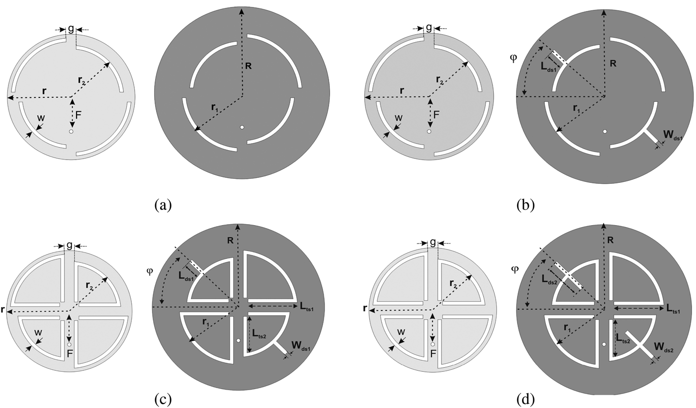
The proposed antenna designs for impedance bandwidth enhancing and compact dual-band/multi-band CP are depicted in Fig. 1. Figure 1(a) relates to the main antenna is composed of two printed metallic circular elements as ground plane and radiating patch where two pairs of asymmetric ring-shaped arc slots, with a narrow width w, are embedded on each side. The main antenna is fabricated on a low cost FR4 with ε r = 4.4, a loss tangent of 0.02 and a thickness of h = 1.6 mm. The antenna fed by a 50 Ω coaxial probe where the impedance matching is achieved by changing the ring slots width (w) and gap (g). The overall size of the structure is L sub × W sub mm2. Figure 1(a) exhibits the asymmetric ring-shaped arc slotted circular patch and ground plane with radius of r and R, respectively. The two asymmetric arc pairs are first centered to the reference point of the circular patch, then defined by a width of w and radius of r 1 and r 2, respectively, can be described as outer and inner ring-shaped arc slot radius. Finally, each arc, as depicted, is delimited by a gap of width g. The same configuration is exactly mirrored to the ground plane to take the advantage of mutual coupling to increase the bandwidth of a simple microstrip antenna. Using symmetric pairs of arc-shaped slots dictates a dual frequency operation with almost same radiation patterns and by adjusting them both TM 11 and TM 12 modes of circular patch can be excited properly. Also, it is reported that if two pairs are used, then, with a few modification of configuration, two orthogonal modes with equal amplitudes and 90° phase difference for CP operation can be excited for the both modes [Reference Hsieh, Chen and Wong7]. Another type of same modification is illustrated in Fig. 2(b). As shown, by extending a pair of dummy-slots with length of L ds1 and width of w ds1 out of the inner arc-shaped slots in the ground plane by an angle of φ, an antenna is proposed for dual-band CP operation. Also note that, these dummy slots can be placed anywhere to reach a CP radiation.

Fig. 1. Proposed asymmetric arc-shaped slot microstrip antennas for enhancing impedance bandwidth and dual/multi-band CP operation (a) antenna 1, (b) antenna 2, (c) antenna 3, and (d) antenna 4. Patch in lighter color on the top of substrate integrated with ground-plane in darker color placed at bottom.
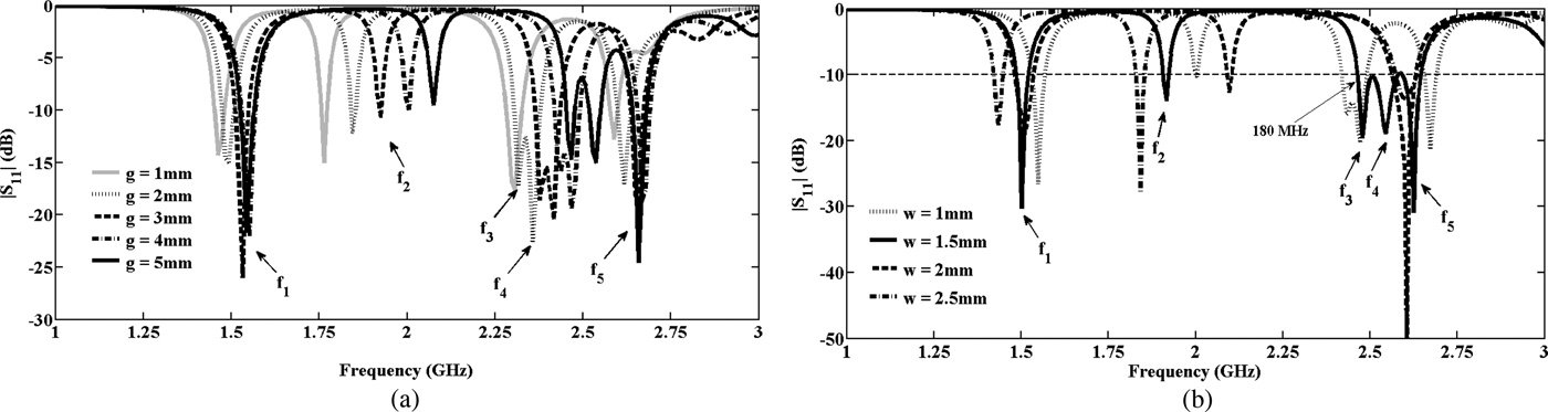
Fig. 2. Simulated |S 11| versus frequency for the stated values of Fig. 1(a): (a) for various slots gap (g), (b) for various slot widths (w).
It must be noted that the CP performance in both bands is controllable by optimization the features of these dummy slots. Utilizing the properties of asymmetric ring-shaped arc slots in both metallic plates can be realized when additional tuning slots with different length are etched in each end of an arc pair, as shown in Fig. 1(c). In the same figure, the length of tuning slots that are etched to the outer pair of ring slots, L ts1, must have a common ending point as the tuning slots which are embedded to the inner ring-shaped arc slots, L ts2. So, the length of tuning slots is also related to each other, determined by shifting method as L ts1 = L ts2 + 2w, is discuss in the next section. The antenna of Fig. 1(d) is similar to the previous one but the dummy slots are extended to modify the bandwidth performance of the antenna.
III. PARAMETRIC STUDY
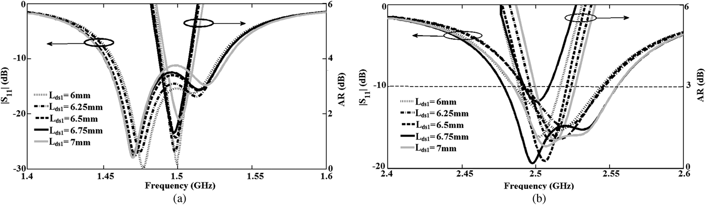
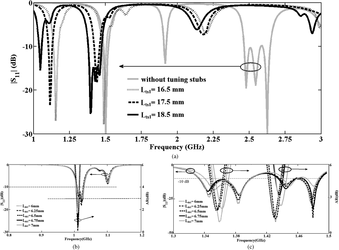
In order to enhance the impedance bandwidth of a single layer microstrip antenna and achieve a dual-band/multi-band CP operation, a parametric study has been carried out by HFSS software. All other parameters which have not been mentioned throughout this study are assumed to be fixed to the values of Table 1. The simulated return loss for different values of slots of antenna 1 is shown in Fig. 2. In Fig. 2(a), there are four types of resonant frequencies that are shown with arrows. As the amount of gap between the slots is increasing, the lower (f 1) and upper (f 5) resonant modes namely TM 11 and TM 12 are slightly changing as the main properties of the metallic parts remain constant. Meanwhile, the other significant resonant modes between these two frequencies are belong to inner patch radius, TM 21, f 2 around 2 GHz, and the combination of two resonant modes of asymmetric ring-shaped slots, namely f 3 and f 4. For f 3, it is obvious that increasing the amount of gap or decreasing length of slot will force it into the upper frequencies. This is also valid for f 4. As discussed in [Reference Yang, Caloz and Wu15], these modes are related to the coupling and combining of two resonances of each pair which are arranged to couple through a parallel metallic gap between them. The parallel metallic gap can be realized as a shunt capacitance which plays the main role in the mode coupling of two ring-slots. It is clear that the amount of this capacitance is changing due to the parameters of slots which leads to change in the amount of g. The coupling concept is completely explained in the corresponding reference [Reference Yang, Caloz and Wu15] and only the results are exploited here. It can be observed from Figs 2(a) and 2(b) that by proper selecting the values of g and w the impedance bandwidth of the main resonant modes of patch can be extended by merging and packing of more resonant modes around the frequency of interest. In other words, the higher-order mode of patch is fixed while the resonant modes of the slots are shifting toward this frequency. That is because the slots in the both plates have different length which leads to a complementary model of the prior one. This concept is fully utilized in the designs of the antenna 2 and 3 for increasing the bandwidth or achieving a multi-band CP operation in the lower band. It has been done by moving these resonances to the lower frequencies and couple_combine them with the fundamental resonant mode of the circular patch (f 1). Figures 3(a) and 3(b) show the effect of the length of dummy slots on the reflection coefficient and 3 dB axial ratio of the antenna 2 at the boresight. It is mentioned that the fundamental and the higher order mode of the circular patch are very important to form a dual-frequency operation and so as for a circular polarization. This extra pair of dummy slots changes the current distribution in the ground plane of the antenna at 1.5 and 2.5 GHz for antenna 2. Figures 4(a) and 4(b) show the current distribution around the patch and ground plane. As shown, the strongest current distribution is dispersed widely around the edges of the asymmetric arc-shaped slots in both bands, which can cause the meandering of the current paths on the patch or ground plane. However, it can be seen from Fig. 4(a) that the current flows a longer path near the edges and engages both inner and outer slots. On the other hand, the current flow is restricted around each slot in the upper band, as shown in Fig. 4(b). Adding a pair of dummy slots affects the both bands operations and slightly changes the currents length so that they show CP properties. The width (w) and length of tuning slots (L ts1, L ts2) without the effect of dummy slots were studied in Fig. 6(a). It means the tuning slots are directly added to the antenna 1. It was observed that by shifting the upper combined resonant modes toward the fundamental frequency the impedance bandwidth of the antenna increased. Also, it was found that other resonant frequencies appear around 1 GHz which are related to the current flow in the both inner parts and outer parts of the patch. This slots due to their symmetry form a CP radiation at around 1 GHz, as shown in Fig. 6(b). The reflection coefficient and 3 dB axial ratio of the antenna 3 with variation of dummy slots at 1.35 and 1.43 GHz are shown in Fig. 6(c). Figure 5 describes the current distribution of the antenna 3 at minimum axial ratio of each band. As shown, all the slots are charged and discharged repeatedly due to their length in a period of time so that the antenna always provides the 90 phase difference which confirms the inherently CP property of antenna 3 in the mentioned frequency bands. Design guidelines based on the simulation procedure is suggested as follows:
(1) The initial dimensions of the circular patch must be determined to operate in the desired frequencies, λ1 and λ5.
(2) Asymmetric ring-shaped slots lengths must be optimized to resonance between two frequencies of the patch. Length of each asymmetric ring-shaped slot is close to λ5/4 when they embedded to the boundary of the patch where λ5, the wavelength of upper resonance in free space is represented in Fig. 2. So, each asymmetric slot can help to meandering the path of current on the patch and forming a CP radiation, as shown in Fig. 4(b).
(3) For forming second CP radiation, a pair of dummy slots should be add to the slots with shorter length to be equal in length with the slots with longer length. Note that with adding dummy slots the sum of two ring-shaped slots will be equal to λ1/4.
(4) Tuning slots(L ts1, L ts2) must be embedded on the patch and connected to the asymmetric ring-shaped slots. Adjust the length of ring-shaped slots with tuning slots to resonance in frequency lower or equal to the lower frequency of the patch, f1. Apply the same design principle to the ground plane.
(5) Adjust the CP characterizes of the antenna with changing dummy slots to the form represented in Fig. 1(d). Make sure that both 3-dB AR bandwidth of around f 1 falls totally within the −10 dB return loss bandwidth.
(6) Check the possibility of forming a CP radiation in resonances lower than the first frequency of the patch. Optimize the overall structure and specially the tuning slots to reach a multi band function near 1 GHz.
Fig. 3. Simulated |S 11| and axial ratio versus frequency for the stated values of Fig. 1(b): (a) lower band (b) upper band.
Fig. 4. Current distributions of antenna 2 at (a) 1.5 GHz and (b) 2.5 GHz.
Fig. 5. Current distributions of antenna 3 at (a) 1.02 GHz, (b) 1.36 GHz, and (c) 1.43 GHz.
Fig. 6. Simulated |S 11| (a) without dummy slots for antenna 3, (b) with dummy slots at 1.02 GHz, and (c) with dummy slots at 1.36 and 1.43 GHz. Axial ratio is also included in (b) and (c).
Table 1. Optimized dimensions of the antennas of Fig. 1.
IV. EXPERIMENTAL RESULTS
Experimental results for each antenna have been carried out to demonstrate the performance of the designs. The photograph of top view and bottom view of each fabricated antenna and a comparison between measured and simulated return loss of the antennas plus their 3-dB AR measured at the boresight direction are shown in Fig. 7. The impedance bandwidth is measured with Agilent E8363C PNA network analyzer and axial ratio, gain and patterns of the experimental antennas were measured in our anechoic chamber in the laboratory building with a signal generator, antenna rotator and LG SA-970 spectrum analyzer. A frequency shift between the simulated and measured values is observed which is mainly caused by fabrication inaccuracy or soldering process. Figure 7(a) shows the measured and simulated return loss of antenna 1. The axial ratios of antennas were measured in boresight direction and at the centre resonant frequencies where the minimum axial ratio was obtained. As shown in Fig. 7(b), the measured impedance bandwidth and axial-ratio at the boresight direction of the antenna 2 are about 80, 30 MHz at the lower band and 100, 40 MHz at the upper band, respectively. The measured impedance bandwidth and axial-ratio at boresight direction of the antenna 3 which are shown in Fig. 7(c) are about 30, 8 MHz at the lowest band(around 1 GHz) and 90, 10 MHz around 1.39 GHz and 80, 10 MHz at the upper band (around 1.45 GHz), respectively.
Fig. 7. Photographs of the top and back view of the prototypes: (a) antenna 1, (b) antenna 2, (c) antenna 3, and (d) antenna 4.
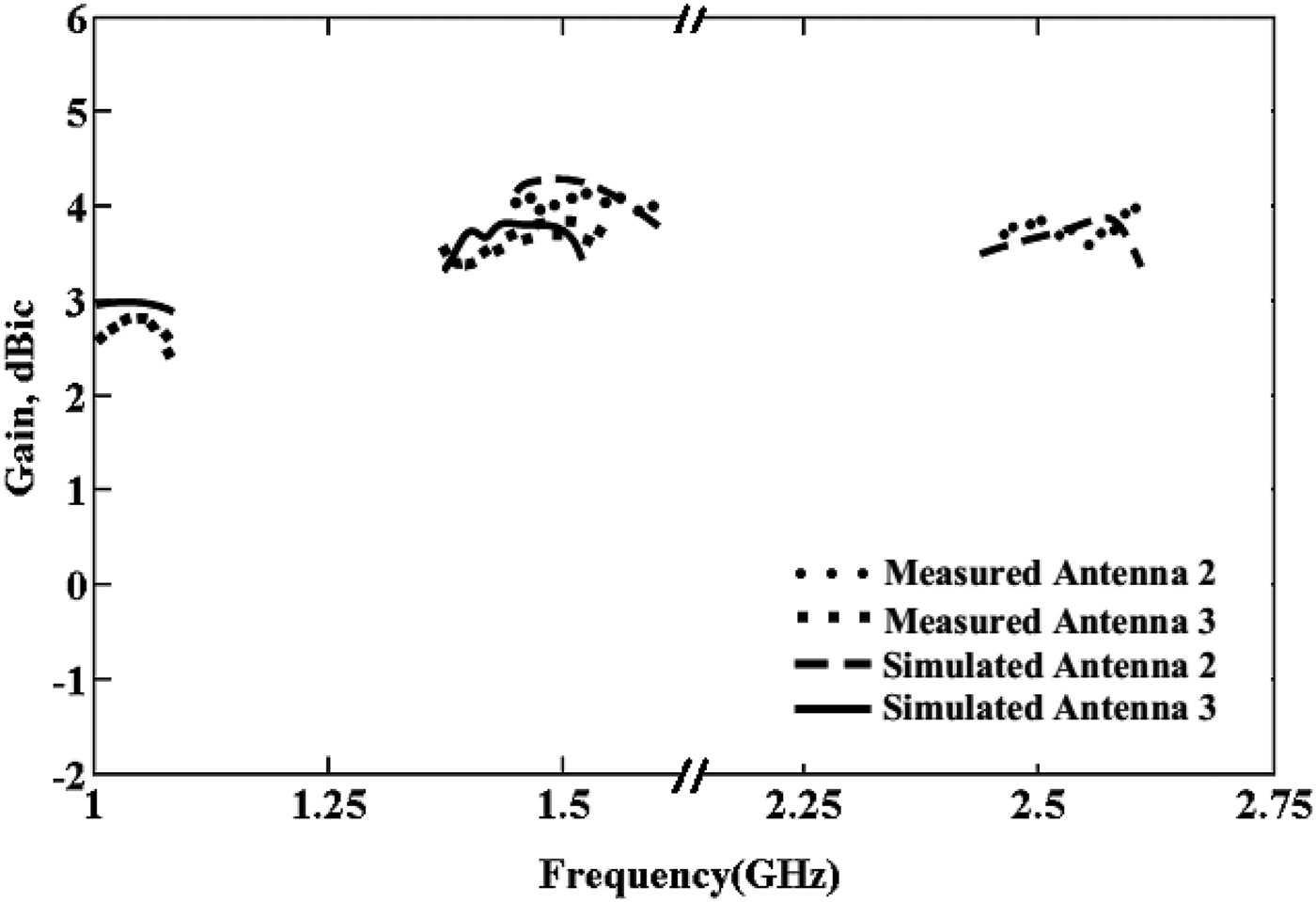
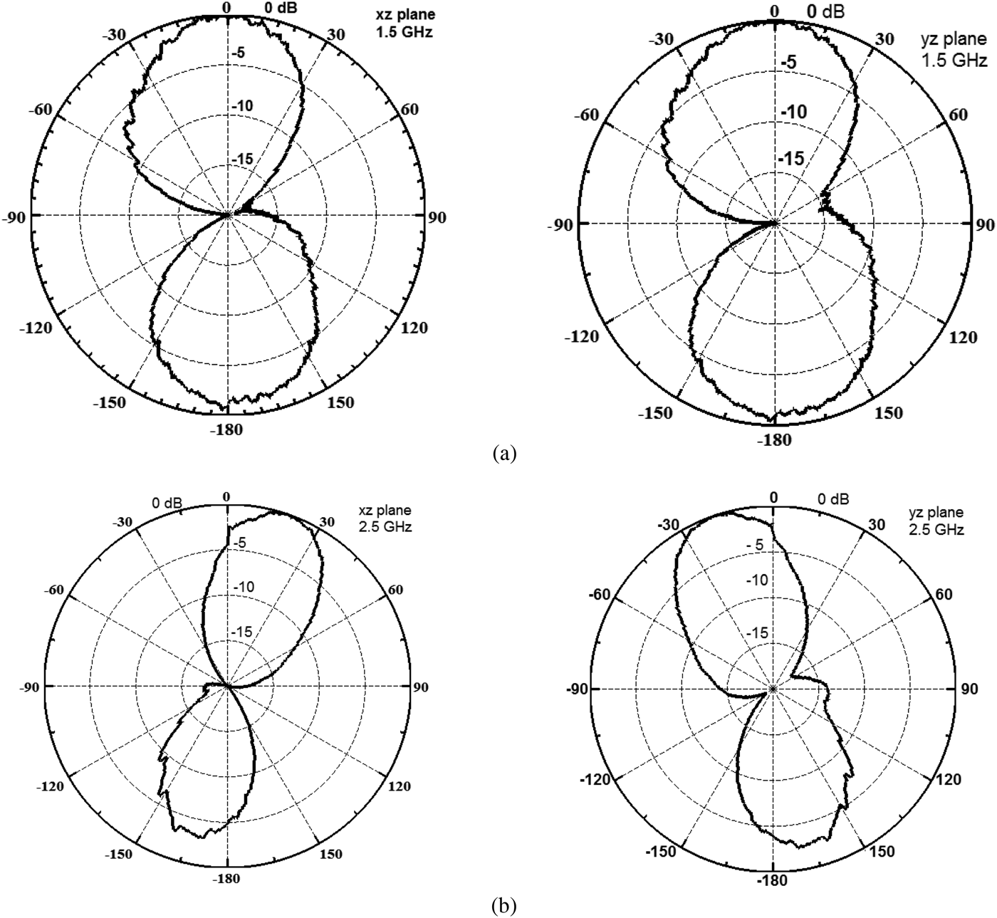
As shown in Fig. 7(d), the two upper bands of antenna 3 (1.36 and 1.43 GHz) are merged and modified into a wider bandwidth so the axial ratio for this antenna is not depicted. Also, the far field parameters of antenna 4 is not included. Figure 8 shows the measured and simulated CP gain at the boresight direction for both antenna 2 and antenna 3. The measured gain of antenna 2 is about 3.8 dBic at the lower band and at the upper band, it is around 3.6 dBic, with a variation of around 0.3 dBic within 3-dB AR for both bands. The measured CP gain of antenna 3 is around 2.8 dBic at lowest band and around 3.3 dBic at the upper bands. The simulated radiation patterns at the minimum S 11 of each band of the antenna 2 with both CST and HFSS software is shown in Figs 9(a) and 9(b). For antenna 2, a boresight CP radiation pattern is observed at the lower band; however, the patterns at the upper band show a 30° off-boresight radiation. This is primarily caused by both the presence of the ring-shaped slots in the configuration which form the CP properties of the antenna 2 and also due to antenna operation near the second resonance of the circular patch. It is found that the asymmetric current distribution of the higher order modes near the outer asymmetrical slot causes beam squint and pattern deterioration for the upper band. The normalized simulated radiation patterns of antenna 3 at minimum axial ratio of each band are exhibited in Fig. 10. It can be seen from Fig. 10 that the radiation pattern of the antenna 3 is modified owing to the performance of antenna near the first-order modes of the antenna. The current distribution is mainly flow in the inner parts of the patch while in antenna 2 the current is distributed between the asymmetric slots and outer edge of the patch. The measured radiation patterns for the antenna 2 at 1.5 and 2.5 GHz are plotted in Figs. 11(a) and 11(b) and for antenna 3 at around 1, 1.39, and 1.45 GHZ are depicted in Figs. 12(a)–12(c), respectively for both xz and yz planes.
Fig. 8. Measured and simulated gain of antenna 2 and antenna 3 at the boresight.
Fig. 9. Simulated radiation patterns of the antenna 2; (a) lower band (left), (b) upper band (right). The scale is 10 dB per division.
Fig. 10. Normalized simulated radiation patterns of the antenna 3 at: (a) 1.02 GHz (left), (b) 1.36 GHz (centre), and (c) 1.43 GHz (right). The scale is 10 dB per division.
Fig. 11. Measured radiation patterns of the antenna 2; (a) at 1.5 GHZ and (b) at 2.5 GHz.
Fig. 12. Normalized measured radiation patterns of the antenna 3; (a) at around 1 GHZ, (b) at 1.39 GHz, and (c) at 1.45 GHz.
V. CONCLUSION
A dual-band/multi-band single-feed single-layer CP microstrip antenna has been proposed, designed, fabricated, and tested. In contrast to previously reported dual-band/multi-band CP antennas, this letter introduces a new and simple design for dual-band/multi-band antenna by taking the advantage of the mutual coupling between ring-shaped slots to both enhance the impedance bandwidth and also draw the upper CP frequency to near the lower one. The other advantage of this new design in comparison to the other designs with same configuration is the simplicity of fabrication, wider impedance bandwidth in the upper band and later in the lower band, dual-sense CP capability and similar radiation patterns for the mentioned bands. The antennas configuration for each design have been implemented and tested separately.
ACKNOWLEDGEMENTS
The authors would like to thank the reviewers for their comments and suggestions, which helped to increase the quality and applicability of this paper.
Farzad Alizadeh was born on 1989. He received a bachelor's degree in communication engineering in 2012 from the University of Tabriz. He is currently working toward the M.Sc degree in RF and microwave engineering at Urmia University. His research interests include electrically small antennas, dual-band dual-polarized antennas, metamaterial designs and their applications.
Changiz Ghobadi was born on 1 June, 1960 in Iran. He received the B.Sc. degree in Electrical and Electronic Engineering and M.Sc. degree in Electrical and Telecommunication Engineering from Isfahan University of Technology, Isfahan, Iran and Ph.D. degree in Electrical-Telecommunication from University of Bath, Bath, UK in 1998. From 1998 he was an Assistant Professor and now is Associated Professor in the Department of Electrical Engineering, of Urmia University, Urmia, Iran. His primary research interests are in antenna design, radar and adaptive filters.
Javad Nourinia was born on 1969 in Iran. He received the B.Sc. degree in Electrical and Electronic Engineering from Shiraz University and M.Sc. degree in Electrical and Telecommunication Engineering from Iran University of Science and Technology, and Ph.D. degree in Electrical and Telecommunication from University of Science and Technology, Tehran, Iran in 2000. From 2000 he was an Assistant Professor and now is Associated Professor in the Department of Electrical Engineering, of Urmia University, Urmia, Iran. His primary research interests are in antenna design, numerical methods in electromagnetic, microwave circuits, filters and signal processing.
Mahdi Dadashi was born on 1989. He received a bachelor's degree in communication engineering in 2012 from the University of Tabriz. He is currently working toward the M.Sc degree in RF and microwave engineering at Urmia University. His research interests include design and optimization of microstrip antennas, dual-circularly polarized and multi-band antennas.
Rahim Barzegari received the B.Sc. degree in Electronic Engineering in 2003 and the M.Sc degree in RF and microwave engineering from Urmia University in 2014. His research interests include adaptive filters, reconfigurable antennas and antenna measurements.