I. INTRODUCTION
Recent years have witnessed an exponential growth in millimeter-wave circuits such as couplers, filters, and ortho-mode transducers (OMTs), to name a few. The latter is especially interesting for millimeter-wave applications, where two signals of opposite polarities can be transmitted or received using a single channel.
Although the OMT is a three-port device, from a physical point of view, it is nonetheless comprised four electrical ports. This is due to the fact that the input physical port receives or transmits two electrically orthogonal modes or signals, and can thus be viewed as two separate electrical ports. This is better understood when looking at Fig. 1, which shows the S-matrix (representing a four-port circuit such as the OMT which, electrically speaking, is a four-port circuit) and schematic representation of a typical ideal OMT circuit [Reference Uher, Bornemann and Rosenberg1]. Although both reflection and isolation should be minimized, reducing the latter is of utmost importance as, in the context of OMT's, it would signify cross-talk or cross-polarization between the two orthogonal modes.

Fig. 1. (a) The S-matrix, and (b) the schematic representation of an OMT circuit, assuming an electrical four-port OMT configuration. Numbers in blue: the (electric) port numbers. Dashed arrows: minimal cross-polarization interference.
A lot of research effort has been invested toward conceiving planar millimeter-wave components that can be seamlessly integrated within a complete communication system [Reference Wu, Deslandes and Cassivi2–Reference Patrovsky and Wu6]. The OMT, however, stands out as an exception owing to a multitude of reasons, chief among which is the original role of the OMT as polarization splitter. Because the signals to be separated by the OMT are of different polarization, the geometry of the OMT always contains two planes (mostly E and H planes). Alternatively, while a planar design is possible [Reference Uher, Bornemann and Rosenberg1], it is only feasible if septa are embedded in each of the output arms; in this case the septa would be aligned in different planes. In either case, it is a daunting task at millimeter-wave frequencies, given the minute lateral circuit dimensions that are in the order of less than one millimeter. Furthermore, a common problem encountered in millimeter-wave circuits design is the difficulty of conceiving them using micro-strip or co-planar waveguide, due to substantially higher losses and dimensional limitations associated with millimeter-wave frequencies [Reference Wu, Deslandes and Cassivi2].
Instead of the use of dielectric waveguides such non-radiative dielectric (NRD) waveguides were proposed [Reference Koul7]. Nevertheless, such waveguides have the problem of mechanical stability, which is easily circumvented using substrate integrated NRD (SINRD) waveguide, or the recently proposed, more compact image SINRD (iSINRD) guide [Reference Attari, Djerafi and Wu8]. The latter has the advantages, besides size compactness, of suppressing all even modes as well as possessing a versatile geometry. Those advantages encourage the use of the iSINRD guide in hybrid circuits. In this work, a planar iSINRD–substrate integrated waveguide (SIW) OMT is proposed, in which all sections lie in one plane only and no embedded septa are required. In Section II, the design principles are outlined. Simulated and measured results are then presented in Section III. The OMT is designed to operate at 94 GHz.
II. OVERVIEW OF ORTHO-MODE TRANSDUCES
From a physical perspective, OMTs are three-port power dividers whose operating principle resembles that of duplexers [Reference Uher, Bornemann and Rosenberg1]. However, from an electrical point of view, the OMT is a four-port device, since the input port of the OMT is always designed to support two orthogonal signals. Many OMT configurations and classes exist in the literature [Reference Uher, Bornemann and Rosenberg1], and their choice between them is subject to technical requirements and specifications, as well as fabrication limitations [Reference Uher, Bornemann and Rosenberg1].
The distinguishing feature of the OMT as a power divider is its ability to divide or combine two distinct signals of different polarization into or from separate ports with little cross-polarization interference between the two. Hence transmit and receive (or uplink and downlink) communication can take place simultaneously, since the transmit and receive ports are perfectly isolated. For this reason, OMTs are used in satellite communications and radar systems as well as radio astronomy applications. OMTs differ from diplexers in that they split and combine signals at the same frequency band, whereas diplexers typically handle signals of different frequencies [Reference Uher, Bornemann and Rosenberg1].
To support simultaneous uplink and/or downlink transmission of orthogonally polarized signals, an OMT is always designed with a common waveguide section that supports, at the same frequency, two signal modes of orthogonal polarizations. This common waveguide is always followed by a splitting section (sometimes called a turnstile junction) which precedes the two output ports (or transmit/receive ports in some applications), and its design principle varies depending on the application. This turnstile junction gradually separates the two combined signals into the ports that support their propagation. Therefore, the two signal ports are geometrically different.
In most OMT designs, the common waveguide is a square waveguide that supports the TE 10 and TE 01 modes, whereas the signal ports are rectangular waveguides that are geometrically the reverse of each other [Reference Uher, Bornemann and Rosenberg1]. A lot of geometrical manipulation is then required to gradually separate the two signals. In some designs, an H-plane waveguide is connected to the common E-plane waveguide to separate one of the two signals [Reference Uher, Bornemann and Rosenberg1, Reference Navarrini and Nesti9]. If a planar design is a strict requirement, septa can be introduced in the signal arms that help isolate the two signals [Reference Uher, Bornemann and Rosenberg1, Reference Chattopadhyay, Philhour, Carlstrom, Church, Lange and Zmuidzinas10], but this comes at the expense of significantly less bandwidth [Reference Chattopadhyay and Carlstrom11]. In either case, some degree of manipulation of the common waveguide is always required in order for the two orthogonal signals to be separated to their respective output ports with minimal cross-polarization interference. These manipulations become increasingly difficult at millimeter-wave frequencies.
A lot of research efforts have been invested to minimize the complexity of OMT design at millimeter-wave frequencies, such as the symmetric reverse-coupling 100-GHz OMT reported in [Reference Navarrini and Nesti9], and the 35-GHz OMT for correlation receivers, described in [Reference Peverini, Tascone, Virone, Olivieri and Orta12]. Despite the fact that they do not contain embedded septa, and no thickness tapering is required within a single plane, their design still requires the two output ports to be in orthogonal planes. Furthermore, their design is based on the rectangular waveguide which cannot easily implemented in planar circuits, and which exhibits more pronounced attenuation per unit length at higher millimeter-wave frequencies.
In the next sections, the traditional mechanical limitations of the OMT design at millimeter-wave frequencies (septa, thickness tapering, dual-plane design, and rigid waveguide design) are completely eliminated by virtue of intuitive use of a novel guiding structure as well as strategic implementation of orthogonal modes and boundary conditions.
III. A PROPOSED NOVEL OMT DESIGN
The only way to avoid thickness tapering of, or usage of septa in the output arms of the OMT, while still maintaining the planar architecture, is for the output OMT arms to be realized as different waveguides. Each of these different waveguides would then support only one of the two orthogonal modes, despite having the same thickness. This means that the common channel should then support both orthogonal modes at the same frequency, and the turnstile regions should be designed in a special way such that it can split the modes into their respective output arms without the need to resort to thickness tapering or implementation of septa.
The best planar alternative to the rectangular waveguide that can be easily integrated in planar circuits is the SIW. However, the above preposition would not be feasible with the SIW because it can practically support only the TE 10 mode; the orthogonal TE 01 mode would leak from the metallic via posts. Furthermore, although it is amenable to integration in planar systems, the use of the SIW does not eliminate the need for either septa or dual-plane design, since it is otherwise not possible to split the TE 10 and TE 01 modes, unless the thickness is changed in one of the output arms.
Fortunately, other guiding structures have been developed for millimeter-wave applications. One such waveguide is the NRD waveguide [Reference Koul7, Reference Bahl13], which is simply a dielectric strip placed between two metal covers, with the sides being regions of air; in other words, regions of parallel plates. Thus as long as frequency of operation is less than the cut-off of parallel plates modes [Reference Koul7], no modes are excited in the sides and the wave is well contained in the dielectric strip. Like the rectangular waveguide, its planar version is the SINRD guide [Reference Wu, Deslandes and Cassivi2], where the air regions are realized as perforation air via holes. Depending on the mode of operation, the more compact and versatile iSINRD guide can instead be used, which is half the size of the SINRD guide, thanks to a metal image plane that facilitates the size reduction [Reference Attari, Djerafi and Wu8, Reference Bahl13, Reference Al Attari14]. The set of modes supported by the three NRD variants are identical, except for the ones that are suppressed by the image metal plane in the iSINRD guide.
From a physical point of view, the only difference between the SIW and the iSINRD guide is the fact that the latter has only one metallic edge instead of two as in the SIW; the other side is a region of reduced permittivity (compared to that of the central guide). The NRD guide and its two planar versions are shown in Fig. 2(a), whereas the SIW is shown in Fig. 2(b).
Fig. 2. The 3D views of the (a) NRD guide (left), SINRD guide (center), and iSINRD guide (right) and (b) the SIW. Orange: metal covers, green: dielectric, white: air vias, and black: image metal plane of the iSINRD guide or metal via holes of the SIW.
The two guides, however, differ in the class of modes that they support. Although the SIW is technically limited to the TE modes only (TM modes are not supported since the side metal walls are not continuous), the iSINRD has a wider range of supported modes. Furthermore, it can support the fundamental TE 10 mode of the SIW, in addition to a host of other modes of orthogonal polarization, such as the LSM 10 mode. The two modes are shown in Fig. 3. It is important to mention that the TE 10 mode supported in the iSINRD guide is actually the second order of the TE 10 mode in the rectangular guide or the SIW (i.e. it is the TE 20 mode), because the image metal plane of the iSINRD guide suppresses the fundamental TE 10 mode [Reference Al Attari14], along with other symmetric TE modes. Also, while the TE 20 mode has an E component in the y-plane only, the LSM 10 mode has all three components. It is important to mention that the E z component of the LSM 10 mode must be zero at the center of the guide (i.e. x = 0 or at the metal image plane). For this reason, the LSM 10 mode continues to exist in the iSINRD guide despite the presence of the image metal plane [Reference Al Attari14].
Fig. 3. The cross-sectional front view of the E-field lines of the LSM 10 (left) and TE 20 (right) modes in the iSINRD guide. The × represent the E z component of the LSM 10 mode.
These facts about the LSM 10 mode and the TE 20 mode in the iSINRD guide facilitate the design of a planar OMT that has all its components lying in the same plane and that does not require any further modification of the output arms as would typically be required in traditional OMT designs. The detailed E-field equations of the two modes in the dielectric and side regions can be found in [Reference Koul7, Reference Al Attari14]. Further detailed analyses of the two guides, including analysis of the attenuation and propagation, can be found in [Reference Attari, Djerafi and Wu8] and [Reference Al Attari14].
IV. MECHANISM OF THE PROPOSED OMT
A) The geometry of the proposed OMT
The top and three-dimensional (3D) view of the proposed OMT is shown in Fig. 4. Its common channel is an iSINRD guide that supports the propagation of the orthogonal LSM 10 and TE 20 modes. The former mode is collected at an iSINRD guide output arm, whereas the latter is separated into an SIW output arm. The common channel and the output arms are separated by a tapered splitter region that facilitates the separation of the two modes into their respective arms. The splitter region does not have metal wall on either side. In other words, the splitter region is essentially an SINRD guide. Hence, there will be no radiation or diffraction from the central splitter region because, as aforementioned, radiation is suppressed in the side regions of the SINRD guide as long as the operating frequency is less than that of parallel plate modes (of the side regions). The parameter d control the length and width of the taper, whereas the parameter t controls the length of the metal side plane of the iSINRD guide common channel into the splitter region. In the special case where d = 0, the width of the taper equals the width of the iSINRD and the SIW; if they are equal. According to [Reference Al Attari14], the cut-off of the LSM 10 mode primarily depends on the thickness of the substrate, a, rather than the width which is mainly responsible for the bandwidth [Reference Al Attari14]. On the other hand, the cut-off of the TE 10 mode in the SIW depends only on the width, b [Reference Deslandes and Wu15]. Thus, to reduce the complexity of the design, the width of both guides ought to be equal. For an operational bandwidth centered at 94 GHz, based on Alumina substrate (ε r = 9.8, tanδ = 10−4 at 94 GHz [Reference Afsar16]), the optimum width for both modes is b = 0.6 λ g, while the substrate thickness should be a = 0.635 λ g [Reference Al Attari14]. This value ensures a single mode operation for both the LSM 10 mode (until 102 GHz [Reference Al Attari14]) and the TE 10 mode (until 150 GHz) Fig. 5.
Fig. 4. Top view of the proposed iSINRD–SIW OMT.
Fig. 5. A 3D view of the proposed iSINRD–SIW OMT with the lateral dimensions of each arm. White: air vias, orange: metal covers, black: metal planes, and green: substrate.
B) Mode separation
The OMT then works as follows. For the LSM 10 mode, since the E z component must be null at the metal plane, the LSM 10 mode cannot propagate into the SIW arm (port 2), and it will simply continue to the iSINRD arm (port 3). This is similar to the mechanism of the cruciform coupler described in [Reference Attari, Djerafi and Wu17], and in fact, for this mode, any value of d or t can be used, even d = t = 0. For the TE 20 mode, the splitter converts it into the TE 10 mode which, as mentioned earlier, is not supported by the iSINRD guide, since its metal side plan will suppress it. Therefore, it cannot propagate into the iSINRD guide output arm, and will instead propagate into SIW output arm where it is supported.
The parametric curves in Fig. 6, plot the transmission level of both modes as a function of frequency for different values of d, and confirm that d = 0.6 mm corresponds to optimum transmission. The value of t is then optimized using [18] and according to Fig. 7, t = d = 0.6 mm for optimum transmission and isolation. As is apparent, excellent separation of the two modes can be achieved with the above mechanism without introducing any septa or thickness changes, and without requiring different planes to separate the two modes. This is confirmed by the 3D E-field plot of the two modes shown in Fig. 8. Note that as established in [Reference Al Attari14], the air region in the iSINRD guide can be represented by a PMC plane to save simulation time.
Fig. 6. The relationship between the insertion loss and different values of d for (a) the LSM 10 mode and (b) the TE 10 mode.
Fig. 7. The effect of inset distance t on the S-parameters of (a) the TE 10 mode and (b) the LSM 10 mode. Black: transmission; red: reflection; blue: isolation.
Fig. 8. A 3D plot of the E-field of (a) the LSM 10 mode and (b) the TE 20 mode in the iSINRD–SIW OMT.
The different dimensions of the OMT established thus far can further be verified by simulating the two splitter segments shown in the insets of Figs 9 and 10. The first segment represents the feeding dual-mode arm of the OMT and half of the splitter region, whereas the second segment represents the other half of the splitter leading to the two output single-mode arms. The simulated S-parameters shown in Figs 9 and 10 indicate that the chosen dimensions correspond to optimum matching of the OMT sections and serve as a good verification to the splitter dimensions. Note, however, that those results are based on the assumption that the modes exactly in the middle of the splitter are pure LSM 10 and TE 10 modes. In reality, a hybrid of the two modes exists in the splitter due to their simultaneous feed to the input arm. The orthogonality of the two modes, however, ensures minimal interference, and the S-parameters in Figs 9 and 10 are thus valid for the hybrid case. Although other higher-order modes maybe excited, they are largely suppressed by the metallic walls of the iSINRD and SIW guides. They could further be suppressed if a metallic septum is introduced in the middle of the splitter region. Alternatively, the electromagnetic bandgap (EBG) structure mode suppression technique detailed in [Reference Cassivi and Wu19] could theoretically be employed. Those two mode suppression techniques, however, are not feasible at 94 GHz, and it suffices to use the metal planes of the iSINRD and SIW guides as mode suppressors.
Fig. 9. The S-parameter response of the LSM 10 mode in the (a) first splitter segment and (b) the second splitter segment. Insets: the E-field of the LSM 10 mode in each segment.
Fig. 10. The S-parameter response of the TE 10 mode in the (a) first splitter segment and (b) the second splitter segment. Insets: the E-field of the TE 10 mode in each segment.
C) Exciting the orthogonal modes
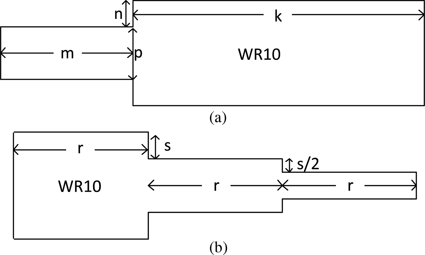
Given the high-target frequency (94 GHz), the use of microstrip or coplanar waveguide (CPW) excitation is impractical for the dimensions determined above. Alternatively, the tapered transition to WR10 has been the most frequently used excitation method of the LSM 10 and TE 10 modes in SINRD and SIW circuits, respectively [Reference Bahl13, Reference Cassivi and Wu19]. The schematic views and dimensions of the WR10 transitions for the two modes are shown in Fig. 11. The dimensions of the non-WR10 waveguide sections of the transitions were optimized using [18]. Note that, in the case of the LSM 10 mode, the WR10-waveguide transition has the same height but different lengths and widths. Conversely, for the TE 10 mode, the WR10-waveguide transition have the same width and length but different heights.
Fig. 11. (a) Top view and (b) side view of the WR10 transitions used to excite the LSM 10 and TE 10 modes respectively. k = 10.16 mm, m = 2.89 mm, n = 0.2175 mm, p = 0.835 mm, s = 0.1588 mm, r = 5 mm. Note: the diagrams are not to scale.
Since the two modes (and their WR10 feeding transitions) are orthogonal, the proposed iSINRD–SIW OMT cannot be fabricated as a three-port device. Instead, the OMT approach in [Reference Moldovan, Bosisio and Wu20–Reference Tao, Shen and Liu22] is employed, where the three-port OMT is fabricated back-to-back so that it has four ports; two of which act as feeding ports for the LSM 10 and TE 10 modes. Hence, conflict in mode excitation is avoided since each mode is being fed separately. The suggested four port OMT, and field plot of simultaneous feed, are shown in Figs 12(a) and 12(b), respectively. The “common channel” is thus an iSINRD guide that supports both (superposed) modes. In other words, actual OMT input port starts from the common channel, with mode separation into ports 3 and 4 taking place in the splitter on the right. The feed to the iSINRD arms is realized by tapering the substrate into the WR10 guide transition. On the other hand, the feed to the SIW arms is simply achieved by extending the substrate into the WR10 guide. Probe dimensions were optimized using [18]; lengths of the iSINRD taper and the SIW probe are 1 and 0.6 mm, respectively. The four-port OMT together with the feeding waveguides are shown in Fig. 12(c).
Fig. 12. The back-to-back four-port iSINRD–SIW OMT: (a) A top view of the back to back, four-port iSINRD–SIW OMT, and (b) Field plot of the four-port OMT, with simultaneous LSM 10 and TE 10 feed (top left corner). Notice the excellent separation at the output branches. (c) The four-port OMT together with the transition to the WR10-waveguide transitions.
D) Fabrication
The OMT is fabricated on Alumina (ε r = 9.8) substrate. As aforementioned, feeding of the LSM 10 and TE 10 modes is done by virtue of a tapered transition to WR10 waveguide as detailed above. The regions adjacent to the iSINRD arms were perforated using square (0.5 × 0.5 mm2) air vias. The dimensions were chosen to satisfy the non-radiating criteria of the LSM 10 mode, given by f x =  ${c / {\lpar 2a}}\sqrt {\varepsilon _2 } \rpar $, where f x and ε 2 are the cut-off of the parallel-plate mode in, and permittivity of, the side region, respectively [Reference Al Attari14].
All metallic walls are realized by the aluminum cavity metal. The reason being that metalizing via holes in alumina substrate with the MHMIC technique is not yet a mature process at our lab and is mostly unsuccessful.
Unlike the LSM 10 mode, which can still be contained in the dielectric despite some substrate perforation, the TE 20 mode requires an intense perforation that renders the iSINRD guide an iNRD guide. Otherwise, the TE 20 mode easily leaks into the side region. Therefore, an iSINRD circuit that involves operation with the TE 20 mode must have its sections that support the TE 20 mode realized as an iNRD guide. For example, the field plots in Figs 13(a) and 13(b) of an iNRD and iSINRD guide bends, respectively, illustrate this idea. It is clear from the two plots that the TE 20 mode would leak if the substrate perforation is involved, such as the case in an iSINRD guide bend. Conversely, an iNRD guide bend would contain the TE 20 mode well with no leakage. Therefore, air vias were avoided in the common central channel to prevent leakage of the TE 10 mode in the side region (See Fig. 12).
Fig. 13. 3D field plots in which: (a) The LSM 10 mode is well contained in the guide when the side region is purely air, and (b) The TE 20 mode easily leaks into the side region if it is perforated.
V. MEASUREMENT RESULTS
The fabricated prototype is shown in Fig. 14, together with the aluminum base within which the transition is realized. Measurements were made separately for the LSM 10 and TE 10 modes due to the vector network analyzer (VNA) being limited to two ports only. In other words, one input and one output ports were connected to the VNA at the same time, and loads were used to match the other ports. Prior to the measurements, standard thru-reflect-line (TRL) calibration was used to dembed the effect of the WR10 transition and the substrate tapers.
Fig. 14. The fabricated four-port iSINRD–SIW OMT.
Simulated and measured results of the OMT are shown in Figs 15(a) and 15(b) for the LSM 10 and TE 10 modes, respectively. In both cases, an insertion loss of around 1 dB is obtained at the frequency of operation (94 GHz), which includes the metal and dielectric losses (the latter being rather negligible given the low tanδ of Alumina, as verified in [Reference Koul7, Reference Afsar16]). A return loss of around 17 dB was obtained as well for both modes. The isolation for the LSM 10 mode is 30 dB) and that of the TE 10 mode is 17 dB at 94 GHz. The measured isolation level is very good and, in general, good agreement is observed between the simulated and measured results over the measured bandwidth which is around 6.5%.
Fig. 15. Simulated (S, color) and measured (M, black) S-parameters for (a) the LSM 10 and (b) the TE 10 mode, as well as the (c) cross-polarization interference between the LSM 10 and TE 10 modes.
For the two modes, the return loss is rather constant over the measured bandwidth, with an average of 20 dB for the LSM 10 mode and 17 dB for the TE 10 mode. On the other hand, the response of the cross-mode isolation is narrowband. This is because the cross-mode isolation is dependent on how well the splitter is able to sustain the conversion of each mode in the common channel to that which is desired to be exclusively supported by one of the output arms. Evidently, this process is frequency dependent, and can only be attained over a fraction of the measured bandwidth.
VI. CONCLUSION
This paper proposes a novel millimeter-wave planar OMT circuit comprised iSINRD guide and SIW, which are made in co-layered substrate. The design is motivated by the fact that the fundamental modes of the two waveguides are mutually orthogonal, and that the iSINRD guide can support the propagation of the TE 10 mode as well as the LSM 10 mode. Hence, with a correct choice of dimensions of the iSINRD guide and the SIW, a simple planar multi-waveguide OMT circuit can be conceived. Neither septa nor thickness tapering of the output branches are required in this setup. The OMT is fabricated as a back-to-back four-port OMT, in order to facilitate the excitation of both the LSM 10 and TE 10 modes. Measurements agree well with the theory, which confirms the validity of the proposed hybrid OMT.
The return and insertion losses have a rather flat response over the measured bandwidth compared to the cross-mode isolation. This points to the fact that the mode separation function of the splitter is frequency dependent, at least for the splitter topology proposed in this work. Further investigation of the splitter regions is thus required in order to improve the bandwidth of the cross-mode isolation. In addition, an in-depth modal analysis of modes in the splitter region is also considered for the future work.
Dr. Jawad Attari received his B.Eng. degree in Electrical Engineering from Sultan Qaboos University, Muscat, Oman, in 2004 and the M.Sc. degree in Communications Technology from Universität Ulm, Ulm, Germany in 2008. He recently obtained his Ph.D. degree in Electrical Engineering in 2013 from the École Polytechnique de Montréal. He won the first prize of the Student Design Competition of the IMS2012 in Montreal, and a Best Paper Certificate of Recognition at the EuMC, Nuremberg 2013. He is currently working as an RF Design at BlackBerry Product Development Center in Waterloo, Ontario, Canada, where he designs the complete RF Front-end of the BlackBerry smartphones. His current research interests include non-linear RF circuits design; envelop tracking techniques, as well as antenna design for smartphones.
Dr. Tarek Djerafi received the Dipl.Ing. degree from the Institut d'Aeronautique de Blida, Blida, Algeria, in 1998, the M.A.Sc. and Ph.D. degrees in Electrical Engineering from École Polytechnique, Montreal, QC, Canada, in 2005 and 2011, respectively. He is currently a Post-Doctoral Fellow with the École Polytechnique, Montreal. He has authored or co-authored more than 30 papers in journals and conferences. His current research interests include telecommunication antennas, beam forming networks, and radio frequency components design. Dr. Djerafi was the recipient of the NSERC Post-Doctoral Fellowship in 2011, selected for the Industrial R&D Fellowships Program in 2011, and for the FQNRT-CREER International Bourse in 2009 for his short-term Visiting Scholar in LAAS-CNES, Toulouse, France. He is currently serving as a Technical Reviewer for the IEEE-MTT, the IEEE Microwave and Wireless Components Letters Progress in Electromagnetic Research, IET Microwaves, and a Project Evaluator for the Romanian Research Council.
Prof. Ke Wu is professor of electrical engineering and Tier-I Canada Research Chair in RF and millimeter-wave engineering at the Ecole Polytechnique (University of Montreal). He holds the first Cheung Kong endowed chair professorship (visiting) at the Southeast University, the first Sir Yue-Kong Pao chair professorship (visiting) at the Ningbo University, and an honorary professorship at the Nanjing University of Science and Technology, the Nanjing University of Post Telecommunication, and the City University of Hong Kong, China. He has been the Director of the Poly-Grames Research Center. He was the founding Director of the Center for Radiofrequency Electronics Research of Quebec (Regroupement stratégique of FRQNT) for 2008–2014. He has also hold guest and visiting professorship at many universities around the world. He has authored or co-authored over 960 referred papers, and a number of books/book chapters and filed more than 30 patents.