I. INTRODUCTION
During the last decade, the unlicensed 9 GHz band about 60 GHz has been investigated for wireless communication and high data rate transfer applications. Several standards have been created for that matter such as IEEE.802.15.3c or WirelessHD ECMA and WiGiG, which are very close in terms of specifications. This work targets the frequency band of these standards from 57 to 66 GHz in Europe.
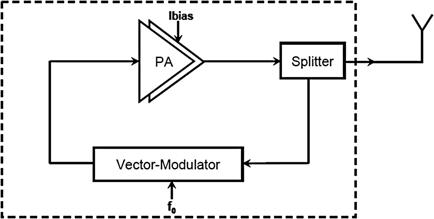
The key issues of transmitter architecture are the cost and the power consumption. A number of classical structures have been studied for this purpose including complementary metal–oxide–semiconductor (CMOS) designed structures which reduce the cost and the area [Reference Siligaris1]. This kind of usual CMOS transmitter can be further improved in terms of cost and consumption, thanks to a power voltage controlled oscillator (VCO) structure developed previously at 60 GHz in a 65 nm CMOS technology from STMicroelectronics [Reference Dréan, Martin, Deltimple, Kerhervé, Martineau and Belot2]. The principle of this original architecture consists of drastically reducing the number of blocks in comparison with common transmitter architectures like the heterodyne or homodyne architecture. As illustrated in Fig. 1, it consists of a loop composed of a 60 GHz CMOS power amplifier [Reference Moret, Deltimple, Kerhervé, Larie, Martineau and Belot3] in the direct path and a phase shifter in the feedback path. The phase shifter uses a part of the output signal, thanks to a power splitter which format this signal to fulfill the Barkhausen oscillating conditions, which correspond to a compensation of the gain in the direct path and the loss in the feedback, and a phase difference of 0° is required between the input of power amplifier and the output of the feedback loop. For this purpose, a vector modulator is used in the feedback loop in order to compensate the power amplifier phase and lead to oscillations.

Fig. 1. Power VCO diagram.
Phase-shifter topologies can be depicted in two categories: passive and active phase shifters. Passive phase shifters offer better bandwidth and linearity than active ones and have a very low power consumption [Reference Zhou, Qian and Yu4, Reference Tabesh, Arbabian and Niknejad5]. However, their losses generally increase with large phase shift range. To achieve the full 360° phase shift range with fine resolution, passive phase shifters are not the good candidates. Active phase shifter based on vector modulator allows 360° phase shift range with lower losses, nevertheless they consumes more power and occupies more area [Reference Tsai and Natarajan6, Reference Juntunen, Dawn, Laskar and Papapolymerou7] then passive solutions.
In this work, to compensate the phase bought by the power amplifier, the key point is the generation of all the phase shifting in continuous way. To do so, active phase shifter is preferred based on a vector modulator. A special care will be taken on the die area and power consumption.
The paper is organized as follows. First of all, the principle and schematic of the vector modulator (VM) is presented in Section II.A. Then, the mode of operation is described in the Section II.B. The VM was implemented in 65 nm CMOS technology from STMicroelectronics. Experimental measurements in the 55–66 GHz band are presented in Section II.C. Section III concludes the paper.
II. VECTOR MODULATOR
A) Circuit topology
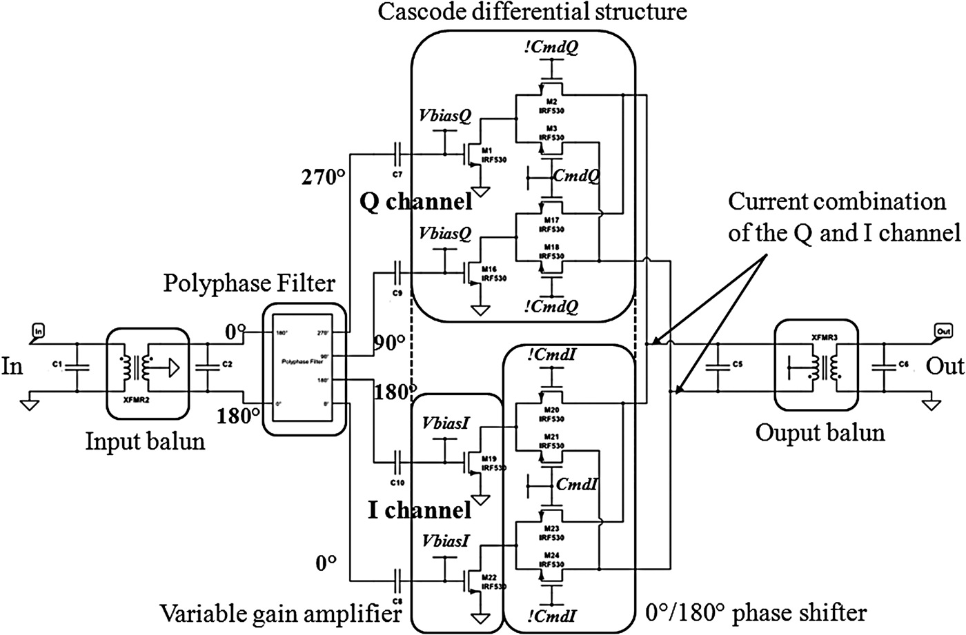
The VM shown in Fig. 2 consists of an input balun, a polyphase filter, two differential cascode structures, and an output balun. The input transformer provides the conversion of common mode to differential mode. The polyphase filter shown in Fig. 3 generates a phase difference of 90° between the two differential channels. Then, it generates from a differential signal (0° and 180°) two differential signals in quadrature the path in phase: I (0°, 180°), and the path in quadrature: Q (90°, 270°). The polyphase filter is composed of transmission lines. It was designed using electromagnetic simulations to generate 90° delay between the two differential output signals.
Fig. 2. Schematic representation of the vector modulator with bias and control voltages.
Fig. 3. Layout view of the polyphase filter.
Each path is composed of a variable gain amplifier and 0°/180° phase shifter. To realize these two functions, a cascode differential structure is implemented. The common-source transistors amplify the signal and the common-gate transistors are used to inverse the signal phase. Then the gain can be set in modifying the biasing voltages (VbiasQ and VbiasI) of the common-source transistors; and the phase inverting is controlled by the gate voltage of the common-gate transistors: CmdI, !CmdI, CmdQ, and !CmdQ.
In the vector-modulator output, the I and Q paths are recombined in current to realize a vector sum, and then in voltage sent to a transformer to come back in common mode.
B) Principle of operation
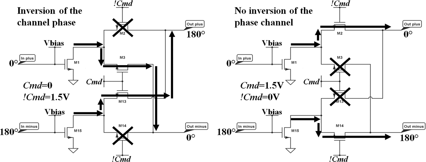
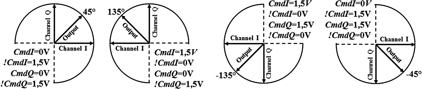
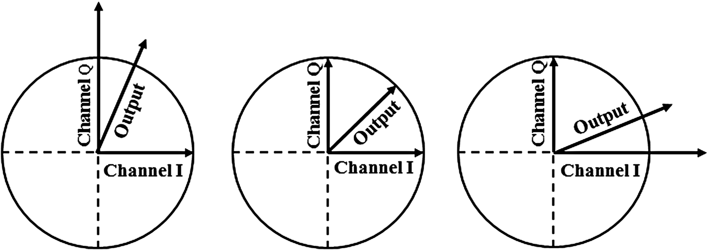
A first setting can be done, in choosing adequately the control voltages, to select one of the four phase quadrants: 0°/90°, 90°/180°, 180°/270°, and 270°/360°. To do so, the control voltages CmdI, !CmdI, CmdQ, and !CmdQ are set at 0 or 1.5 V. When CmdI is set at 1.5 V (so !CmdI is set at 0 V), the I path phase is inverted as illustrated in Fig. 4. Reciprocally, when CmdI is equal to 0 V (!CmdI = 1.5 V), the I path phase is not inverted. It is same for the Q path with CmdQ and !CmdQ. Finally, in choosing correctly this four control voltages, one of the four quadrants can be selected as illustrated in Fig. 5.
Fig. 4. Schematic representation of the differential cascode structure.
Fig. 5. Selection of the VM phase quadrant.
Then a second fine setting can be done in modifying the biasing voltages VbiasI and VbiasQ to select accurately the phase in the quadrant beforehand selected. After the vector sum of the I and Q paths, all the phase shifts from 0° to 360° can be generated as illustrated in Fig. 6.
Fig. 6. Fine tuning of the VM phase shifting.
C) Experimental result
The vector modulator is fabricated in the STMicroelectronics 1.2 V 65 nm LP 1P7M CMOS process. Figure 7 illustrates the chip micrograph. It occupies an area of 748 × 1250 µm2 with radiofrequency pads. Depending on its configuration, it consumes from 17 to 42 mA under 1.5 V.
Fig. 7. Chip micrograph of the VM
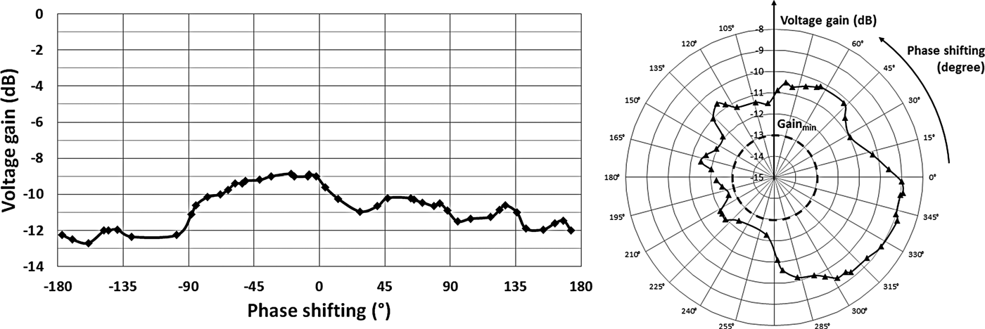
The voltage gain measurement in function of the phase shifting at 60 GHz is presented in Fig. 8. The vector modulator is able to generate all the phase represented in the polar circle with a voltage gain higher than −13 dB.
Fig. 8. Phase shifting and voltage gain of the VM measured at 60 GHz.
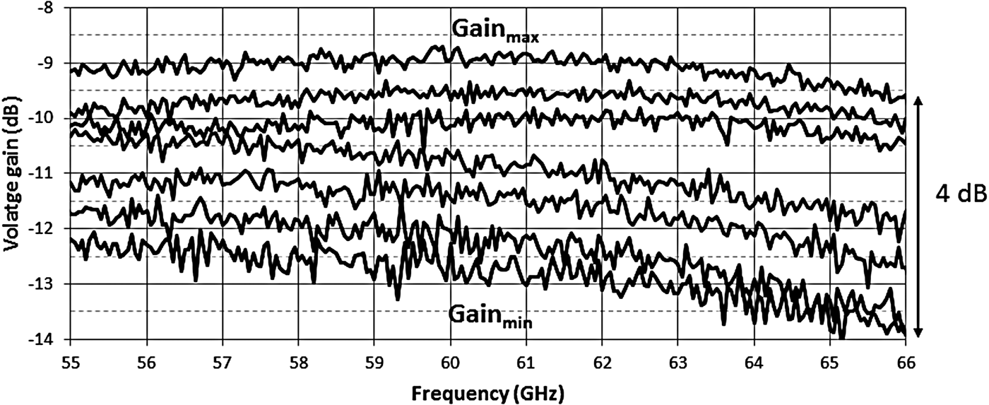
The vector modulator exhibits a stable voltage gain (±1 dB) on the whole measurement band from 55 to 66 GHz. It is comprised between −9 and −13 dB depending on his configuration as shown in Fig. 9.
Fig. 9. Voltage gain of the VM from 55 to 66 GHz.
Figure 10 shows the phase shift measurement depending on the frequency. The phase shifts of each quadrant are measured from 57 to 66 GHz. The VM is able to generate every phase from 0° to 360° over the 9 GHz band.
Fig. 10. Phase shift from 0° to 360° from 57 to 66 GHz.
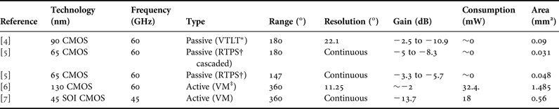
Table 1. 60 GHz phase shifter state of the art.
* VTLT: varactor-loaded transmission line.
† RTPS: reflective-type phase shifter.
‡ VM: vector modulator.
III. CONCLUSION
An active reconfigurable VM is implemented in 65 nm CMOS technology from STMicroelectronics. The VM is based on baluns, polyphase filter, and cascode amplifiers. Measurement results realized at 60 GHz show that this architecture offers a original solution to generate all the phase shifting from 0° to 360° in continuous way using control voltages. The voltage gain varies between −13 and −9 dB in function of the phase shift generated with a static consumption between 26 and 63 mW depending on its configuration. It was designed to fulfill the feedback loop needs of the 60 GHz power VCO and paves the way to a new way to realize emitters.
Boris Moret was born in Orléans, France, in 1990. He received the Engineering degree in Electronics from the Institute National Polytechnic of Bordeaux and his Master degree in Electronic from the University of Bordeaux in 2013. Now he is working toward his Ph.D. at the IMS Laboratory. His main field of interest is microwave PA design.
Nathalie Deltimple received the Ph.D. degree in Electrical Engineering from the University of Bordeaux, France, in 2005. She joined Bordeaux INP/ENSEIRBMATMECA and the IMS Laboratory in 2006, where she is presently an Associate Professor in the Electronics Department. Her main areas of research are the design of RF and millimeter-wave power amplifiers in CMOS and BiCMOS technologies for wireless communications and the development of integrated efficiency enhancement and linearization techniques. She is involved in the technical program committees of international conferences (IWS, RWS, NEWCAS) and serve as a reviewer for various journal (IEEE JSSC, TCAS-II, MTT, CSSP, MCWL, and AICSP) and conference (IWS, RWS, ICECS, NEWCAS, LASCAS, etc.). She is the In-charge of AMS&RF thematic inGDR SoC-SiP (CNRS) and Secretary of IEEE-CAS French chapter.
Eric Kerhervé received the Ph.D. degree in Electrical Engineering from the University of Bordeaux, France, in 1994. He joined ENSEIRB-MATMECA and the IMS Laboratory in 1996, where he is presently a Professor in Microelectronics and Microwave applications. His main areas of research are the design of RF, microwave, and millimeter-wave circuits (power amplifiers and filters) in silicon, GaAs, and GaN technologies. He is or was involved in European projects to develop silicon RF/mmW power amplifiers and BAW duplexer. He has authored or co-authored more than 190 technical papers in this field, and was awarded 23 patents. He has organized eight RFIC and EuMIC workshops on advanced silicon technologies for radiofrequency and millimeter-wave applications. He is involved in the technical program committees of various international conferences (ICECS, IMOC, NEWCAS, EuMIC, SBCCI, LASCAS) and he was the general co-chair of the international IEEE ICECS'2006 and IEEE NEWCAS'2011 conferences. He is the co-editor of Special Issues for IEEE-ICECS'2006, IEEE-ICECS'2007, and IEEE-LASCAS 2010. He was the associate editor of IEEE Transactions on Circuits and Systems II (TCAS II) for 2 years. He is the IEEE senior member and member of the IEEE-CAS, IEEE-MTT, and IEEE SSCS societies.
Baudouin Martineau received the M.S. degree in Microelectronics from the Sciences University of Bordeaux 1, France, in 2004 and the Ph.D. degree in Microwave and Microtechnology from the University of Lille, France, in 2008. He did his Ph.D. work at the Institute of Electronics, Microelectronics and Nanotechnologies (IEMN), Villeneuve d'Ascq, France and STMicroelectronics, Crolles, France. His Ph.D. thesis focused on the 65 nm CMOS SOI potentialities for millimeter-wave wireless applications. In 2008, he joined the Technology R&D department of STMicroelectronics, Crolles, France, as millimeter-wave and RF design engineer.
Didier Belot received the D.U.T. Electronique degree from the Institut Universitarire de Technologie, Grenoble, France, in 1982, and his M.S. degree from the Ecole Nationale Supérieure d'Electronique et de Radioélectricité de Grenoble, France, in 1991. In 1983, he joined the bipolar Device Characterization and Modelization group, Thomson Semiconductor. In 1986, he joined Thomson Etude et Fabrication de Circuits Intégrés Spéciaux, where he was involved in the digital CMOS design. In 1988, he worked on the design of high-speed ECL/CML data communication ICs at STMicroelectronics. In 1996, he moved to the radio-frequency design. He managed a design group involved in the development of circuits for mobile phones and local network standards in Central Research and Development, STMicroelectronics, Crolles, France. Presently, he works in the “Cellule Scientifique et Programmes” of Design Architectures & Embedded Software Division (DACLE division) in CEA-LETI, Grenoble.