


Introduction
The fourth (4G) generation technology was commercially deployed in Oslo, Norway, and Stockholm, Sweden in 2009, and since then was spread to the rest of the world. In March 2008, International telecommunication union (ITU) specified that the maximum peak speed of the technology should be 100.0 Mega bits per second (Mbps) for low mobility users like person traveling/walking on the road, and 1.0 Giga bits per second (Gbps) for high mobility users like persons traveling in car/train/aeroplane etc. The 4G technology uses frequencies in the range of 700.0, 850.0, 950.0, 1800.0, 1900.0, 2100.0, 2300.0, 2600.0, and 3500.0 MHz, etc [Reference Bliss and Govindasamy1, Reference Dahlman, Parkvall and Skold2]. The electromagnetic field, transmission lines, and wave theory is applicable while studying the effect of different characteristics of antenna technologies [Reference Benson and Benson3–Reference Jordan and Balmain5].
The 4G technology was designed to work over IP packet switching network, is able to dynamically share and use the network resources to support multiple users per cell. The 4G uses scalable channel bandwidth of 5.0--20.0 MHz optionally up to 40.0 MHz and has peak spectral efficiency of 15.0 bits/s/Hz in the downlink and 6.75 bits/s/Hz in the uplink. Also, the system spectral efficiency in indoor cases is 3.0 bits/s/Hz/cell for downlink and 2.25 bits/s/Hz/cell for uplink and having smooth hand-overs across heterogeneous networks. The 4G has some other features like use of multiple input multiple output (MIMO), turbo principle error-correcting codes, channel-dependent scheduling, link adaptation to spread a boon in the market for wireless users. Major advantages of 4G technology are that it has low latency data transmission, variable data speed from 100.0 to 300.0 Mbps, has scalable bandwidth, provides uninterrupted connectivity especially for video chats and conferences, better coverage, more secure and safer than previous technologies and affordable cost effective/pricing schemes [Reference Biglieri, Calderbank, Constantinides, Goldsmith, Paulraj and Poor6].
Apart from its pros, there were some cons which led scientists to switch to better technologies. Although, it offered uninterrupted connectivity, but to some regions its connectivity gets limited, and many users are annoyed by its glitches and bugs, and consume lots of battery power. Those who cannot access to 4G, have to switch to 3G/Wi-Fi while paying for the same amount as specified by 4G network plan, also users are forced to buy new devices to access 4G technology. Although, 4G long-term evolution (LTE) promised many features like serving 1 million base stations for outdoor and indoor applications, still it failed to satisfy the exponentially increasing demands of mobile and wireless users. Many researchers and mobile/wireless industries did their level best to increase data rate for worst case conditions, antenna gain, etc, but failed to do so due to growing demands of the user needs [Reference Hampton7,Reference Moradikordalivand, Leow, Rahman, Ebrahimi and Chua8].
The solution to problems of 4G is given by fifth generation (5G) technology. The 5G is built on the institute of electrical and electronics engineers (IEEE) 802.11 protocol and is aimed to speedup its data rate three times that of 4G. The mobile devices used with 4G can be modified to accommodate 5G antennas. The mobile company Xiomi and Samsung are working on the world's first 4G and 5G enabled mobile phones, which will work on 28 GHz (millimeter wave) and 3.5 GHz for 5G broadcasting, and 2.5 GHz 4G bands. Also, the 5G antenna can be assembled between LTE and wi-Fi antennas of 4G mobile phones [Reference Warren and Dewar9–Reference Boxall11].
The 5G technology is used by antennas with various combinations like implementing circular polarization (CP) or by forming single-user/multi-user and single-band/multi-band MIMO [Reference Li, Wang, Yuan, Liu, Zhao and Li12].
With the invention of wireless system, single input single output (SISO) came into the picture of growing market. It was typically less complex than MIMO as it used only one antenna in transmitter and receiver. It was used in satellite, radio, global system for mobile (GSM) communications systems. Although, it had some advantages but due to its drawbacks like high bandwidth, high interference, and range reduction in practical receivers, etc, its use is limited [Reference Rappaport13, Reference Schiller14].
MIMO is a more advance technology to solve the drawbacks of SISO. MIMO achieves better bit error rate (BER), delivers higher data rate due to transmission of multiple data streams/symbols, simultaneously using multiple antennas, and enhances coverage as compared to SISO. MIMO is the solution of the multipath propagation and is the vision of non-line-of-sight (NLOS) communication. MIMO also provides better results in respect of spectral efficiency, and capacity. Spectral efficiency of 4G technology is stated in table 1 for SISO and MIMO [Reference Molisch15, Reference Garg16]:
Table 1. Spectral efficiencies of SISO and MIMO

Spectral efficiency (bits/second/Hz) is calculated as per equation (1):
 $$\eta={R \over B}, $$
where η is spectral efficiency, R is data rate, and B is bandwidth of channel.
The capacity of SISO and MIMO are formulated using equations (2) and (3), respectively:
 $$C=B \log_{2}\left( 1+{S \over N} \right), $$
 $$C=\log_{2}\left( I_{N_{r}} +{P \over NN_{t}}HH^{\ast}\right), $$
 where  $I_{N_{r}}$ is identity matrix, P is signal power, N is noise power, N t, and N r are number of transmitting and receiving antennas, H is channel matrix, and
  $H^\ast $ is transpose of channel matrix, respectively.
The ITU passed a group of frequencies from 24.0 to 86.0 GHz for 5G technology [Reference Rodriguez17]. MIMO along with 5G technology demands very high bandwidth with reduction in its size due to high frequency, and also designed on microstrip patches [Reference Osseiran, Monserrat and Marsch18, Reference Yang, Chu and Mao19]. For the 5G most of the work is concentrated on the array designs for the gain enhancement and directional radiation patterns. The generalized equation of the two element array is given as (4):
 $$\eqalign{E_t & = E_1 + E_2 \cr & = \hat{a}_\theta j\eta \displaystyle{{kI_0l} \over {4\pi }}\left\{ {\displaystyle{{e^{-j[kr_1-(\beta /2)]}} \over {r_1}}\cos \theta _1 + \displaystyle{{e^{-j[kr_2-(\beta /2)]}} \over {r_2}}{\rm }\cos \theta _2} \right\}},$$
where E 1 and E 2 are the field radiated by 1st and 2nd elements, E t is the total field radiated by two elements, and β is the difference in phase excitation between the elements.
Above equation (4) can be modified as equation (5):
 $$E_{t}=E_{1}+E_{2}=\hat{a}_{\theta}j\eta\ {kI_{0}l \over 4\pi r}\cos \theta\left\{ 2 \cos\left[ {1 \over 2}(kd\cos\theta+\beta) \right] \right\}. $$
The total field of the array is equal to the field of a single element positioned at the origin multiplied by a factor called the array factor (AF), and is given in equation (6):
 $$AF=2 {\rm cos}\left[ {1 \over 2}(kd\cos\theta + \beta) \right]. $$
Similarly for N-elements AF is calculated by equation (7), and the normalized form of it is given by (8):
 $$AF=\sum_{n=1}^{N} e^{\,j(n-1)(kd \cos\theta+\beta )}, $$
 $$(AF_{n})={1 \over N}\left[ {\sin ( {N}/{2}\varphi \over \sin ({1}/{2}\varphi )} \right]. $$
The microstrip patch antennas are designed on various dielectric substrates like FR-4, Rogers RT Duroid, Taconic TLY-5, and polyimide, etc [Reference Kim and Tentzeris20]. The general formulas of width (W), length (L), effective dielectric constant (ε reff), variation in length (ΔL) due to fringing field, effective length (L eff) of a radiating microstrip patch antenna are given by equation (9) and equation (10) [Reference Malviya, Panigrahi and Kartikeyan21–Reference Stutzman25]:
 $$W={1 \over 2f_{r}\sqrt{\mu _{0}\varepsilon _{0}}}\sqrt{{2 \over \varepsilon_{r}+1}}={\vartheta _{0} \over 2f_{r}}\sqrt{{2 \over \varepsilon_{r}+1}}, $$
 $$L={1 \over 2f_{r}\sqrt{\varepsilon_{reff}}\sqrt{\mu _{0}\varepsilon_{0}}}-2\Delta L, $$
where f r is resonant frequency, μ0 and ε 0 are the permeability and permittivity of free space, ε r is relative dielectric constant,  $\vartheta _{0}$ is the free-space velocity of light.
The ε reff, ΔL and L eff are calculated by equations (11),(12), and (13), respectively:
 $$\varepsilon_{reff}={\varepsilon_{r}+1 \over 2}+{\varepsilon_{r}-1 \over 2}\left[ 1+12{h \over W} \right]^{-1/2}, $$
 $$\Delta L=0.142h{\left( \varepsilon_{reff}+0.3 \right)\left({W}/{h}+0.264 \right) \over \left( \varepsilon_{reff}-0.258 \right) ({W}/{h}+0.8)}, $$
 $$L_{eff}=L+2\Delta L. $$
Mode of microstrip patch antenna can be determined by using the formula (14):
 $$f_{m,n,p}={1 \over 2\pi\sqrt{\mu _{r}}}\sqrt{\left( {m\pi \over h}\right)^{2}+\left( {n\pi \over L}\right)^{2}+\left( {\,p\pi \over W}\right)^{2}}, $$
where, m, n, and p are variables to find the desired mode, and h is the height of the substrate.
The return loss (RL) in case of a single antenna/MIMO is given by equation (15):
 $$RL(dB)=10\,{\rm log}_{10} {1 \over {\rho}^2}, $$
where ρ is the reflection coefficient.
The characterization of multi-port/element or MIMO antennas for the diversity performance is done in terms of envelope correlation coefficient (ECC), mean effective gain (MEG), and total active reflection coefficient (TARC). The formulas of ECC (ρ), and MEG are given by (16), (17), and (18), respectively [Reference Malviya, Panigrahi and Kartikeyan26]:
 $$\vert \rho (i,j,N) \vert = {\left \vert \sum_{n=1}^{N}S^{\ast}_{i,n}S^{\ast}_{n,j} \right \vert \over \sqrt{\left \vert \prod _{{k}(=ij)} [1-\sum_{n=1}^{N} S^{\ast}_{i,n}S^{\ast}_{n,k}] \right \vert}}, $$
 $$MEG_{1}=0.5\eta _{1,rad}=0.5 [ 1- \vert S_{11} {\vert}^{2}- \vert S_{12} {\vert}^{2} ], $$
 $$MEG_{2}=0.5\eta _{2,rad}=0.5 [ 1- \vert S_{12} {\vert}^{2}- \vert S_{22} {\vert}^{2} ], $$
where S 11 and S 22 are reflection coefficients at ports 1 and 2, S 12 is port isolation, MEG 1 and MEG 2 are due to port 1 and 2 (in case of two ports only and is a generalized equation).
The another formulas of the MEGs are given by (19), and (20), respectively:
 $$MEG_{\,j}=\oint \left( {XPR \over 1+XPR} P_{\theta j (\Omega)} G_{\theta j (\Omega)} + {1 \over 1+XPR} P_{\phi j (\Omega)} G_{\phi j (\Omega)} \right), $$
 $$MEG_{\,j}={1 \over 2\pi}\int_{0}^{2\pi}\left[ {XPR \over 1+XPR} G_{\theta j}({\pi \over 2},\phi)+{1 \over 1+XPR} G_{\phi j} \left({\pi \over 2},\phi \right) \right]d\phi, $$
where XPR is the cross-polarization ratio. The value of XPR equals 0 dB for outdoor environment, and XPR equals 6.0 dB for indoor environment, respectively, and  $G(_\theta j)$ and
  $ G(_\phi j)$ are the gain parameters in azimuthal and elevation planes, respectively.
Similarly, TARC ( $\Gamma _{a}^{t}$) includes the effect of random variables and excitation angles at different ports of a designed multi-port antenna. TARC can be calculated for the designed multi-element/port or MIMO antennas using the equation given as (21):
 $$\Gamma_{a}^{t}={\sqrt{\vert ( S_{ii}+S_{ij} \;\ast\; e^{\,jq}) {\vert}^{2} + \vert ( S_{\,ji}+S_{\,jj}\; \ast\; e^{\,jq} {\vert}^{2}} \over \sqrt{N}}, $$
where θ is input phase angle, S ii and S ij are the input reflection coefficient and isolation between the ports, respectively.
The ECC, MEG, and TARC parameters for multi-port/element antenna can be obtained in terms of all the scattering parameters as well in terms of far-field characteristics. The ECC is an alternative to isolation parameter between any two ports or among all the ports of a designed antenna. The MEG is used to find the suitability of designed antenna under different environments e.g. isotropic, Gaussian etc, for indoor and outdoor applications. The TARC is used to find the active bandwidth and phase angles of the signals applied to the various ports. TARC curve resembles the shape of returnloss or isolation parameter for a particular combination of phase relations at ports.
Isolation enhancement techniques
Multi-port/element or MIMO antennas are designed in a compact space due to the requirement of the compact, portable, and wireless devices. This compactness may create the mutual coupling among the radiating elements of the designed antennas [Reference Talha, Babu and Aldhaheri27]. Various approaches like neutralization line [Reference Bang and Choi28, Reference Li, Shi and Liang29], defected ground structure (DGS) [Reference Das, Sharma, Gangwar and Sharawi30], inverted L-branches and slots [Reference Das, Sharma and Gangwar31–Reference Trifi, Sharawi and Shamim34], T-shaped metallic/slotted isolator [Reference Roslan, Kamarudin, Khalily and Jamaluddin35–Reference Imran, Farooqi, Khattak, Ullah, Khan, Khattak and Dar38], circular isolator [Reference Saxena, Kanaujia, Dwari, Kumar and Tiwari39], split ring resonator (SRR) [Reference Lim, Choi and Yoon40], ground modification techniques like partially extended ground (PEG) [Reference Malviya, Malik, Panigrahi and Kartikeyan41] and partially stepped ground (PSG) [Reference Li, Zhai, Ma, Liang, Yu and Liu42], cross-dipoles with baluns [Reference Huang, Li and Liu43], and radio frequency choke (RFC) as band stop [Reference Ardakani and Amiri44] are used to control the degrading effects of mutual coupling.
MIMO is also affected by the back lobe radiations due to the slotting in the ground. To solve the problem of back lobe radiation, a reflector plate is used behind the ground plane [Reference Malviya, Panigrahi and Kartikeyan45]. MIMO antenna with a reflector achieves high isolation, low cross polarization, high front-to-back ratio (FBR), and low side lobes [Reference Sarkar and Srivastava46]. The enhancement of FBR can also be done by feeding both identical antenna elements with equal magnitude current having 90° phase difference [Reference Li, Kang, Xu and Yin47].
MIMO antennas with space diversity, pattern diversity, and polarization diversity are used with monopoles/dipoles to control the effect of mutual coupling [Reference Paulraj and Kailath48–Reference Malviya, Panigrahi and Kartikeyan56]. The polarization diversity also controls the space required in MIMO implementation.
There are linearly polarized and circularly polarized (CP) SISO/MIMO antenna designed for stationary and moving users. The CP can be obtained using magneto electric (ME) dipole antenna [Reference An, Li, Fu, Ma, Chen and Feng57], rectangular slots apart by 90° etched at the center of a truncated rectangular patch, and also by diagonal feeding [Reference Toktas and Akdagli58].
MIMO with mathematically inspired generalized shape [Reference Chen and Chang59], MIMO with proximity coupled rings for capacitive effect [Reference Hakanoglu and Turkmen60], MIMO with semi-printed structure and fractals [Reference Yang, Yu, Zhou and Hong61], hybrid MIMO antenna with arrow-shaped monopole and a bended dipole with gap-coupled feed and L-shaped strips [Reference Minasian and Bird62], multi-layer MIMO [Reference Gao, Ma, Wang, Zhang and Parini63], multiband MIMO [Reference Li, Ban, Xu, Wu, Sim, Kang and Yu64] is a system of multi-element antennas like array antennas [Reference Komandla, Mishra and Sharma65]. Similarly, the narrowband and wideband antennas are designed for various applications.
MIMO with rectangular dielectric resonator antenna (RDRA) [Reference Malviya, Panigrahi and Kartikeyan66], aperture coupled cylindrical dielectric resonator (ACCDR), cylindrical DRAs (CDRAs) with metallic reflector are used to increase isolation [Reference Malviya, Panigrahi and Kartikeyan67], and are also used for multiband operation [Reference Malviya, Panigrahi and Kartikeyan68]. Some equations of the DRA are given by (22), (23), and (24) [Reference Luk and Leung69]:
 $$f_{r}={6.321c \over 2\pi \sqrt{\varepsilon _{r,eff}+2}}\left[ 0.21+0.36\left( {r \over 2H_{eff}} \right) + 0.02\left( {r \over 2H_{eff}} \right)^{2}\right], $$
where c is velocity of light, ε r,eff is effective dielectric constant, r is radius of CDRA, and H eff is effective height of antenna. The ε r,eff and H eff are obtained as:
 $$\varepsilon_{r,eff}={H_{eff} \over {H}/{\varepsilon_{Alumina}} + {H_{s}}/{\varepsilon _{sub}}}, $$
 $$H_{eff}=H+H_{s}, $$
where H and H s are the height of CDRA and substrate, respectively.
5G antenna designs
Various designs of 5G SISO/MIMO/array antennas [Reference Mak, Lai and Luk70] are described as follows in this section.
The lower spectrum of 5G bands is covered under the 3.3–4.2 GHz and 4.4–4.99 GHz. The higher frequency spectrum for 5G band covers frequencies like 24.25–27.5 GHz, 26.5–27.5 GHz, 26.5–29.5 GHz, 27.5–28.28 GHz, 27.5–28.35 GHz, 37.0–40.0 GHz, and 37.0–43.5 GHz which are deployed in countries like China, Korea, Japan, etc. Frequencies above 60.0 GHz are 53.3–66.5 GHz, 55.4–66.6 GHz, 56.6–64.8 GHz, 57.0–64.0 GHz and 57.0–65.0 GHz.
5G which is promising to deliver upto 1000 times as much data as today's networks, will also consume upto 1000 times as much energy as now. This consumption is becoming a hot topic to concern about. 5G small cell base stations are proposed to consume more than 50% of energy and can approach upto 800 watt with massive MIMO for high volume traffic. Hence, computation of power can play a vital role in energy efficiency of small cell networks. As computation power increases with the heavy traffic, transmission power reduces. Thus, there is a trade-off between these two. On comparing these two, former is small compared to latter, therefore, the energy efficiency investigation of small cell networks focuses on the optimization of transmission power at base station (BS). In this technology, power can be saved by BS sleeping scheme, where the RF's and transmitters of BS are closed during no traffic. As the number of antennas and bandwidths are increased, computation power also increases. Thus in 5G, computation power will playa more important role than transmission power, therefore both the powers should be considered while optimizing energy efficiency in 5G small cell networks [Reference Ge, Yang, Gharavi and Sun71].
Variety of dielectric substrates are available to design 5G antennas. While selecting the dielectric substrate material, its properties must be checked e.g. amount of surface wave production, loss tangent, permittivity, dispersion constant, anisotropy property, aging effect, temperature range, humidity effects, weight, elastic constant, solderability, mechanical strength, conformability, and cost etc [Reference Choudhary, Kumar and Gupta72].
The Polyethylene Terephthalate (PET) is commonly available polyester resin and also used in fibers. It is a nanocomposite in emerging applications. Its dielectric constant at 10.0 GHz is 3.2, dissipation factor is 0.002, surface resistivity is 1013Ohm/cm2, and volume resistivity is >1014 Ohm-cm [Reference Sima, Jiang, Peng and Sun73]. The Polydimethylsiloxane (PDMS) is a very flexible siloxane (Silicone) and most popular polymer. Its dielectric constant at 10.0 GHz is 2.7, dissipation factor is 0.0012, surface resistivity is 1014Ohm/cm2, and volume resistivity is >1015 Ohm-cm.These materials are the dielectric materials for the 5G and emerging antenna technologies. The PET and PDMS offer low value of dielectric constants when combined with other materials like glass microsphere (GM) [Reference Muhamad, Ngah, Jamlos, Soh and Ali74].
Microstrip patch antenna was fabricated and designed on polyethylene terephtalete (PET) of thickness 0.125 mm to cover X-band for 5G technology. The modified coplanar waveguide (CPW) feed with curtailed corners of patch were used to widen the bandwidth of the X-band region. The dimension of antenna was 60.0 × 75.0 mm2. The gain of 5.0 dBi and 38.0% efficiency was obtained in the frequency band of 7.0–13.0 GHz. The design is shown in Fig. 1 [Reference Tighezza, Rahim and Islam75].

Fig. 1. Microstrip patch antenna with PET substrate ©[Reference Tighezza, Rahim and Islam75]
When an array has a stacked structure of two shared aperture having sub-arrays orthogonally polarized, then it achieves wide bandwidth and stable gain in all the bands. Each pair of driven patches shared two parasitic patches by which the antenna achieves compactness. The slits and DGS are used to enhance the isolation. Rogers RO 4350 substrate with multiple layers were used with thicknesses of 0.762, 0.508, and 1.27 mm, respectively. The size of the antenna was 77.0 × 79.0 × 2.2 mm3. The different polarizations are achieved with the X-band as X-band horizontal (XH) and X-band vertical (XV); and with the Ku-band horizontal (KuH) and Ku-band vertical (KuV).The frequencies achieved in XH band is 8.3–11.3 GHz, in XV band is 8.7–11.5 GHz, in KuH band is 12.2–15.5 GHz, and in KuV band is 13.0–15.2 GHz, respectively. The horizontal and vertical components of polarizations in X-band have minimum of 200 MHz change in lower and upper frequencies. Similarly, the horizontal and vertical components of polarizations in Ku-band have minimum of 300 MHz change in lower and upper frequencies. The gain in XH band is 14.1 dB, in XV band 13.2 dB, in KuH band is 12.7 dB, and in KuV band is 12.7 dB, respectively. The isolation was >20.0 dB in all the bands. The design is shown in Fig. 2 [Reference Kong and Xu76].

Fig. 2. Antenna array (a) Array structure (b) Feed networks ©[Reference Kong and Xu76]
Substrate integrated waveguide (SIW) corrugated structures were used to design antennas instead of using waveguide feeder and grooves on a metallic plate. To analyze performance characteristics, antenna was made up of two and four grooves separately. At the bottom layer, transmission line was used to feed the antenna and in the middle layer, power was coupled to the patch. By employing grooves, high gain and narrow radiation patterns were achieved. For two groove antenna, gain was 11.3 dBi and for four grooves it was 12.8 dBi. Overall efficiency yielded >84.0% in the band. The frequency band for two grooves was 10.02–10.65 GHz while for four grooves, it was 10.09–10.7 GHz. Rogers 4003 having height of 0.508 mm was used for first and third substrates, while Rogers TMM4 having height of 3.175 mm was used for second substrate [Reference Honari, Mirzavand, Melzer and Mousavi77].
A flexible microstrip grid array antenna (MGAA) was inherited to design 5G antennas because of its ability to operate at high frequency and obtaining high gain. MGAA was designed using 1.9 mm thick polydimethylsiloxane (PDMS) substrate, while patch and ground plane were designed using conductive rubber material. MGAA consisted of 17 rectangular mesh cells having 24 radiating elements, thus enabling gain of 11.2 dBi at 15.5 GHz. The designed antenna covered the frequency range of 12.0–18.0 GHz. The total dimension of antenna was 60.0 × 60.0 × 2.4 cm3 [Reference Ramli, Rahim, Rahman, Sabran and Samingan78].
To utilize the device-to-device (D2D) communication, gain was increased in DRA array by steering the beam from −32° to +32°, achieving wide frequency range from 13.0 to 17.0 GHz. The resonant frequency was 15.0 GHz. The  $TE_{1\delta 3}^{y}$ mode DR was applied as driven element having narrow aperture in the ground plane to connect shorting pins. The DR having ECCOSTOCK HiK material was attached to ground plane using double sided duct tape having 0.058 mm thickness. The feeding network was fabricated on Duroid 5880 having thickness of 0.254 mm. The overall size of the antenna was 30.0 × 20.0 mm2. The achieved bandwidth was more than 1.3 GHz. The design is shown in Fig. 3 [Reference Shahadan, Jamaluddin, Kamarudin, Yamada, Khalily, Jusoh and Dahlan79].

Fig. 3. (a) Without DR (b) With DR ©[Reference Shahadan, Jamaluddin, Kamarudin, Yamada, Khalily, Jusoh and Dahlan79]
An antenna was made with a total of 16 rectangular meshes having short and long sides. The longer side acted as a transmission line but shorter side acted as a radiating element. If the length of the shorter side decreases below 9.84 mm, reflection coefficient increases. The FR-4 substrate having 49.0 × 58.0 × 1.6 mm3 size was used to design the compact grid array antenna for 13.8–15.9 GHz frequency range. At 15.9 GHz, gain and efficiency were marked as 14.4 dBi and 66.0%, respectively. The design is shown in Fig. 4 [Reference Yahya and Rahim80].

Fig. 4. Antenna with 16 rectangular meshes ©[Reference Yahya and Rahim80]
To investigate power density of antenna at two operating frequencies i.e at 15.0 and 28.0 GHz, two uniform linear patch arrays were used having 8 × 1 elements with a distance of λ/2 between them. On top of the phone chassis of dimension 140.0 × 78.0 mm2, an antenna array was mounted along with plastic box. Each patch element was 4.6 × 5.7 mm2 and 3.1 × 4.0 mm2 at 15.0 and 28.0 GHz, respectively. The design achieved more than 15.0 dB of isolation for both arrays. Two types of substrates were used in the design. The first substrate was Rogers 4003 for 15.0 GHz, and second substrate was Rogers 5800 for 28.0 GHz with thickness of 0.8 mm [Reference Zhao, Ying and He81].
Three identical sub-arrays of patch antennas were placed on the different sides of the antenna to attain 3D broad scanning coverage. Desired directions of beam were obtained by switching feeding to one of the 3 sub-arrays. Thus, a gain of higher than 10.0 dB was obtained in the frequency range of 21.0–22.0 GHz. A 1 × 8 linear array antenna was used, where each element was excited by equal magnitude. The center-to-center distance between each element was λ/2, having λ as the wavelength of 21.5 GHz. Total and radiation efficiencies were >80.0% and >95.0%, respectively. The Nelco N9000 substrate of thickness 0.787 mm was in the design, and the overall dimension of antenna was 110.0 × 55.0 × 4.5 mm3 [Reference Ojaroudiparchin, Shen, Zhang and Pedersen82].
A compact 8-element tapered slot antenna (TSA) was designed on Rogers RT 5880 covering 21.0–23.0 GHz frequency band. These elements were placed on the top portion of mobile's PCB to form an array. An antenna fed by hockey-stick balun, was designed to resonate at 22.0 GHz. The size of the antenna was 6.0 × 12.0 mm2, yielding the gain above 20.0 dB and efficiency of >95.0% [Reference Parchin, Shen and Pedersen83].
To increase the performance of an antenna, the resonator of conventional slot antenna was converted to air-filled slot loop structure. The narrow slot was made by a large copper metal surface having length equal to half guided waveguide and width equal to small fraction of λ. Thus, a metal ring resonator and a cubic slot were designed to nullify the sensitivity characteristics of the designed antenna. In 21.0–23.5 GHz frequency, gain was >5.5 dBi, while efficiency was >90.0%. The size of the FR-4 substrate was 10.0 × 5.0 × 0.8 cm3 [Reference Ojaroudiparchin, Shen and Pedersen84].
Two 4 × 4 array elements were implemented on the board, consisting of two stacked substrates. Top of upper substrate consisted of patch. Top and bottom of lower one consisted of U-shaped slot and micro-pin resonator plus hair-pin, respectively. The height of antenna and substrate were <1 and 0.2 mm (lower), and 0.787 mm (upper), respectively, whereas RO 4003C (lower) and RO 5880 (upper) were used as the type of substrates. The frequency range of the antenna array was 22.0–32.0 GHz with a gain of 19.0 dBi in the band. The design is shown in Fig. 5. The dimensions of U-slot and hair-pin resonators were obtained using the equations (25) and (26) [Reference Mao, Gao and Wang85]:
 $$L_{u1}+ 2\; \ast\; L_{u2}\approx {c \over 2f_{o}\sqrt{\varepsilon_{eff1}}}, $$
 $$L_{r1}+ 2 \;\ast \;L_{r2}\approx {c \over 2f_{o}\sqrt{\varepsilon_{eff2}}}, $$
where L u1, L u2, L r1, and L r2 are the dimensions of the U-slot and hair-pin resonators, respectively, f o is the resonant frequency, ε eff1 and ε eff2 are the effective dielectric constants, and c is the speed of light.

Fig. 5. Prototype of two arrays ©[Reference Mao, Gao and Wang85]
A 1/2 wavelength antenna element array achieved good beam-forming performance in H-plane. Millimeter-wave (MMW) circuit integrated substrate waveguide feeds the antenna element. The frequency band of 22.5–32.0 GHz having VSWR <1.45 and gain between 8.2 and 9.6 dBi were achieved in the design [Reference Malviya, Panigrahi and Kartikeyan86].
A wideband microstrip comb-line linear array antenna which worked in millimetre wave was operated over 28.0 GHz frequency and was made with Taconic TLY-5 substrate. The antenna consisted of 12 elements, reflection canceling slit structure, stubs, matching element and a via hole. Substrate's thickness and relativity permittivity were 0.508 mm and 2.2, respectively. The design provides bandwidth from 27.5 to 29.5 GHz with sidelobe levels in the range of only 6.167%. The distance between the elements is 4.076 mm. The stub matching is used to enhance the performance and impedance bandwidth of the antenna. The design is shown in Fig. 6. The length of the radiating element was found to be 3.38 mm using the following equation (27) [Reference Afoakwa and Jung87]:
 $$E_{L}= {c \over 2f_{r}\sqrt{\varepsilon_{re}}}-2\Delta E_{L}, $$
where ΔE L is the fringing field, f r is resonant frequency, ε re is effective relative permittivity and c is speed of light.

Fig. 6. Comb-line array antenna ©[Reference Afoakwa and Jung87]
A single dipole, 2 × 1 arrays, and 4 × 1 arrays were implemented and polarized vertically to achieve high gain, high radiation efficiency, wide bandwidth, and low cross-polarization. The gain of the combination was increased using parasitic element in-front of dipole as directors, while half power beam-width (HPBW) was increased by implementing directors as V-shaped. The via fence suppressed back-radiation, enhancing FBR by surrounding the dipole structure. Thus, by covering range of 24.0–32.0 GHz, dipole antenna, 2 × 1 and 4 × 1 arrays achieved a gain of 7.13, 9.83, and 12.61 dBi, respectively. The dimensions of electric dipole, 2 × 1 array, and 4 × 1 array were 10.0 × 24.2 × 4.9 mm3, 15.0 × 26.47 × 4.9 mm3, and 30.0 × 35.62 × 49.0 mm3, respectively. Rogers RO 5880 was used to fabricate electric dipole antenna having efficiency of 95.8%. The design is shown in Fig. 7 [Reference Halwagy, Mirzavand, Melzer, Hossain and Mousavi88].

Fig. 7. Electric dipole antennas ©[Reference Halwagy, Mirzavand, Melzer, Hossain and Mousavi88]
To reduce mutual coupling and enhancing isolation between the elements of 5G antipodal vivaldi antenna (AVA) array, 1 × 8 power dividers were used to feed the elements. On ground plane, multiple notch structures were added so that the isolation increases between them. Thus, an enhancement isolation, shift in frequency band from 24.65–28.5 GHz to 24.55–28.5 GHz, and enhancement in gain from 6.93 to 11.32 dB were achieved. The size of the antenna was 28.82 × 60.0 × 0.787 mm3 on Rogers 5880 substrate having thickness of 0.787 mm. The design is shown in Fig. 8 [Reference Zhu, Liu, Wen and Chen89].

Fig. 8. AVA array without coupling and with coupling reduced ©[Reference Zhu, Liu, Wen and Chen89]
A design was realized using three identical slot sub-arrays which controlled surface waves in order to have 3D coverage beam scan. Each sub-array had 8 elements separated with distance of 6.75 and 2.25 mm, respectively. The size of the antenna and substrate were 4.85 × 0.5 mm2 and 65.0 × 130.0 × 0.764 mm3, respectively. The Nelco N9000 PCB having relative permittivity of 2.2 and loss tangent of 0.0009 was used for substrate. The 25.0–30.0 GHz of frequency band was covered with isolation level of more than 12.75 dB, gain of 18.52 dBi, and ECC of <0.07 between two arrays. Total efficiencies of the three sub-arrays were 74.3, 68.0, and 72.2%, respectively [Reference Zhang, Chen, Syrytsin and Pedersen90].
A printed dipole angled at 45° was fed by an integrated balun which consisted of a 50 ohm microstrip line and a rectangular slot. An 8-element linear array was implemented to increase the beam-forming of antenna. The feed line was placed on top of substrate while dipole and ground plane on the back. Balun was used to match the impedance over broad frequency range, as it acted as microstrip-to-slot line transformer. The gain obtained by single antenna lied between 4.5 and 5.8 dBi and bandwidth of 36.2% in the frequency band of 26.5–38.2 GHz. While the antenna array achieved gain of 11.5–12.5 dBi and frequency band between 25.0 and 38.0 GHz. The arrays were fed by 8 ports. Mutual coupling was decreased by inserting microstrip stub between two printed dipoles with distance of 4.8 mm from center-to-center spacing. The antenna was fabricated on Rogers RT/Duroid 5880 substrate having thickness of 0.254 mm. The efficiency of >93.0% was achieved in the band [Reference Ta, Choo and Park91].
As 5G cellular network needs high bandwidth with low compact size and low design complexity, therefore DGS can be used for designing of 5G antennas. In this design, top surface of antenna consisted of radiating patch element with coplanar waveguide (CPW)-fed with T-shape, and the bottom part contained DGS having two iterations of symmetrical split ring slots. The isolation was enhanced by increasing distance between two adjacent patch elements. The size ofa single antenna was 12.0 × 12.0 mm2 on Rogers RT Duroid 5880 substrate having thickness of 0.8 mm. In the 25.1–37.5 GHz frequency band, ECC was <0.09. The gain was 10.6 dBi at 36.0 GHz and more than 80.0% efficiency in the band. The design is shown in Fig. 9 [Reference Jilani and Alomainy92].

Fig. 9. MMW antenna with DGS ©[Reference Jilani and Alomainy92]
In order to have advantages like low profile, wide bandwidth and high radiation efficiency, frequency selective surface (FSS) superstrate was selected to have high dense dielectric patch antenna instead of metallic patch. The antenna was fed by aperture-coupled technique. Thus, by employing FSS, gain of 17.78 dBi at 28.0 GHz and radiation efficiency of 90.0% were obtained. The frequency band of 26.0–30.5 GHz was obtained by placing 7 × 7 unit cells on the two sides of substrate. The square dense dielectric (DD) patch antenna, excited by coupling slot was placed above FSS layer. Rogers RT/Duroid 6002 ( ${\rm loss} \ {\rm tangent} = 0.0009$) was used to print DD patch, while bottom substrate was of Rogers RT 3010 (
 ${\rm loss} \ {\rm tangent} = 0.023$) material. Both substrates were 0.508 mm thick. The overall dimension of antenna was 32.0 × 32.0 × 1.8 mm3. The design is shown in Fig. 10 [Reference Asaadi, Afifi and Sebak93].

Fig. 10. Array antenna (a) Front, middle, and back (b) antenna prototype ©[Reference Asaadi, Afifi and Sebak93]
The Antenna-in-Package (AiP) design consisted of multilayer organic building substrates was designed to support both horizontal and vertical polarizations. The size of the antenna and substrate were 2.0 × 2.0 mm2 and 20.0 × 20.0 mm2, respectively, whereas organic build-up was used as a substrate. The covered frequency range was 26.0–36.0 GHz. At 30.5 GHz frequency, gain was 3.8 dBi [Reference Liu, Gu, Baks and Garcia94].
For enabling device-to-device communication in 5G network, a CP antenna was operated at 28.0 GHz frequency [Reference Wang and Du95]. The obtained frequency band was in the range of 27.5–28.35 GHz for 5G cellular network. An omnidirectional circularly polarized (OCP) antenna offered high gain, larger radiation coverage, and diverse communication links. Overlapped impedance bandwidth and 3 dB axial ratio bandwidth covered 2.2 GHz from 26.5 to 28.7 GHz. The height of antenna was 1.0 mm. At the center frequency of 27.6 GHz, gain was 0.7 dB. The dimension of substrate was 19.71 mm2 [Reference Lin, Ziolkowski and Baum96].
An antenna array having ground plane half of the size of Samsung Galaxy Note 4 was designed by stacking three substrates and a copper plate. To obtain broadband performance, an 8-way SIW feeding network based on Taylor distribution with broadband 4-stage unequal T-junction dividers plus cavity-backed antenna were designed to analyze its performance. On the upper side of substrate-1, antenna array was placed having 8 longitudinal slots to transmit wave from 1 to 2. This transmission of wave was done by coupling apertures of substrate-1 mounted on substrate-2 for the same purpose. Coupling apertures, cavity holes in Cu plate and radiating patches all constituted an 8-element cavity backed aperture-coupled antenna array. The gain of 14.9 dBi and efficiency of 75.0% were obtained in the frequency band of 26.5–29.7 GHz. The 0.508 mm thick Rogers 4350 B was used to fabricate the antenna. The design is shown in Fig. 11 [Reference Park, Shin and Park97].
Fig. 11. 8-element antenna structure ©[Reference Park, Shin and Park97]
A proximity coupled linear array antenna yielded a gain of over 13.5 dB by covering a frequency band of 26.5–28.92 GHz. The increase in bandwidth was due to linear manner of coupling from the feedlines above the substrate to the patches on the upper substrate and back down to the next feedline below and onwards. Both the substrates were made up of Taconic TLY-5 having thickness of 0.508 mm. The design is shown in Fig. 12. The number of elements were calculated as follows (28) [Reference Diawuo and Jung98]:
 $$D = dir + 10 {\rm log}(N), $$
where D is the directivity of the array, dir is the directivity of the single element, and N is number of elements in the array.

Fig. 12. Proximity coupled linear array antenna ©[Reference Diawuo and Jung98]
An antenna was designed on the concept of SIW slots. The antenna consisted of two SIW grooves and SIW slots which reduce mutual coupling in MIMO antenna. The SIW slot does not need any extra layer as required by SIW slit. The two MIMO antennas were designed to compare the performances based on the design parameters. MIMO 1 has dimension of 72.0 × 17.2 mm2 with a SIW groove, whereas MIMO 2 has 39.8 × 33.4 mm2 with SIW groove almost doubled than MIMO 1. The thickness of Rogers 5880 substrate was 1.575 mm. The gain of MIMO 1 was 9.5 dBi, whereas that of MIMO 2 was 11.0 dBi. An isolation level of higher than 20.0 dB, while ECC of lower than 0.02 were achieved for both MIMO antennas in the frequency band of 26.8–28.4 GHz [Reference Lin, Liu and Guo99].
Two Taconic TLY-5 substrates of thickness 0.508 mm were used for antenna having center frequency of 28.0 GHz. The lower substrate had 50 ohm microstrip line feeder which feeds the patch on the upper substrate. The length of feed varied directly with spacing between the patches and inversely with size of patches and with width of feedlines. The design achieved gain of 21.0 dBi over the frequency band of 26.9–29.21 GHz. The design is shown in Fig. 13 [Reference Diawuo, Jung and Jung100].

Fig. 13. Linear array antenna (a) front view (b) back view ©[Reference Diawuo, Jung and Jung100]
To attain left-hand and right-hand CP, two types of antenna elements were used. Each of the elements consisted of 4 layers, having substrate 1, 2, copper plate and substrate 3. A slot was etched in substrate 1 so that wave can transmit from 1 to 2. Similarly, slot of same dimension and location was etched in substrate 2. The circular drilling was done in copper plate and lastly on substrate 3. The desired CP can be obtained with a circular radiating patch. The antenna was printed on the Rogers 4350 B having 0.508 mm thickness. The size of single antenna was 70.0 × 63.5 × 2.2 mm3. It covered 3 frequency bands namely 26.9–30.9 GHz, 27.1–29.95 GHz, and 26.55–29.65 GHz. The 13.09 and 13.52 dBi gains were obtained for left-hand circularly polarized (LHCP) and right-hand circularly polarized (RHCP) modes, respectively. The design is shown in Fig. 14 [Reference Park and Park101].

Fig. 14. Antenna array (a)LHCP and (b)RHCP ©[Reference Park and Park101]
By using concept of traditional Wilkinson power divider, an antenna was modified to change the output power division ratio continuously. This power divider was used to feed the antenna to form a beam. To ensure flatness of power division, 2-varactor loaded L-shaped open stubs were connected to two branch lines of the device. Matching at different divisions were done by using two asymmetrically coupled lines at the output port and a stepped-impedance transformer at the input port. The Rogers RT/Duroid 5880 with 0.127 mm thickness was used as a substrate. The isolation was >10.0 dB over a frequency band of 27.0–29.0 GHz [Reference Abbas, Abbosh and Bialkowski102].
The RDRA antenna fabricated on RT/Duroid 5880 was fed by microstrip line in order to provide proper matching and ease in fabrication. As the number of elements increases, gain also increases but size of the antenna decreases. The gain of the antenna and array are calculated by equations (29) and (30), respectively:
 $$G=\eta\; \ast\; D, $$
 $$G=n\; \ast\; E_{o}\; \ast\; AF, $$
where G is the gain of antenna, E is radiated electrical field, E o is electrical field produced at center array by single DRA, n is number of elements, and AF is array factor.
To compensate between size and gain, 4 elements were used in the array. The spacing between the elements was 0.78λ to increase the gain while having acceptable side lobe level. The isolation in the frequency range of 27.0–29.1 GHz was obtained above 15.0 dB, while gain of 12.1 dB fulfilled the requirement of 5G application. The dimension of substrate was 11.0 × 12.0 × 0.254 mm3. The design is shown in Fig. 15 [Reference Nor, Jamaluddin, Kamarudin and Khalily103].

Fig. 15. Linear array DRA ©[Reference Nor, Jamaluddin, Kamarudin and Khalily103]
To compare the characteristics of metallic patch antenna and to enhance its performance, antenna was made with dense dielectric (DD) patch for 5G network. This DD PCB is easily compatible with radio frequency/microwave circuitry. The antenna comprised of two substrates. Four circular shaped DD patch radiators fed by 1-to-4 Wilkinson power divider were surrounded by electromagnetic bandgap (EBG) structure. The frequency band covered the range of 27.0–32.0 GHz, while gain and efficiency in the band were 16.3 dBi and 71.8%. The size of the RT 5880 substrate was 20.0 × 20.0 × 5.35 mm3 with thickness of 0.508 mm. The design is shown in Fig. 16 [Reference Haraz, Elboushi, Alshebeili and Sebak104].

Fig. 16. DD patch array antenna ©[Reference Haraz, Elboushi, Alshebeili and Sebak104]
In a cascode low noise amplifier (LNA), an inductor placed between common gate and source, was replaced by DGS because it reduces the overall silicon substrate area leading to overall reduction in the antenna size. It also provided good internal matching condition. Inductive and capacitive effects were easily attained in the antenna by implementing two rectangular slots of appropriate dimensions. Both of the rectangular slots were connected with the help of a small slot/gap. The inductive effect increased with the increase in current path, while capacitive effect increased because of charge accumulation in the slot. The peak-to-peak gain was obtained as 20.0 dB. The CMOS having thickness of 130.0 nm was used to fabricate antenna of dimension 0.27 mm2 for 27.2–29.0 GHz frequency application. The capacitance and inductance of DGS structure were calculated by equations (31) and (32) [Reference Luo, He, Wang, Chang, Huang and Yu105]:
 $$C_{DGS}={w_{c} \over Z_{o} \;\ast\; {g_{1}}}.{1 \over w_{o}^{2}-w_{c}^{2}}, $$
and
 $$L_{DGS}={1 \over w_{o}^{2}C_{DGS}}, $$
where w c and w o are the 3.0 dB cut-off and resonant angular frequencies, Z O is the characteristic impedance and g 1 is normalized one-pole parameter of butterworth low-pass filter. The design is shown in Fig. 17.
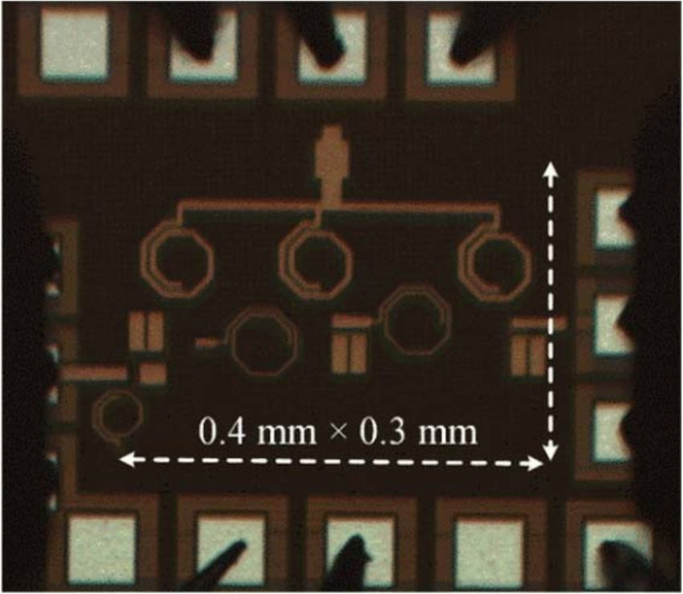
Fig. 17. Die micro graph of LNA ©[Reference Luo, He, Wang, Chang, Huang and Yu105]
A 16 cavity-backed slot antenna was designed on the back case of mobile. On left and right sides, two element phased arrays were built i.e on left and right sides of mobile casing for beam steering at broadside. The size of the antenna and Rogers 5880 substrate were 5.8 × 1.5 mm2. The thickness of substrate was 0.254 mm. The gain in the frequency band of 27.5–30 GHz was 6.9 dBi, and isolation level was more than 17.0 dB across the band of interest [Reference Yu, Yang, Sim and Yang106].
The 2 × 2 and 3 × 3 series-fed patch antennas were designed with connected patches to have high-impedance microstrip lines. Two types of designs were implemented, the first design with one phase shifter resulted in good radiation and impedance characteristics, while the second design threw light upon ways to decrease number of ports. The Rogers RT/Duroid 5880 of thickness 0.25 mm was used to design 27.61–28.43 GHz frequency band antenna, having gain of 7.73 dB, efficiency of 88.0%, and isolation level of >29.0 dB. The designed antenna resonates at 28.0 GHz frequency. The design is shown in Fig. 18 [Reference Khalily, Rahman and Kamarudin107].

Fig. 18. 2 × 2 and 3 × 3 series-fed array antennas ©[Reference Khalily, Rahman and Kamarudin107]
A 28.0 GHz switched five beam antenna consisted of rectangular waveguide and reconfigurable semiconductor circuit (RSC) was designed with slots which could be opened/closed with the help of switch pin to achieve desired configuration. The RSC was attached with WR28 waveguide to compose reconfigurable radiating structures (RRSs). These RRS structures formed 3 beams which were directed towards 0°, 30°, and 45°. The gain of each beam was similar because of the opening ofa different number of slots in odd number i.e 3, 5, 9 which produced beams in 0°, 30°, and 45°, respectively. High-current operational amplifiers were used to control antenna's aperture. In the frequency band of 27.9–28.5 GHz, antenna yielded gain of >6.0 dBi [Reference Yashchyshyn, Derzakowski, Bogdan, Godziszewski, Nyzovets, Kim and Park108].
A 1 × 4 antenna array was designed to resonate at 28.0 GHz and covered a band of 22.0–35.0 GHz, uses a U-shaped thin lens designed by phase shifting filter. This lens was placed at a distance of 5.0 mm from the antenna array, whose dimension was 4.1 × 30.6 × 8.3 mm3. A single element in array consisted of 1 driven element and 2 parasitic directors. The driven element contained one top and bottom patch plates separated by FR-4 substrate. The top patch plate was connected to feedline whereas bottom one to ground. Similarly, directors have top and bottom plates, connected through shorting vias. The gain was >3.8 dB and efficiency was 43.0%. The size ofthe antenna was 24.7 × 20.8 × 0.8 mm3 on Rogers 6010 substrate having thickness of 0.25 mm [Reference Kim, Ko, Lee and Oh109].
A radial line slot array antenna (RSA) designed to cover frequency band of 27.0–29.0 GHz (resonating at 28.0 GHz) consisted of 2 parallel plates. The upper plate contained radiated slot patterns, while lower plate acted as a ground. The patterns were cut in circular dimension on top of the board and the air was filled between ground and RT Duroid 5880 substrate. The gain was 23.3 dB and efficiency was 96.0% at resonate frequency. The size of the antenna was 78.0 cm2 on RT Duroid 5880 substrate [Reference Maina, Rahman and Khalily110].
To reduce mutual coupling, DGS was applied which included 12 unit cells arranged in a special manner, below the feeding line. Each unit cell contained two opposed C-shaped slot configurations used for concentrating magnetic and electric fields. Thus, a 4 × 4 microstrip patch array antenna was designed having three radial patches with tapering towards outer end. In the frequency band of 28.0–38.0 GHz, gain was more than 17.61 dB and efficiency was more than 92.2%, respectively. The size of Rogers Duroid RT 5880 substrate was 50.0 × 50.0 × 0.508 mm3. The design is shown in Fig. 19 [Reference Mahmoud and Montaser111].

Fig. 19. 12 unit cell array antenna (a) Front view (b) Back view ©[Reference Mahmoud and Montaser111]
An array was designed on Franklin array concept in order to obtain multiple frequency bands instead of single one. The non-radiating stubs turned into folded-dipole antennas and radiating patches shared a phase shift of 180°. Therefore, the antenna consisted of rectangular patch and a stub, both radiating at different frequencies. The gain was achieved as 13.5 dBi with 70.0% efficiency in the 37.0–39.0 GHz frequency band. The thickness of Rogers RT/Duroid substrate was 0.8 mm. The design is shown in Fig. 20 [Reference Jilani and Alomainy112].

Fig. 20. Franklin array concept-based antenna ©[Reference Jilani and Alomainy112]
CP achieves good 3D beam-steering characteristics, and this was showed with the help of an antenna having 12 dual-band CP antenna elements, which formed linear array in the edges of mobile phone. In this way, reflection coefficient of less than − 15.0 dB, more than 7.68 dB gain, more than 15.0 dB isolation, more than 64.75% efficiency, and <3.0 dB AR values were achieved in the 28.0–38.0 GHz frequency band. The size of 0.8 mm thick N9000 PTFE substrates were 110.0 × 55.0 × 1.6 mm3 [Reference Mahmoud and Montaser113].
An antenna was placed in front of a wideband lens to increase the gain. The four substrates namely RT 3003, RT 6002, and RT 5870 were used to form multi-layer antenna. The height of substrates were 0.765, 0.5, and 0.254 mm, respectively. The antenna was excited by a tilted slot having a CP ME-dipole. The lens consisted of three layers of mu-near zero (MNZ) unit cells and each layer consisted of 3 × 4 dual-polarized low index meta-material unit cells. In the frequency range of 31.0− 35.0 GHz, the gain was >10.0 dBi, while efficiency was >94.0% [Reference Dadgarpour, Sorkherizi and Kishk114].
A 1 × 4 array antenna with tapered line feeding technique was designed to achieve 12.0 dB for mobile applications. The distance of 4.0 mm was present between the adjacent elements. Thus, for 5G communication, microstrip patch antenna was used to resonant at 38.0 and 54.0 GHz frequencies with 1.94 and 2.0 GHz bandwidths in each band respectively. The size of the antenna and Rogers RT 5880 substrate were 6.0 × 6.25 × 0.578 mm3 and 6.0 × 6.25 × 0.508 mm3, respectively. The gains of 6.9 and 7.4 dBi were achieved for 38.0 and 54.0 GHz frequencies [Reference Peristerianos, Theopoulos, Koutinos, Kaifas and Siakavara115].
To enhance gain in 5G mobile antenna a bow-tie parasitic cell was developed, which includes several bow-tie directors and parasitic patches. Bow-tie directors were based on quasi-yagi principle. The patches enhanced antenna gain by increasing transverse radiation aperture of antenna. Rogers 5880 substrate of thickness 0.508 mm was used to design the antenna for 40.0–50.0 GHz frequency band, having gain between 7.3 and 12.5 dBi [Reference Chu, Li and Ye116].
A 2 × 2 sub-array antenna was formed using complementary sources, having two dipoles on the opposite sides of slot and surrounded by a cavity. Using the above design, 4 × 4 and 8 × 8 large antennas have been developed. The frequency band covered a range of 50.0–74.0 GHz i.e. for 4 × 4 array it is 57.0–71.0 GHz and for 8 × 8 it is 56.1–70.6 GHz. Also for 4 × 4 array, gain and efficiency were 21.5 dBi and 90.0%, respectively, and for 8 × 8 array, it is 26.7 dBi and 80.0%, respectively. The overall gain of antenna was 8.7 dBi. The antenna dimensions of 44.4 × 14.4 × 2.5 mm3 for 4 × 4 array and 28.8 × 28.8 × 2.5 mm3 for 8 × 8 array were utilized on Rogers 5880 substrate having 0.787 mm thickness. The design is shown in Fig. 21[Reference Zhu, Ng, Chou and Luk117].

Fig. 21. Antenna arrays (a) 4 × 4 (b) 8 × 8 ©[Reference Zhu, Ng, Chou and Luk117]
For operation in short range having high-data rate under 60.0 GHz wireless personnel area network (WPAN) systems, an antenna was designed having edge-coupled parasitic patch structure and a rotational feeding network. The designed antenna was used to obtain broad impedance bandwidth via dual resonance. The first resonance occurred due to circular patch antenna at 59.0 GHz, while second resonant was due to parasitic patch radiator occurred at 64.5 GHz. The gain of >12.0 dBic was obtained in the frequency range of 53.3–66.5 GHz. Taconic RF-30 substrate having 18.0 × 18.0 × 0.254 mm3 dimension was used to design the antenna. The design is shown in Fig. 22 [Reference Lee and Yoon118].

Fig. 22. 60.0 GHz WPAN antenna array ©[Reference Lee and Yoon118]
An antenna was designed having a combination of fabry-perot cavity (FPC) and printed ridge gap waveguide techniques to improve the radiation performances. By placing dual-layer partially reflective surface (PRS) above a slot antenna, FPC was formed. This square slot controls the bandwidth and also adds degree of freedom. To feed the antenna, PRGW technology was used to excite the rectangular slot antenna on the Rogers RT 5880 material. The circular patches connected to ground plane acted as EBG and were printed on Rogers 3003 material of thickness 0.5 mm. Thus a dual-layer unit cell made of Rogers RT 5880 material of thickness 0.254 mm was designed to construct PRS to operate at 60.0 GHz. The efficiency of better than 90.0% and gain of 16.8 dB were achieved in the frequency range of 55.4–66.6 GHz. The antenna dimension was 14.8 × 18 mm2 [Reference Attia, Abdelghani and Denidni119].
A meta-surface sandwiched between two DRAs was arranged in H-plane to increase isolation. This meta-surface was constructed of split ring resonator (SRR) which functions as band-stop filter over 60.0 GHz frequency range. The conductive elements of SRR acted as conductive material and the gap in ring as capacitive material. The SRR was fabricated on top and bottom of RT 5880 material having thickness of 0.254 mm, while DR and rectangular slot on the upper side of substrate. Lower substrate fabricated with RT 6010 having thickness 0.254 mm consisted of feedlines to excite DRA through rectangular slot cut out of upper substrate. Thus 1 × 2 DRAs having 1 × 7 SRR array was designed to cover 56.6–64.8 GHz frequency range yielding 7.9 dBi gain and 91.0% efficiency. By loading DRA with 1 × 7 array of unit cells, the obtained isolation was 46.5 dB [Reference Dadgarpour, Zarghooni, Virdee, Denidni and Kishk120].
The three antenna arrays, each having 16 patch elements were fabricated on top of RT/Duroid 5880 substrate material having height of 0.127 mm. Each of them were placed parallely in 4 rows and 4 columns. On the bottom layer, DC lines for switch control were placed where the ground plane was also present. The achieved gain by first, second, and third arrays were 18.7, 18.6, and 18.8 dB, respectively . The frequency band covered a range of 57.0–63.0 GHz. The size of the antenna was 31.0 × 46.4 mm2. The design is shown in Fig. 23 [Reference Semkin, Ferrero, Bisognin, Laurinaho, Luxey, Devillers and Raisanen121].

Fig. 23. Array antenna (a)Planar prototype (b) Convex prototype ©[Reference Semkin, Ferrero, Bisognin, Laurinaho, Luxey, Devillers and Raisanen121]
Multi-sin-shaped corrugated antipodal fermi-tapered slot antenna (MSC-AFTSA) array was designed in which multi-corrugated patterns were implemented. The antenna consisted of grooved spherical lens (GS-lens). The three element wide scan profile AFTSA was fed to the spherical lens which orientated a wide angular coverage for transmission and receiver. The MSC was used to increase the optimization process. Together, they decreased side-lobes, enhanced radiation characteristics and impedance matching. The size of the antenna was 44.2 × 51.6 × 25.4 mm3 on RO 4003 substrate. The thickness of substrate was 20.0 mm. The gain and efficiency were 20.0 dB and 83.0%, respectively in the frequency band of 57.0–64.0 GHz [Reference Briqech, Sebak and Denidni122].
A 4 × 4 multi-beam antenna array, generating 16 beams was designed using aperture-coupled ME-dipole antennas. The stacking of five Rogers 5880 substrates of thickness 0.787 were used, where vertical inter-connections were realized using substrate 1 to 3 while horizontal interconnection through 4 and 5 substrates. The gain yielded between 10.0 and 14.7 dBi and efficiency between 35.0 and 40.0% in the frequency range of 57.0–64.0 GHz. Antenna's total dimension was 5.0 mm × 5.0 mm [Reference Li, Wang and Luk123].
Similarly, two planar antennas were designed for 60.0 GHz spectrum, where, each one consisted of a 2 × 2 array covering 2 channels. The first antenna achieved maximum gain in point-to-point link over maximum distance of 10.0 m, while the other one was used in point-to-multipoint applications to achieve maximum beam-width. The range of frequency band was 57.0–65.0 GHz. RT Duroid 5880 substrate was used with 10.0 mil thickness. The size of the first antenna with 13.2 dBi gain was 0.25 cm2, and that of the second one with 10.3 dBi was 0.16 cm2. The design is shown in Fig. 24 [Reference Biglarbegian, Fakharzadeh, Busuioc, Ahmadi and Naeini124].

Fig. 24. 2 × 2 array antenna for 60.0 GHz spectrum ©[Reference Biglarbegian, Fakharzadeh, Busuioc, Ahmadi and Naeini124]
A CP antipodal curvedly tapered slot antenna (CP-ACTSA) array was designed, which was fed by substrate-integrated waveguide. Rogers 6002 substrate having thickness 0.762 mm was filled with two different rectangular waveguides. The waveguide having wider section consisted of two symmetrical, antipodal and exponential tapered slots. This waveguide was fabricated by wire cutting electrical discharge machine. The slots further consisted of two curves. Thus, the CP antenna array was able to cover 5G upper E-band i.e from 81.0 to 86.0 GHz and 5G upper W-band i.e from 92.0 to 95.0 GHz. The size of the antenna was 9.55 × 12.0 mm2, with 19.88 dBic gain and 80.6% efficiency [Reference Yao, Cheng, Wang, Yu and Chen125].
Beam steering techniques and transceiver
The beam steering is a challenge for 5G antennas. Most of the work is carried out on beam steering with 5G array antennas. Beam steerable is the process of controlling interference in terms of channeling far-field radiation pattern in a particular direction where high path loss, signal attenuation, and misalignment due to heavy air flow are prevalent. The beam steering is the ability of millimeter wave and an essential part of communication and Radar. In the past, most of the beam steering techniques were utilized, but at the expense of antenna only. The different techniques to steer the radiation pattern of an antenna are: Beamforming, Mechanical (based on MEMS switches), Reflectarray (Reflector and array), Integrated lens antenna (ILA), Switched beam antenna (antennas are arranged to cover the particular angle), Retrodirective antenna (to redirect radiation towards origin), Traveling wave antenna, Parasitic steering, and Metamaterial antenna-based [Reference Uchendu and Kelly126].
In a two array system, first array was fed with the currents in quadrature with the other array to obtain the desired far field radiation pattern. Thus, by controlling the amplitude of each array, beam steering is achieved [Reference Costas127]. In a design, electronically steerable beam was produced by altering the parasitic element and using simple switching and tracking circuitry. The same design utilized the active element, and the parasitic element was placed at a position between open and short circuits to reduce induced current. This in turn controls the radiation losses [Reference Thiel, O'Keefe and Lu128]. A combination of electrically and mechanically beam steering uses the monopole and parasitic elements to make frequency dependent far field radiation performance. An impedance matching network is utilized to feed the antenna and parasitic elements [Reference Katare, Biswas and Akhtar129].
The modern phase shifter monitors the phase difference between the closest radiator and microcontroller and then controls the phase shifter for the desired beam using miniaturized antenna arrays [Reference Kojima, Shiramatsu, Chiba, Ebisui and Kurihara130]. A design uses a combination of oscillators and phase locked loops (PLL) to steer the beam by switching array antenna using a single control voltage. The beam scanning range is the function of frequency of the PLL. The beam positioning error can be controlled, to produce sum and difference radiation patterns using double pole-double throw switch and difference amplifier. By the use of prescalers, ± 900 beam scanning extension can be achieved. The configuration of antenna array with coupled phase locked loop is given in Fig. 25 [Reference Yan and Chu131].

Fig. 25. Configuration of antenna array with coupled phase locked loop array ©[Reference Yan and Chu131]
The modified beam steering can combine the cassegrain antenna structure, where main reflector and sub-reflector are used. The sub-reflector due to light weight and rotational nature is able to steer beam, whereas, phase of the array is controlled by proper feeding. The design was utilized for satellite communication [Reference Jung, Shishlov and Park132].
At 28 GHz 2 × 3 and 2 × 4 arrays with single phase shifter on each port was utilized with unequal amplitude application. Hence, number of radiating elements were minimized. The approach produced better impedance matching, better radiation beam, and reduction in side/back lobe levels [Reference Nassar, Soliman, Ghoneim and Abuelenin133].
Along with the beam steering techniques, there is a beamforming technique also for the Massive MIMO technology for the next generation of 5G applications to reduce the intra- and inter-cell interference problems [Reference Ali, Ismail, Nordin and Abdulah134].
In an adaptive beam steering system, switched beam system is adapted to get desired radiation characteristics, and then beam steering is achieved by I and Q signal components. In this technique, phased local oscillator is used to adjust phase and weight of antenna element. Such method is used in steerable massive array to independently generate beams for 5G communication [Reference Hwang, Tsai and Hsiao135].
A CP switched beam array was designed using 90° branch line couplers, 45° phase shifters, and patched array [Reference Liu, Xiao, Guo, Bai and Wang136]. The CP provides line-of-sight communication and reduces multipath effects. The butler matrix with CP antenna array provides the desired rotation in beam within the scanning area in the range of 5.98–6.11 GHz with peak gain of 7.8 dB. The switched beam antenna with 4 × 4 butler matrix is given in Fig. 26 [Reference Liu, Xiao, Guo, Tang, Bai and Wang137].

Fig. 26. Switched beam array antenna using butler matrix ©[Reference Liu, Xiao, Guo, Tang, Bai and Wang137]
A 28 GHz CMOS transceiver was designed with 2 × 4 patch antenna array for 5G application. The design achieved good beam control arrangement and better RF performance parameters. The construction of the transceiver is explained in detailed here. The radio system consisting of 8-channel transceiver array is interfaced with digital front-end (DFE) to process baseband signals. The P-I-N diode switches are used since time division duplex (TDD) mode is used for operation. On the front end, 8-commercial 9-W power amplifiers (PA) along with 8 LNA are used that yields gain of 19 dB. Each pair of PA(LNA) is preceded by phase-shifter component giving an 11.25° phase resolution. Wilkinson power divider/combiner network is located between the RF front-end and the pre-amplifiers in 2 × 2 configuration. Operating frequency is regulated by serial peripheral interface (SPI) bus while phase shifters by shift registers via second SPI bus. A pumped gallium arsenide (GaAs) mixer containing integrated LO amplifier between intermediate frequency (IF) and final RF is used as up and down converter. Receiver path contains commercial logarithmic detector that works on IF frequency and is situated behind directional couplers. Finally, the antenna array is connected to the coupler for desired beam steering to achieve. The corresponding transceiver is given in Fig. 27[Reference Kim, Park, Oh, Song, Kim, Kim, Moon, Kim, Chang, Kim, Kang, Jung, Tak, Du, Suh and Ho138].

Fig. 27. Block diagram of transceiver at 28 GHz ©[Reference Kim, Park, Oh, Song, Kim, Kim, Moon, Kim, Chang, Kim, Kang, Jung, Tak, Du, Suh and Ho138]
THz technology
As our technology is getting advanced day-by-day and so are its uses, we are in need of such a set of frequencies which will fulfill all our requirements and demands, which was not earlier by lower frequencies. Tera-hertz (THz) technology will meet the growing demands in the field of medical, astronomical, sensing, defence, communication, etc. The one THz or 1012 Hz is a set of frequencies between infrared and microwave frequency bands. The reason of this growing demand of THz technology is because of its capability to penetrate high with low attenuation loss, non-ionizing nature, high-resolution imaging power, etc. The Thz frequency spectrum is aimed to work over the 10.0 Giga bits per second data rates and spectral efficiencies of more than 120.0 bits per second to avoid the unnecessary delays in critical situations like bomb detection, material testing, patient report/state trans-communication etc.
Thz frequency range (0.1–10.0) can be fulfilled by using photonic band-gap structures (PBG) as one of the options. Graphene was used as a substrate due to its ability to control surface waves. The drawback of graphene antennas was that they suffer deterioration of radiation efficiency, but overall it has very high electrical conductivity, directivity, and miniaturized structure.
Earlier to fabricate antenna, copper was used but as it suffered degradation in radiation efficiency and propagation loss, it was replaced by copper nanotube (CNT) and graphenes. The reason for opting CNT and graphene is because, CNT has high conductivity and kinetic inductance as compared with copper, and graphene is used now-a-days because of its ability to support slow plasmonic rays at THz frequency. Therefore, graphene is preferred mostly upon CNT and copper. In THz frequency, copper's skin depth and conductivity decreases as increase in frequency.
Graphene was discovered by Novoselov et al. in 2004, is a 2D mono layer of sp 2-bonded carbon atoms, having 1.42 mm spacing betweentwo carbon atoms and 0.335 mm inter-planar spacing between two graphene sheets. The structure of the graphene is a honeycomb type lattice structure. It is a zero-overlap semiconductor having high electrical conductivity. Narrow strip of graphene sheet called GNR is of two kinds, armchair and zig-zag.
Armchair-shaped edges behave both either metallic or semiconductor while zig-zag behave only metallic. Due to its property of propagating waves of surface plasmon polariton, it is laid in infinite thin sheet having complex surface conductivity. This conductivity can be both intraband and interband. However, intraband dominates over interband in low THz frequency range. The CNT was discovered by Sumio Iijima in 1991, is nothing but rolled form of graphene sheets. They can be either single-walled or multi-walled. Single-walled can be zigzag which is an insulator, armchair, a conductor and chiral, semi-conductor. Power dissipation is low in CNT materials, leading to high antenna efficiency. The CNT also supports slow-wave propagation, enabling high miniaturization. Graphene is a planar structure while CNT and copper dipoles are cylindrical structures. At one THz frequency, length of graphene dipole antenna is 68.0 μm, copper dipole antenna's length is 139.0 μm and CNT antenna's length is 99.0 μm and directivities are 3.27, 2.26, and 3.02 dBi, respectively. The design is shown in Fig. 28 [Reference Dash and Patnaik139].

Fig. 28. Modeled THz copper, CNT and graphene dipoles of lengths L1, L2, and L3, respectively ©[Reference Dash and Patnaik139]
A design with graphene was used as a substrate to support highly-confined surface waves of lower wavelength. In a design, three patch antennas on three substrate materials i.e silica-oxide, epsilon-near-zero (ENZ) medium, and air were used. The dimensions of these tree substrate materials were, 11.2 × 5.6 mm2, 24.0 × 12.0 mm2, and 48.7 × 24.35 mm2, respectively. The efficiency was 16.6% in the frequency band of 1.0–2.0 THz. The design is shown in Fig. 29 [Reference Amanatiadis, Karamanos and Kantartzis140].

Fig. 29. Graphene plasmonic antenna ©[Reference Amanatiadis, Karamanos and Kantartzis140]
Similarly, the polyimide substrate with rectangular patch antenna and with circular cut from both broad sides was designed with photonic band gap (PBG) structures to resonate in 0.615–0.651 THz frequency band on 800.0 × 600.0 × 191.29μm3 polyimide substrate. The rectangular patch was cut in a curvature of radius 75.0 μm from both the sides. This cut in radius reduced the size of the antenna and the PBG structure resulted in high peak gain and efficiency. The gain and efficiency of the designed antenna were 7.934 dB and 85.93% respectively. The design is shown in figure 30. The dimensions of rectangular patch antenna were calculated by equations (33) and (34) [Reference Kushwaha, Karuppanan and Malviya141]:
 $$W_{\,p}={2M+1 \over \varepsilon_{r}}\, \ast\, {\lambda _{o} \over 2}, $$
 $$L_{\,p}={2N+1 \over \sqrt{\varepsilon_{eff}}}\, \ast \,\left( {\lambda \over 2} \right)-2 \;\ast\; \Delta L, $$
where W p and L p were the width and length of patch respectively, M and N were non-negative integers, λo and λ were free space and operating wavelengths respectively, ΔL was patch length extension due to fringing field effect. The width of feed, W f was calculated by equation (35):
 $$W_{\,f}={7.475h \over {\rm exp}(x)}-1.25t, $$
where t is patch thickness, and x is formulated by equation (36):
 $$x=Z_{o}{\sqrt{\varepsilon_{r}+1} \over 87}. $$
Fig. 30. THz antenna with PBG ©[Reference Kushwaha, Karuppanan and Malviya141]
The dimensions of substrate and ground were calculated by the formulas, having W s, W g, L s and L g as width and length of substrate and patch, respectively, by equations (37) and (38) as:
 $$W_{s}=W_{g}=W_{\,p}+2 \,\ast\, L_{\,f}, $$
 $$L_{s}=L_{g}=L_{\,p}+2 \;\ast\; L_{\,f}. $$
To use antennas in THz applications, graphene plasmonic antennas are attracting researchers and industrialists. Earlier, THz antennas were using copper, graphene, and carbon nanotubes, but since they did not meet all the requirements of THz applications, surface plasmon polariton (SPP) was used so that applications and requirements of THz range can be fulfilled. The silicon-oxide material having dimension of 80.0 × 15.0 × 1.0 mm3 was used as substrate. The frequency range lied between 0.1 and 10.0 THz [Reference Dash and Patnaik142].
4G and 5G combined antennas
Some of the designs are using the 4G and 5G combinations to accommodate both the generations of antennas. Few of the available designs are included in literature.
To cover bands of both 4G and 5G, a MIMO and connected antenna array (CAA) was combined. The CAA etched on ground plane was excited using slot and also uses 2 × 1 power divider/combiner arms. The lower bands of 4G antennas were covered using 4-element MIMO monopole antenna system while CAA slot covered 5G band. The gain and efficiency achieved on lower side were 5.0 dBi and 80.0%, respectively, while upper side achieved 9.65 dBi gain and 75.0% efficiency. The size of the antenna was 14.5 × 11.0 mm2, with isolation of >13.0 dB, and ECC of <0.5 were achieved with this design. The size of substrate was 115.0 × 65.0 × 0.76 mm3. The frequency bands covered 4G was from 1843.0 to 3305.0 MHz, while that of 5G was between 3500.0 and 3740.0 MHz. The design is shown in figure 31 [Reference Ikram, Sharawi and Shamim143].

Fig. 31. CAA MIMO antenna array ©[Reference Ikram, Sharawi and Shamim143]
A 4G/5G MIMO antenna system was made by integrating 2-element slots for 4G and 2-element MIMO-based connected array for 5G band. On the periphery of ground plane, two rectangular loops are etched. The thin loops on top and bottom act as 4G MIMO and parts of sides act as 5G arrays. The thickness of RO 4350 substrate material was 0.76 mm. The dimension of single antenna was 100.0 × 60.0 × 0.76 mm3. For 4G, gain was 2.22 dBi, and for 5G gain was 8.0 dBi. Two resonant frequencies at 2.45 and 17.3 GHz were obtained with efficiencies as 27.0 and 80.0%, respectively. By implementing four narrow loops, isolation can be enhanced greatly in the band of 16.50–17.80 GHz. The value of ECC was <0.5 in the band. The design is shown in figure 32 [Reference Sharawi, Ikram and Shamim144].

Fig. 32. Integrated design with isolation enhancement structure ©[Reference Sharawi, Ikram and Shamim144]
The three-port MIMO DRA having three mutually decoupled modes was achieved by exciting two modes out of three and then overlapping the third perpendicular to their field magnitudes. The gain of 8.1, 7.4, and 7.5 dB was attained in the 8.6–10.2 GHz frequency range, having 720.0 MHz bandwidth. The antenna consisted of two parts, i.e rectangular DRA and feeding system. Rectangular DRA was fabricated on Rogers RT 6010 and feeding system which consisted of two microstrip lines having five identical apertures etched on ground plane. The feeding system placed on lower substrate was made of Rogers RT 5880 material. Overall dimensions of antenna and substrate were 56.6 × 56.6 × 14.09 mm3 and 31.5 × 17.8 × 13.3 mm3, respectively. In the desired bandwidth, ECC was <0.002 and isolation was 20.0 dB. The design is shown in figure 33 [Reference Abdalrazik, Hameed and Rahman145].

Fig. 33. Multi-mode MIMO DRA antenna ©[Reference Abdalrazik, Hameed and Rahman145]
Finally, the 5G antennas have been summarized and compared in tables 2 and 3 on the basis of the frequencies used for 5G for single element/array/MIMO antenna. The other parameters compared in these tables are no. of radiating elements, size of the designed antenna, gain, efficiency, and isolation. Most of them are arrays and MIMO antennas. The designers/researchers used various bands for the 5G technology and ultimately, the goal is to make them compact, high gain for single and multi-element/port, and highly isolated in the case of multi-element/port antennas for different applications.
Table 2. Comparison of antennas having 28.0 GHz frequency range

Table 3. Comparison of antennas having 60.0 GHz frequency range

Conclusion
The 5G wireless network will specify the growth beyond mobile internet to massive IOT in the upcoming years. Main highlights compared with 4G/4G LTE is that besides data speed requirements, IOT and communication mechanisms will require new types of improved performances. Unlike IOT current services, 5G networks will be designed to bring the level of performance needed for massive IOT.
Different types of structures were investigated like PEG, PSG, SIW, corrugated structures, multiple notch, RRS, and PBG. Along with these structures, various kinds of antennas and arrays like patch/dipole/folded antennas, power divider arms-based arrays, combined antenna arrays, MIMO, etc on numerous kinds of substrates like FR-4, Taconic TLY-5, Rogers TMM4, Rogers 4003, Rogers 5800, etc have been studied and presented in this paper. The effects of stubs, slots, slits, parasitic element directors, baluns, CPW-fed with T-shaped element, etc have been presented with their impacts on the parameters of antenna. Thus, It has been observed that most of the structures provided higher than 80.0% efficiency, >10.0 dBi gain, and ECC of <0.01. The 5G can be considered as a boon to the market with its compact size and higher gain, high data rate, and battery life etc. The effect of beam steering with the transceiver showed the desired direction of radiation. Definitely, the higher capacity and accommodation of growing population can be done with the 5G and THz applications. Apart from 5G antennas some of the available THz antennas with different dielectric substrates have been discussed.
Author ORCIDs
Leeladhar Malviya, 0000-0002-7342-4766
 Parul Gupta is currently pursuing her ME in Electronics and Telecommunication Engineering from Shri G. S. Institute of Technology and Science, Indore (MP), India, in session 2017-19, and procured her BE in Electronics and Communication, from Indore Institute of Science and Technology, Indore (MP), India, in 2017. Her current research interests include compact multiple-input-multiple-output (MIMO) antennas for high data rate communications for 5G and planar microstrip antennas.
 Leeladhar Malviya received his Ph.D. from IIT Roorkee, India in 2017. He received his ME in Electronics and Telecommunication Engineering from Shri G. S. Institute of Technology and Science, Indore (MP), India, in 2008, and BE in Electronics and Communication, from the Govt. Engineering College, Ujjain (MP), India, in 1998. Since 2001, he has been with Shri G. S. Institute of Technology and Science, Indore (MP), India, and serving as an Associate Professor. His current research interests include compact multiple-input-multiple-output (MIMO) antennas for high data rate communications for 4G, 5G, and THz planar microstrip antennas, fractal antennas, and metamaterial antennas for communication. He is a Member of IEEE, Institution of Electronics and Telecommunications Engineers (IETE, India) Institution of Engineers (IE, India), and Indian Society for Technical Education (ISTE).
 Prof. S. V. Charhate is currently working in Shri G. S. Institute of Technology and Science since 1985. She received her ME in Computer Science Engineering from DAVV University, Indore (MP), India, in 1991, and BE in Electronics and Communication, from the Pune University, India, in 1981. She is a Member of Institution of Engineers (IE, India).


