


Introduction
Driven by the demand for the lowest bill of materials, the level of system integration is ever increasing. The advances in silicon-based semiconductor processes and packaging technologies enable the realization of the highly integrated system on chip (SoC) and system in package (SiP) solutions for millimeter-wave (mm-wave) applications. Silicon-based technologies offer high integration capability that can enable the realization of low-cost mm-wave radar sensors. Furthermore, silicon-based processes have been proven to have competitive performance compared with the III–V and SiGe heterojunction bipolar transistor (HBT) technologies [Reference Voinigescu, Dickson, Gordon, Lee, Yao, Mangan, Tang and Yau1].
Complementary metal–oxide–semiconductor (CMOS) is particularly attractive due to the highest potential for high-level integration of RF, analog, digital, and power circuitry. The recent advances in CMOS technology nodes have enabled it to become an inexpensive alternative for the realization of millimeter-wave integrated circuits. Metal-oxide-semiconductor (MOS) transistors achieve transit frequencies (f T) and maximum oscillation frequencies (f max) in excess of several hundreds of gigahertz. Several advanced nano-scale CMOS nodes even surpass f T and f max values achieved by SiGe HBT technologies [Reference Voinigescu2]. However, it is still a challenge to achieve the noise performance, linearity, output power, and temperature robustness, required for mm-wave radar sensor products in bulk CMOS technologies. Hence, the commercial solutions for integrated radar chipsets at mm-wave frequencies are still realized mainly in SiGe bipolar technologies due to the outstanding RF performance of the HBT transistor [Reference Knapp, Treml, Schinko, Kolmhofer, Matzinger, Strasser, Lachner, Maurer and Minichshofer3–Reference Forstner, Knapp, Jager, Kolmhofer, Platz, Starzer, Treml, Schinko, Birschkus, Bock, Aufinger, Lachner, Meister, Schafer, Lukashevich, Boguth, Fischer, Reininger, Maurer, Minichshofer and Steinbuch5].
Nevertheless, an interesting trend can be observed is that a number of new radar chipset products emerging on the market realized in advanced CMOS nodes is rapidly increasing. This is mainly driven by the need to integrate complex digital and mixed-signal blocks, such as a microcontroller, memory, serial peripheral interface (SPI), FPGA, ADC, and a digital phase-locked loop (PLL) on the same SoC. Use of newest CMOS nodes for this purpose is absolutely inevitable, thus driving the research efforts on mm-wave front-ends in advanced nano-scale CMOS technologies. However, it should be mentioned that due to high mask costs the use of advanced nano-scale CMOS nodes makes sense for product realization only if sufficiently high production volumes can be achieved. Potential commercial applications that can achieve such mass volume of units are chipsets integrated in portable mobile devices (e.g. LTE and 5G cellular transceivers or radar-based sensors for smartphones, tablets, and smart watches), wireless consumer products and chipsets for Internet of Things.
Unfortunately, standard bulk CMOS technologies suffer several disadvantages compared with SiGe HBT processes, such as a higher flicker noise, lower supply and lower breakdown voltages, lower current efficiency (ratio of achievable transconductance to DC current), thinner lower metal layers, and higher losses of passive components due to closer proximity to a lossy silicon substrate. This has several negative effects particularly for the realization of voltage-controlled oscillators (VCOs). Firstly, the flicker noise is modulated onto the oscillation as sidebands and contributes to the phase noise close to the carrier. Particularly, in radar systems operating with very low intermediate frequencies (IF) the absolute value of phase noise is dominated by the flicker noise. MOS transistor exhibits very high corner frequencies of several megahertz as opposed to few kilohertz exhibited by a bipolar transistor [Reference Issakov, Siprak, Tiebout, Thiede, Simburger and Maurer6]. This results in a worse phase noise performance achievable by CMOS VCO compared with a SiGe HBT VCO.
Secondly, based on the classical phase noise model of Leeson [Reference Leeson7], the phase noise can be reduced by increasing the voltage swing. However, this is possible up to a certain point, at which the voltage limited operation regime is reached. In this regime, the differential amplitude in the tank achieves the supply rails. Hence, it is not further possible to increase the amplitude to reduce the phase noise. However, the supply voltage in the advanced CMOS nodes is being systematically reduced due to MOS device scaling.
Additionally, to reduce the phase noise, the quality factor of the tank needs to be as high as possible [Reference Tiebout8]. However, the achievable quality factor is limited both by inductor and varactor at mm-wave frequencies. Due to thin lower metal layers, even if the inductors are realized in the thick top layers, if available, they are still too close to the conductive substrate. Thus, the maximum achievable quality factor of inductors is deteriorated due to the proximity to the lossy silicon substrate. Finally, the quality factor of varactor at the mm-wave frequencies is limited, reducing the overall quality factor of the tank. These drawbacks directly limit the lowest achievable phase noise of CMOS VCO. One needs to overcome the aforementioned limitations by means of circuit level techniques.
In most RF and millimeter-wave systems, the absolute value of phase noise is one of the most important specified parameters imposed during the design of a VCO. It needs to be as low as possible to achieve best possible target discrimination. Furthermore, VCO with an ultra-wide frequency tuning range (FTR) is advantageous in frequency-modulated-continuous-wave (FMCW) radar applications to achieve a high range resolution. Multi-gigahertz FTR requires the use of very large varactors, which deteriorates the phase noise of a VCO. Hence, there is a trade-off between phase noise and FTR [Reference Tiebout8].
There are numerous works in the literature reporting CMOS VCOs at RF and mm-wave frequencies. The first target of every LC VCO design is the optimization of the LC tank for lowest phase noise and wide tuning range [Reference Ahmadi-Mehr, Tohidian and Staszewski9,Reference Tiebout10]. Most of the works in the literature focus on the optimization for highest figure of merit (FOM), rather than on achieving the lowest absolute phase noise. Hence, many works focus on power-efficient VCOs, e.g. class-C [Reference Fanori and Andreani11,Reference Kimura, Okada and Matsuzawa12], class-D [Reference Fanori and Andreani13], class-F [Reference Babaie and Staszewski14], and higher classes [Reference Babaie and Staszewski15]. Another target of VCO optimization is the reduction of phase noise degradation due to flicker noise. Thus, some research work is dedicated to the careful optimization of the bias network [Reference Tiebout10] or introducing a filter for the second harmonic (H2) [Reference Hegazi, Sjöland and Abidi16].
As discussed above, the minimum phase noise achievable by a single VCO core is ultimately bounded by technology limitations. Hence, even lower absolute phase noise levels, can be only achieved by coupling several VCO cores bilaterally [Reference Ahmadi-Mehr, Tohidian and Staszewski9,Reference Iotti, Mazzanti and Svelto17]. The phase noise is expected to reduce by  $10\cdot \log (N)$ for N cores [Reference Ahmadi-Mehr, Tohidian and Staszewski9]. However, to achieve the full expected phase noise improvement, the coupling network must be designed very carefully. This limits the maximal number of VCO cores N that can be coupled in practice.
Next, to address a need for VCO with a very wide frequency tuning range, also a large number of approaches is reported in the literature. However, most of the approaches use switches to extend the overall tunable frequency range by combining several narrower continuously tunable ranges (e.g. [Reference Ahmadi-Mehr, Tohidian and Staszewski9,Reference Yin and Luong18]). Also, the range can be extended by a combination of frequency tuning ranges corresponding to odd and even oscillation modes [Reference Jia, Chi, Kuang and Wang19]. Unfortunately, a combination of switched ranges is not easily applicable to FMCW radar, but rather to communication systems. Another option to extend FTR is to use a silicon-on-insulator (SOI) technology, if possible. SOI varactors exhibit lower parasitics, thus enabling a very wide tuning range with less phase noise deterioration [Reference Rimmelspacher, Weigel, Hagelauer and Issakov20].
This paper extends our conference publication [Reference Issakov, Rimmelspacher J Trotta, Tiebout, Hagelauer and Weigel21], in which we have presented a cross-coupled LC-VCO in a digital 40 nm bulk CMOS process without an RF option. Two cores are coupled magnetically via an LC-tank transformer to reduce the absolute phase noise value by 3 dB. Furthermore, to reduce the flicker noise contribution we have omitted the tail current source and added a H2 filter, which is also used as a balun to couple out a signal at the second harmonic for the push–push VCO operation. We optimize the tank for a wide frequency tuning range. The circuit achieves a low phase noise of −91.8 dBc/Hz at 1 MHz offset from a 62 GHz carrier and yet offers a wide tuning range of 25%. This circuit is suitable for application in FMCW radar systems requiring a very wide frequency tuning range and low phase noise.
This paper is structured as follows: Section “System considerations” describes radar system considerations. Next, Section “Design considerations” presents circuit design of the proposed VCO. Then, Section “Realization and measurement results” shows the measurement results. Finally, Section “Conclusion” compares the results to state of the art and concludes the paper.
System considerations
A typical FMCW radar system is shown in Fig. 1.

Fig. 1. Simplified FMCW radar system diagram.
A simple continuous wave (CW) radar system with a fixed transmit frequency allows determination of target velocity, but not the distance to the target. Therefore, varying the frequency of the local oscillator (LO) in time resolves this drawback, by evaluating the instantaneous frequency difference between the received signal f RX and the transmitted signal f TX at the mixer output. As shown in Fig. 1, the received frequency is a replica of the transmitted frequency shifted in time by a round-trip delay of the electromagnetic wave transmitted and echoed back  $\tau =({2R}/{c})$, where R is the range to target and c is the speed of light. Additionally, in case of a moving target, the received signal is further shifted by the Doppler effect
 $$f_d = \displaystyle{2v_r \over c} \cdot f_c,$$
where v r is the relative velocity of the target (due to radar or target movements) and f c is the transmitted frequency. Hence, the range to the target is evaluated from the traveling time of the wave and the the relative velocity of the target is determined from the Doppler shift of the returned signal. The system using a frequency varied periodically in a continuous sweep, e.g. using a triangular or sawtooth waveform, as shown in Fig. 1, is addressed as linear FMCW radar. As depicted in Fig. 1, the transmit signal varies between the minimum frequency f 0 and the maximum frequency  $f_0 + {\rm BW}$ with a period T, where BW is the bandwidth [Reference Issakov22]. A mixer produces a base-band signal at the instantaneous difference frequency between the transmit f TX and the receive f RX signals, referred to as the beat signal. For a sawtooth modulation, it is given by
 $$f_{IF} = f_R + f_d = \displaystyle{{{\rm BW}} \over T}\displaystyle{{2R} \over c} + f_c\displaystyle{{2v_r} \over c} \comma $$
where f c is the center frequency of the chirp signal [Reference Trotta, Wintermantel, Dixon, Moeller, Jammers, Hauck, Samulak, Dehlink, Shun-Meen, Li, Ghazinour, Yin, Pacheco, Reuter, Majied, Moline, Aaron, Trivedi, Morgan and John23]. For a triangular modulation waveform, the first range-related term is doubled (since the ramp occupies only half a period T/2) and the Doppler shift appears with an alternating sign for the rising and for falling slope of the transmit signal, also referred to as up-chirp and down-chirp.
The term resolution referred to the ability of a radar system to separate two closely spaced targets. In the example in Fig. 1 the transmitter illuminates two targets that are separated by a delta range  $ \Delta R $. From (2) in case of two targets the delta IF frequency is given by
 $$\Delta f_{IF} = \displaystyle{{{\rm BW}} \over T}\displaystyle{{2\Delta R} \over c} + f_c\displaystyle{{2\Delta v_r} \over c}.$$
To have an easier separation in beat frequency between two targets, we would like to increase  $\Delta f_{{IF}}$. This can be achieved by higher ramp slope (BW/T), which means either larger bandwidth BW or reducing the ramp time T.
Since the beat signal is a rectangular signal with a period 1/T for the sawtooth modulation, the corresponding spectrum is a sinc function and the first zero crossing occurs at 1/T. Thus, the smallest resolvable frequency is the reciprocal of the measurement time  $\Delta f=1/T$. Substituting this into (4) the minimal resolvable velocity is given by
 $$\Delta v_r = \displaystyle{c \over {2f_c}} \cdot \Delta f = \displaystyle{c \over {2f_c}} \cdot \displaystyle{1 \over T}.$$
Thus, for larger T and higher carrier frequency f c, higher velocity resolution can be achieved. However, from (3), the ramp should be short for better target separation. To resolve this, a fast Fourier transform (FFT) is applied over n chirps, thus velocity resolution corresponds to a time of nT [Reference Trotta, Wintermantel, Dixon, Moeller, Jammers, Hauck, Samulak, Dehlink, Shun-Meen, Li, Ghazinour, Yin, Pacheco, Reuter, Majied, Moline, Aaron, Trivedi, Morgan and John23].
Next, substituting  $\Delta f$ into (3) one obtains the range resolution
 $$\Delta R = \displaystyle{c \over {2{\rm BW}}}.$$
Hence, the range resolution can be increased only by using a larger bandwidth BW of the frequency sweep.
To address an impact of VCO phase noise in FMCW radar system, one can consider the qualitative description in Fig. 2. In the scenario of two targets, if the transmitted signal has a bad phase noise, the sideband of the reflected signal from a target with a larger reflection may completely cover the reflection of a target with smaller reflection (either farther apart or having a smaller radar cross-section). Hence, small targets may be hidden in the spectrum, making it impossible to detect them. As depicted in Fig. 2, there are two options that would help to detect the second target: (a) try to reduce the phase noise of the VCO as much as possible; (b) increase the separation of beat frequencies  $\Delta f_{{IF}}$, as already discussed above.

Fig. 2. Conceptual description of radar signals with a non-ideal VCO.
Additionally, as investigated in [Reference Trotta, Wintermantel, Dixon, Moeller, Jammers, Hauck, Samulak, Dehlink, Shun-Meen, Li, Ghazinour, Yin, Pacheco, Reuter, Majied, Moline, Aaron, Trivedi, Morgan and John23], noise density at the IF output is increased for higher phase noise of Tx signal. The phase noise of the free-running VCO in FMCW radar system is the phase noise of the transmitted signal. The Tx amplitude and phase noise smear the signal spectrum and raise the noise floor [Reference Trotta, Wintermantel, Dixon, Moeller, Jammers, Hauck, Samulak, Dehlink, Shun-Meen, Li, Ghazinour, Yin, Pacheco, Reuter, Majied, Moline, Aaron, Trivedi, Morgan and John23].
To sum up, a VCO should fulfill challenging requirements: provide a frequency tuning range as large as possible for high range resolution and larger beat frequency delta. The phase noise should be as low as possible. For velocity resolution, the operation frequency of the VCO should be as high as possible. Hence 60 GHz is advantageous for this purpose. The carrier frequency should be stable under every condition (load-pull, supply, and temperature) during transmission.
Design considerations
As has been explained in Section “Introduction”, there is a technological limit of phase noise that can be achieved by a single VCO core in CMOS. Coupling several VCO cores together allows breaking this limit. The conceptual diagram of the presented dual-core VCO is given in Fig. 3. The two cores are coupled magnetically via a transformer. Hence, they are locked and should oscillate in-phase. To avoid multi-mode oscillations, the two cores should be tightly coupled, requiring a high k-factor of the transformer. An alternative robust method to couple multiple VCO cores would be to use a resistive coupling [Reference Iotti, Mazzanti and Svelto17].

Fig. 3. Diagram of two coupled VCO cores.
Each core has its own resonant LC-tank. Hence, the high currents in the resonance are circulating in each VCO core locally. Ideally, in the presence of N coupled cores, the overall phase noise is N times lower than for a single core, or  $10\cdot \log (N)$ in dB [Reference Ahmadi-Mehr, Tohidian and Staszewski9]. However, also the power consumption is increased by the same factor. Hence, this would not improve the FOM of a VCO. We use here a dual-core VCO, since we are interested to achieve a low absolute phase noise value. Here we couple only two cores, since more cores would result in a larger area consumption, higher layout complexity, and would further increase the power consumption.
The detailed schematic diagram of the two coupled VCO cores is shown in Fig. 4. The VCO core circuit is based on the classical differential cross-coupled topology using NMOS transistors, similar to the one described in [Reference Craninckx and Steyaert24]. The VCO is realized in a push–push configuration, i.e. the LC-tank around the transformer T 1 is centered around 30 GHz, which is the fundamental oscillation frequency (denoted in schematics as first harmonic, H1). The fundamental differential output H1 is collected from the upper core, as shown in Fig. 4, while the second harmonic (H2) around 60 GHz is collected at the common source node of the transistors M 1 and M 2, denoted v tail, and amplified.
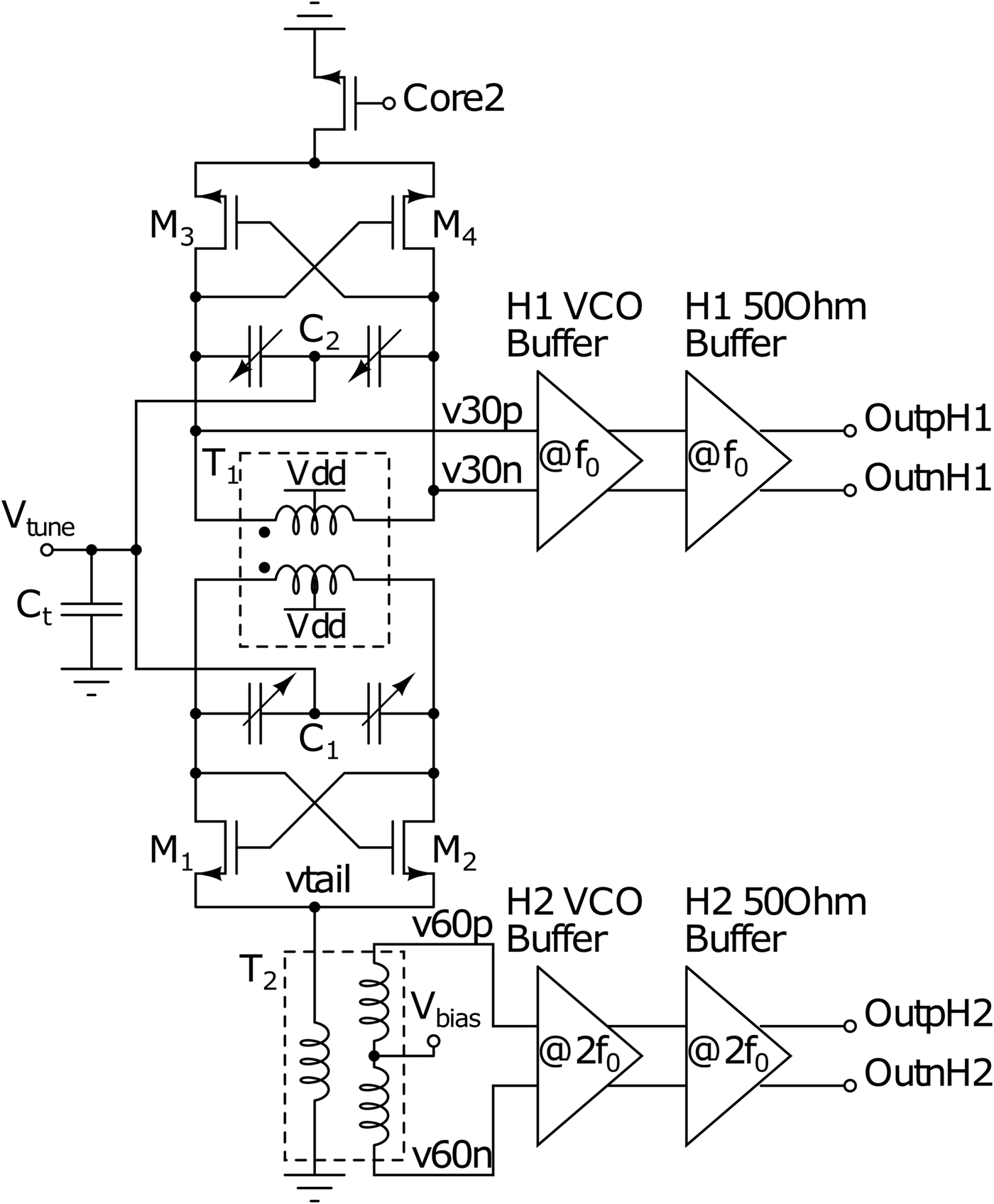
Fig. 4. Schematic diagram of the dual-core CMOS VCO.
The transistors  $M_1-M_4$ have a width of 60 μm and a minimal gate length of 40 nm allowed by technology. The width was chosen to provide on one hand a sufficient transconductance to generate a negative resistance for sustained oscillations, on the other hand, it was chosen as a trade-off between noise and tuning range. Larger devices are preferred for better switching, to reduce their noise contribution to phase noise at zero crossings. However, the device size was chosen not to too large to avoid parasitic capacitance which will reduce the FTR.
The design uses MOS varactors with an optimized maximum to minimum capacitance ratio, in order to maximize the tuning range. According to the model shown in [Reference Kinget25], the overall quality factor of the LC tank shall be maximized. The quality factor of the MOS varactor used in this design is still sufficiently high at 30 GHz and thus the overall tank quality factor is dominated by the inductor. However, the quality factor of varactors degrade significantly at mm-wave frequencies and VCO realized directly around 60 GHz would suffer from a low quality factor of varactors. Hence, this is an additional benefit to realize a VCO in the push–push configuration.
Transformer-based resonant tank optimization
The 3D model of the transformer T 1 used for the resonant tank and coupling of the two cores is shown in Fig. 5.

Fig. 5. Transformer 3D geometry used in EM simulation.
The transformer is formed by combining the tank inductor of the first and the second core, which are realized identically, and stacking them on top of each other. This way the 1:1 transformer, shown in Fig. 5, has been derived and optimized to couple the two cores. The cross-coupled pair and the varactors are attached between the terminals on the primary and secondary sides of the transformer, located opposite to each other. By this layout arrangement, we save chip area and realize a dual-core VCO at the expense of only a single passive component.
The transformer T 1 is realized in the two topmost metal layers by vertical stacking. The two cores are tightly coupled, resulting in robust locking of the two cores. By means of k-factor it is possible to define whether the two cores oscillate in-phase or out-of-phase. Both metal layers have a different metal thickness since RF option of two ultra-thick metal layers was not available here. However, at the fundamental oscillation frequency around 30 GHz the skin effect is dominant. Hence, most current flows in a narrow volume close to the conductor surface defined by the skin depth and the advantage of a thick top metal is reduced [Reference Issakov22]. This makes the asymmetry of the two cores less pronounced.
Figure 6 shows simulated inductance and quality factor of the primary and secondary side of the transformer.
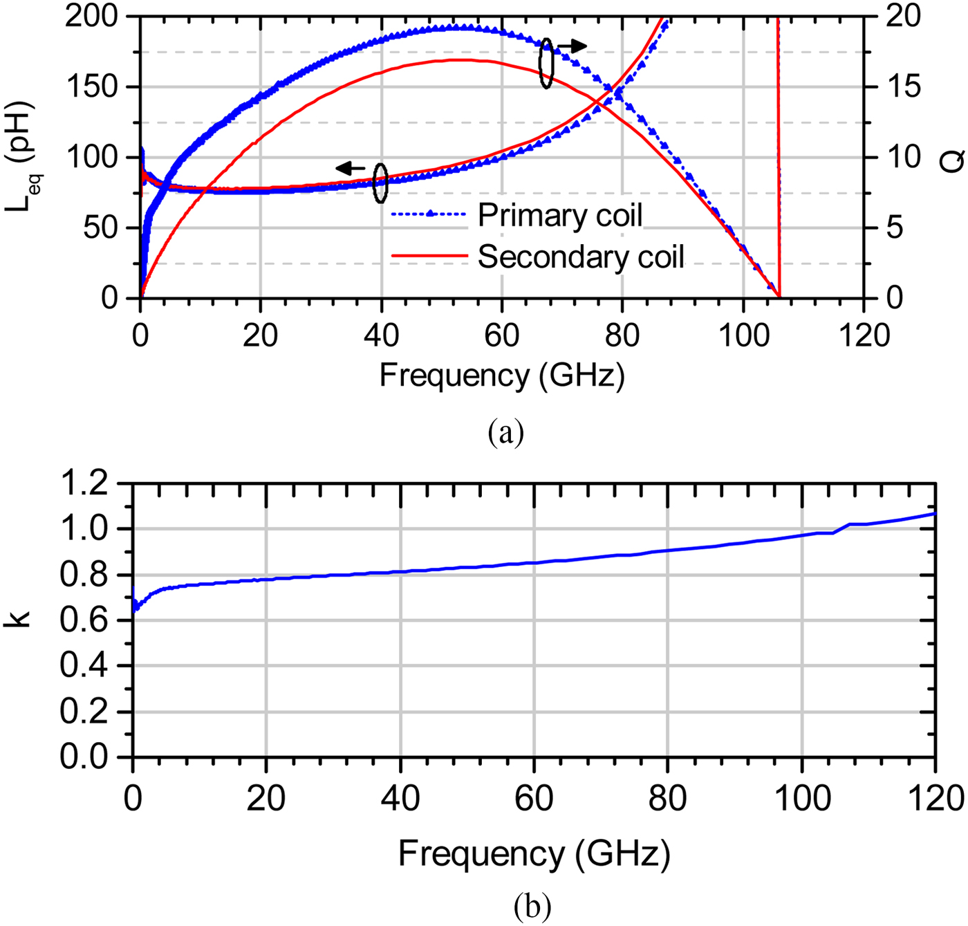
Fig. 6. Simulated characteristics of the transformer. (a) Inductance and quality factor. (b) k-factor.
As can be observed in Fig. 5, there is a slight asymmetry due to vertical stacking, since the secondary coil is closer to the substrate than the primary. Additionally, Fig. 6(b) shows that the transformer T 1 exhibits a high k-factor, about 0.8. For a good operation of a dual-core VCO k-factor of the transformers should be as close to 1 as possible. Additionally, the transformer exhibits a strong capacitive coupling between the coils. The high coupling is advantageous for sustaining a single mode oscillation, as both cores must be tightly coupled.
When employing transformed-based resonators, two modes of oscillation are possible [Reference Bevilacqua, Pavan, Sandner, Gerosa and Neviani26]. Even concurrent oscillations at incorrect frequencies may occur [Reference Goel and Hashemi27]. When several VCO cores are mutually coupled, the active devices of one core also “see” the input impedance of other cores through the resonator, hence multi-mode oscillations are possible. An equivalent circuit diagram representation of the transformer-coupled dual-core VCO is shown in Fig. 7(a). Negative resistance  $-1/G_m$ corresponds to the impedance looking into the drains of the cross-coupled pair on each side. Furthermore, Fig. 7(b) shows the input impedance looking input primary and secondary sides of the resonant tank. Looking into the tank we see a resonance at the fundamental frequency of 30 GHz. Additionally, there is a smaller resonance at around 90 GHz. However, the tank impedance is much lower at this frequency than at 30 GHz. Furthermore, G m of transistors at this frequency is very low, hence the oscillator loop gain is sufficiently small and oscillation cannot take place. Thus, a dominant mode will oscillate by design.

Fig. 7. Dual-core transformer-coupled oscillator circuit and input impedance. (a) Equivalent circuit. (b) Tank input impedance.
Despite the inherent transformer asymmetry due to the vertical stacking, the difference of electrical characteristics (inductance and quality factor) of the primary and secondary coils are minor. This can be also confirmed by comparing the input impedance looking into the primary and secondary side of the resonant tank, shown in Fig. 7(b). The difference in height of the resonances is negligible.
The transformer has been realized with a middle tap both on the primary and secondary side, as shown in Fig. 5. Both coils have been realized as a differential symmetrical inductor. The use of a differential coil makes it possible to increase the inductance per area, and thus we achieve higher L/C ratio. Additionally, since a differential inductor is used in a balanced configuration, part of the parasitics towards substrate is canceled out [Reference Tiebout8]. The middle tap is used for providing the power supply to the circuit, both at the primary and secondary sides for each VCO core. As a result of connecting the middle tap to the supply voltage in Fig. 4, a single VCO core can have a signal swing of up to twice the power supply voltage on each node. This is advantageous for minimization of the phase noise by means of signal maximization, as can be analyzed based on the LC-oscillator phase noise model of Leeson [Reference Leeson7]
 $${\rm {\cal L}}\left\{ {\Delta \omega } \right\} = 10\log \left( {F\displaystyle{{4kTR_p} \over {V_{{\rm sig}}^2 }}{\left( {\displaystyle{{\omega _0} \over {2Q\Delta \omega }}} \right)}^2} \right),$$
 where k is the Boltzmann constant, T is the absolute temperature, F is the noise factor,  $\omega _{0}$ is the center frequency,
  $\Delta \omega $ is the frequency offset, V sig is the steady-state output voltage amplitude, and R p is an equivalent parallel tank resistance. One can see in (6) that the voltage swing should be as large as possible. However, too large voltage swing may affect the long-term reliability of the circuit due to MOSFET degradation. Hence, swing is limited by the supply voltage.
Further, one can analyze from (6), the general requirement for design of VCOs, optimized for both low power and low phase noise, is the maximization of the tank quality factor [Reference Tiebout8]. Following the tank model described in [Reference Kinget25], the total quality factor of the tank is determined by the lowest quality factor component, since the quality factors of individual components are connected in parallel
 $$\displaystyle{1 \over {Q_T}} = \displaystyle{{Z_0} \over {R_p}} + \displaystyle{1 \over {Q_L}} + \displaystyle{1 \over {Q_C}},$$
where Z 0 is the tank impedance, R p is parallel losses, Q L and Q C are the quality factors of the inductor and capacitor, respectively. Therefore, the quality factor of the coils Q L needs to be maximized. It is achieved by increasing the width of the lines. The transformer traces were set to 12 μm, as wide as allowed by the technology.
Additionally, the resonant LC-tank comprising the transformer T 1 and varactors C 1, C 2 has been optimized for the lowest phase noise and reduced power consumption. The choice of the tank inductance poses a trade-off between power consumption, tuning range, chip area, and stability of oscillation [Reference Issakov, Wojnowski, Knoblinger, Fulde, Pressel and Sommer28]. It has been chosen following the procedure described in [Reference Ahmadi-Mehr, Tohidian and Staszewski9]. As can be observed in (6), to reduce the phase noise, the term  $R_{\rm p}/Q^2$ needs to be minimized. This corresponds roughly to minimizing the expression
  $L\omega /Q$ [Reference Ahmadi-Mehr, Tohidian and Staszewski9]. Hence, lower inductance value, having a highest quality factor is advantageous. However, as mentioned previously, there is a technological limitation on how low the inductance can be realized. Reducing the size of inductors results in lower inductance, but from a certain point, the quality factor drops since the resistive losses dominate. Hence, there is a “sweet-spot” point, beyond which increasing the value of inductance would degrade the phase noise, and reducing inductance would reduce the quality factor. As can be seen in Fig. 6, the inductance value of 75 pH is relatively small and still offers the high-quality factor of above 15 at the fundamental frequency of 30 GHz.
Transformer-based H2 extraction
As shown in Fig. 4, the H2 signal is collected at the common source node v tail by means of the transformer T 2. It also acts simultaneously as a balun and provides a balanced H2 signal at the secondary side, which is amplified by the subsequent buffer stages centered around 60 GHz. This technique is advantageous since the signal is picked up non-invasively and the H2 buffer does not load the operation of the VCO and does not degrade the phase noise performance. As shown in Fig. 8(a), the input impedance at the primary side of T 2 has a resonance around 60 GHz.

Fig. 8. Simulated waveforms at fundamental, H2 and tail nodes. (a) Input impedance looking into H2 filter at node v tail. (b) Time domain waveforms at fundamental, H2 and tail nodes obtained by inverse Fast Fourier Transform from Harmonic Balance simulation. (c) Spectrum of voltage v30p-v30n. (d) Spectrum of voltage v60p-v60n.
The primary coil of T 2 has been dimensioned to act simultaneously as a H2 filter along with the parasitic capacitance at the common-source node v tail. In a balanced circuit, odd harmonics circulate in the loop, while even harmonics flow into a common-mode path. Hence, following [Reference Hegazi, Sjöland and Abidi16], it is advantageous for phase noise to provide a high-ohmic termination at the tail current source of even harmonics, of which H2 is the dominant one. Hence, the transformer T 2 offers a high impedance at second harmonic at the node v tail.
Further, the waveforms at different nodes of the circuit are presented in Fig. 8(b). As expected, at the tail node v tail the second harmonic is present. It is sensed by the transformer T 2 and the signals at the output of the transformer at nodes  $v_{\rm v60p}$ and
  $v_{\rm v60n}$ exhibit a very good
  $180^\circ $ phase shift. Finally, the H1 signal at the drains exhibits a voltage swing of almost
  $2V_{\rm dd}$. The spectrum of differential H1 and H2 voltages is shown in Figs 8(c) and 8(d), respectively. As can be seen, at the fundamental output the H2 level is very low, while at the output of the transformer T 2 the H1 content is negligible. This shows the push–push operation and proves the efficiency of the proposed extraction method. Additionally, the middle tap of the transformer T 2 is used to provide a DC bias to the H2 buffer.
Unlike in the classical topology in [Reference Craninckx and Steyaert24], the tail current source is omitted in this design. This approach offers a higher voltage swing and a lower phase noise due to the lack of a current source. However, this topology exhibits a higher power supply sensitivity. The transistor at the second VCO core in Fig. 4 is only used as a switch.
Buffers
As shown in Fig. 4, the VCO output signals at the fundamental harmonic H1, and the second harmonic H2 are forwarded to differential buffers. There are two buffer stages at each output – the first stage provides a voltage amplification and the second stage drives a 50 Ω load impedance. The buffers are tuned to 30 and 60 GHz, respectively. The first stage H1 buffer was dimensioned to minimize the capacitive loading of the VCO core, hence a device width of 4 μm was chosen. The first stage H2 buffer has larger devices of 10 μm to provide a higher small signal amplification of the 60 GHz signal. The second stage 50 Ω buffer is shown in Fig. 9. The resistors R 1 and R 2 are set to 50 Ω for a wideband impedance matching.  $M_{1,2}$ are 10 μm wide. All transistors use a minimal length of 40 nm.

Fig. 9. Schematic diagram of the 50 Ω buffer.
Realization and measurement results
The VCO circuit is realized in a standard digital 40 nm CMOS technology. The annotated chip micrograph of the bare die is presented in Fig. 10. The chip size including the pads is 1 mm × 0.58 mm, whereas the coupled VCO cores consume only 220 μm × 220 μm.

Fig. 10. Microphotograph of the VCO (size 1 mm × 0.58 mm).
The inductors are designed as spiral coils in order to minimize the chip area. The smaller area is also preferred for smaller path losses due to on-chip interconnects. Octagonal coils were chosen for higher quality factor. The buffers were realized in the layout in a very symmetrical manner.
During the design stage, all the on-chip metallization has been carefully simulated in the full-wave 3D EM field solver Ansys HFSS. The extracted S-parameter models have been included in circuit simulations using SpectreRF.
The chip was measured on-wafer using GGB probes in single-ended ground-signal-ground (GSG) configuration. Further, Keysight's N9030A Signal Analyzer with phase noise option and the Keysight's waveguide harmonic mixer 11970 V operating in the V-band range 50–75 GHz have been used. The cumulative losses of the measurement setup, including waveguides, have been carefully characterized by means of a power meter.
The measured output spectrum is shown in Fig. 11.
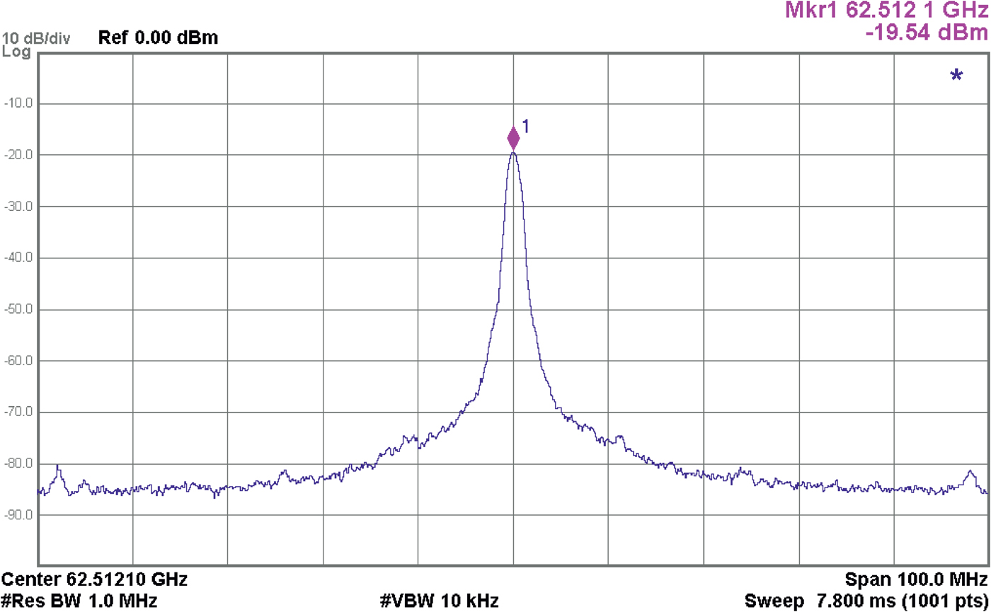
Fig. 11. Output spectrum of the VCO.
As can be seen in Fig. 11, the spectrum is clean. Additionally, Fig. 12 shows the spectrum for two values of the tuning voltage 0 and 1.1 V. The output frequency is tuned from 51.9 to 65.4 GHz. In case it is possible to tune the voltage beyond the supply of 1.1 V, the tuning range can be extended up to 67 GHz by tuning voltage up to 1.3 V.
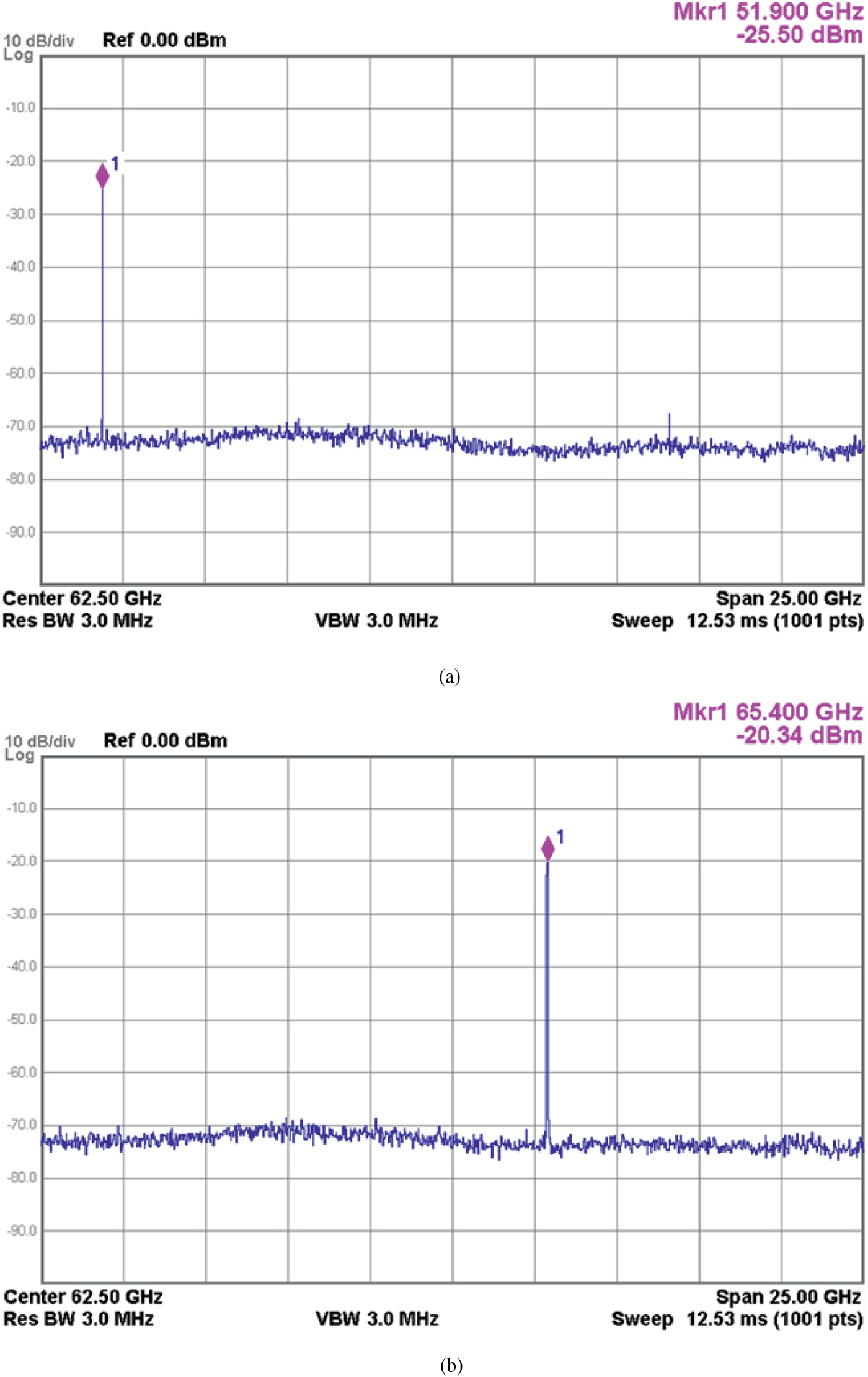
Fig. 12. Measured output spectrum for two values of tune voltage. (a) Vtune 0 V. (b) Vtune 1.1 V.
Furthermore, Fig. 13 shows the measured and simulated tuning characteristic of the VCO. The result is obtained by tuning both cores simultaneously. As can be seen, the VCO exhibits linear characteristics, providing little variation on K-VCO. This is very advantageous for easier design of a PLL. Some minor nonlinearity of tuning curve is observed in measurement. This could be due to insufficiently accurate models of the varactors.

Fig. 13. Measured and simulated tuning characteristics of the VCO.
The free-running phase noise measurement, performed at 62 GHz, is presented in Fig. 14. The phase noise level of −91.8 dBc/Hz at 1 MHz offset has been observed at the H2 output. This corresponds to a phase noise of −97.8 dBc/Hz at 1 MHz at the fundamental frequency. The measured result agrees reasonably well with the simulated value of −93.6 dBc/Hz at 62 GHz.

Fig. 14. Measured phase noise at 62 GHz.
The dual-core VCO including all the buffers turned on consumes 60 mA from a single 1.1 V supply. A single VCO core consumes 18 mA.
Conclusion
We have presented a continuously tunable dual-core push–push VCO in 40 nm CMOS suitable for FMCW radar applications. The VCO achieves a low phase noise of −91.8 dBc/Hz at 1 MHz offset from a 62 GHz carrier and provides at the same time a wide continuously tunable FTR of 25%. The VCO cores are realized as a cross-coupled LC-VCO. The second harmonic is collected in a non-invasive way using a transformer.
The measured results and comparison with the state-of-the-art are given in Table 1. The presented VCO compares favorable with the existing designs in terms of continuously tunable frequency range. Additionally, the table includes the figure of merit including tuning range  ${\rm FOM}_{\rm T}$ including the frequency tuning range, defined in [Reference Fanori and Andreani11] as
 $${\rm FO}{\rm M}_{\rm T} = {\rm {\cal L}}\{ \Delta f\} - 20\log \left( {\displaystyle{{\,f_0} \over {\Delta f}}\displaystyle{{{\rm FTR}} \over {10}}} \right) + 10\log \left( {\displaystyle{{{\rm P}_{{\rm dc}}} \over {{\rm 1\; mW}}}} \right).$$
Furthermore, a more thorough comparison with the state of the art and overview of the recently published VCOs is given in Fig. 15. The comparison also includes VCOs realized not only in CMOS, but also in SiGe HBT and SOI CMOS processes. The hollow symbols represent VCOs with switched elements in the resonant tank. Hence, the FTR is extended by digital tuning. Solid symbols represent VCOs exhibiting a continuous tuning. We distinguish between digitally tuned and continuously tuned VCOs for fairness – in a digitally tuned VCO, a smaller varactor can be used in the tank. Hence, it is easier to achieve a better phase noise. As can be seen, the proposed VCO offers the best phase noise value at 60 GHz among continuously tuned VCOs in a CMOS technology. Only HBT bipolar VCOs offer a better value and a digitally tuned CMOS VCO. Further, the proposed VCO achieves the best continuous tuning range among VCOs operating at 60 GHz and realized in a pure CMOS. Again, only SiGe HBT and SOI CMOS designs achieve a better continuous FTR.
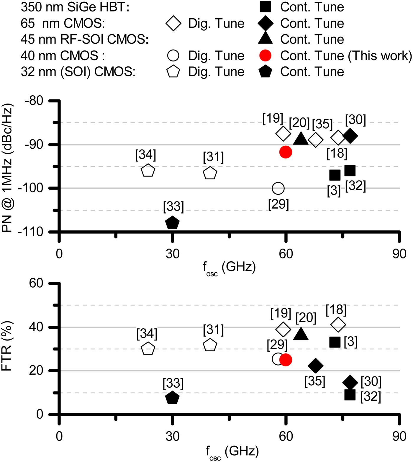
Fig. 15. Comparison with state of the art VCOs.
Table 1. Performance summary and comparison

aCannot be tuned continuously, while we tune continuously.
bGraphically estimated, as data for 1 MHz not available.
cComparison at 1 MHz offset from carrier.
 Vadim Issakov (Mʹ07- SMʹ16) was born in the Russian Federation in 1981. He received M.Sc. degree (cum laude) in microwave engineering from the Technical University of Munich and Ph.D. degree from the University of Paderborn, Germany (summa cum laude) in 2006 and 2010, respectively. He is a principal engineer for mm-wave circuit design at Infineon Technologies in Munich, Germany. He is a technical lead of a research group working on mm-wave circuit design in CMOS and SiGe technologies for radar, communication and industrial applications. His current research activities include highly integrated systems in CMOS and BiCMOS technologies at 60 GHz for backhaul communications, 60 GHz for gesture sensing radar, and 120 GHz radar for industrial applications.
Johannes Rimmelspacher received the EE Diploma degree from the University of Stuttgart majoring in integrated circuits. He is currently working towards a Ph.D. degree at the Institute for Electronics Engineering of Friedrich-Alexander-University Erlangen-Nuremberg in cooperation with Infineon Technologies. His research interests are in silicon-based mm-wave circuits.
 Saverio Trotta (Sʹ04-Mʹ07) was born in S. Giovanni R., Italy, in 1976. He received the Laurea degree in electronic engineering from Politecnico di Bari, Italy, and the Ph.D. degree from the TU Vienna, Austria, in 2003 and 2013, respectively. In 2003, he was with Fraunhofer institute, Erlangen-Nuremberg, Germany, where he was engaged in the development of high-speed digital ICs. From 2004 to 2007, he was with Infineon AG, Munich, Germany, where he was working on high frequency integrated circuit design beyond 100 GHz. From 2007 to 2011 he was with Freescale Semiconductor, developing chipsets for automotive radar applications at 77 GHz. Since 2011 he has been with Infineon AG, Munich, Germany, working in the field of communication systems in the V and E-band as well as 60 GHz radar-based gesture sensor systems.
 Marc Tiebout (Sʹ90-Mʹ93) was born in Asse, Belgium, in 1969. He received the M.Sc. degree in electrical and mechanical engineering in 1992 from the Katholieke Universiteit Leuven, Belgium, and the Ph.D. degree in electrical engineering from the Technical University of Berlin, Germany, in 2004. In 1993, he joined Siemens AG, Corporate Research and Development, Microelectronics in Munich, Germany, designing analog integrated circuits in CMOS and BiCMOS technologies. From 1999 to 2005, he was with Infineon Technologies AG, Munich, Germany, where he worked on RF-CMOS circuits and transceivers for cellular wireless communication products. Since 2006, he is with Infineon Technologies, Villach, Austria where his work includes Wimedia-UWB CMOS SoC development (system architect) and mm-Wave phased-array applications for radar, security and communications up to 80 GHz. He has authored and co-authored more than 100 IEEE publications and more than 45 patents.
 Amelie Hagelauer (Sʹ08-Mʹ10) was born in Nuremberg, Germany, in 1981. She received the Dipl.-Ing. degree in mechatronics and the Dr.-Ing. degree in electrical engineering from the Friedrich Alexander-University Erlangen-Nuremberg, Erlangen, Germany, in 2007 and 2013, respectively. She joined the Institute for Electronics Engineering of the Friedrich Alexander-University Erlangen-Nuremberg as a Research Engineer in 2007, where she is involved in where she is involved in SAW/BAW components, RF-MEMS, packaging technologies and integrated circuits up to 180 GHz. Dr. Hagelauer has been the Chair of MTT-2 Microwave Acoustics since 2015. Since 2016 she is leading a research group on Electronic Circuits.
 Robert Weigel (Fʹ02) received the Dr.-Ing. and the Dr.-Ing.habil. degrees, both in electrical engineering and computer science, from the Munich University of Technology in Germany where he respectively, was a Research Engineer, a Senior Research Engineer, and a Professor for RF Circuits and Systems until 1996. From 1996 to 2002, he has been Director of the Institute for Communications and Information Engineering at the University of Linz, Austria where, in August 1999, he co-founded the company DICE, devoted to the design of RFICs for mobile radio and MMICs for vehicular radar applications. Since 2002 he is Head of the Institute for Electronics Engineering at the University of Erlangen-Nuremberg, Germany. Prof. Weigel has published more than 900 papers on microwave theory and techniques, electronic circuits and systems, and communication and sensing systems.


