


I. INTRODUCTION
Recently, millimeter-wave applications have received considerable attention in various fields, such as high-speed wireless personal area networks (WPANs) using a 60 GHz band aimed at a wireless high-definition multimedia interface (HDMI) and an automotive radar using a 76 GHz band. In particular, a millimeter-wave-band transceiver with CMOS circuits is expected to realize a low-power operation that extends the battery duration and mobility in consumer electronic appliances. Here, in CMOS circuits, a differential topology is often adopted in analog and radio-frequency circuits. For example, power-supply noise is cancelled by a differential low-noise amplifier (LNA) and local oscillator (LO) leakage is also cancelled by a double balanced mixer [Reference Trifunovic and Jokanovic1, Reference Razavi2]. Additionally, in a large-signal operation, linearity is improved with a differential topology because second-harmonic signals are balanced out [Reference Razavi3]. On the other hand, off-chip devices in a millimeter wave band generally have single-end ports. Moreover, tests for single-end devices are much simpler than those for differential devices. To realize single-end devices using differential CMOS circuits while retaining these features, on-chip baluns are required.
Two types of millimeter-wave on-chip balun have been reported: rat-race balun [Reference Chirala and Floyd4–Reference Ng, Chongcheawchamnan and Robertson6] and Marchand balun [Reference Lai, Inui and Fujishima7–Reference Wu, Lin, Huang, Wang, Wang and Wu11]. Rat-race baluns realize a low insertion loss even with single-layer signal paths, since the electromagnetic coupling of two transmission lines, as required for Marchand baluns, is unnecessary, as shown in Fig. 1. However, rat-race baluns occupy a larger area than Marchand baluns because the total length of the transmission line of the rat race is 1.5 times the wavelength. To overcome this problem, a rewiring technology for fabricating a lead frame utilizing a wafer-level chip-size package (W-CSP) is adopted to form the rat-race balun in this study. The new balun requires no additional die area because devices fabricated by the W-CSP technology are placed over a chip. When the W-CSP balun is connected to differential CMOS circuits, differential ports should be connected through GSGSG pads, so that the CMOS circuits may be measured alone without connecting the W-CSP balun. To achieve this, the differential ports in the W-CSP balun should be aligned with the pads. Additionally, the area occupied by the balun should be small so as to be unobtrusive in the package lead frame. From these viewpoints, the form of conventional rat-race baluns is unsuitable for the W-CSP balun, because the differential ports are not aligned with the GSGSG pads even though the meandering structure may reduce the area. In this work, the newly proposed S-shaped structure with differential ports aligned with the GSGSG pads is used, and the meandering structure reduces the area. In the following sections, after the principle of the W-CSP S-shaped balun is explained, measurement results are discussed.

Fig. 1. (a) Rat-race balun realizes low-insertion loss even with single-layer single path. (b) Electromagnetic coupling of two transmission lines is required for the planar and stacked Marchand baluns.
II. S-SHAPED RAT-RACE BALUN USING W-CSP
A) W-CSP process for rat-race balun
A basic rat-race balun has four ports with a circular transmission line, as shown in Fig. 2. When the rat race is used for a balun, only three ports are used: single-end port 1 and two differential ports 2 and 4. The distances between the ports are proportional to the wavelength λ, and the total length of the circular transmission line is 3λ/2.
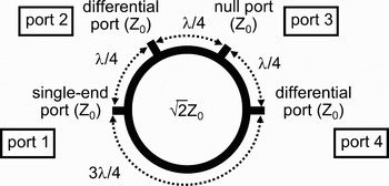
Fig. 2. Basic rat-race balun.
Because the rat-race balun requires only a single layer, other layers are freely utilized for the circuits, and the full chip area can be utilized effectively for the circuits by using the rewiring layer in the W-CSP. A single-layer W-CSP process is adopted in this study. A cross-sectional view of the W-CSP balun with CMOS circuits is shown in Fig. 3. W-CSP is originally used for packaging. It provides an interface between the CMOS chip and the off-chip environment. The top metal of the CMOS chip is connected to the rewiring metals of the W-CSP through aluminum pads, and then, the rewired layers of the W-CSP are connected to the off-chip environment by copper bumps and solder balls [Reference Garrou12]. Since the rewiring layer is made of a thick copper film on a thick polyimide insulator film, the loss of the transmission line and the effect of wiring of other layers are small because the thick insulator layer increases the distance between the lossy silicon substrate and the rewiring layer. The conductance of a transmission line is approximated by the multiplication of thickness, width, and skin depth. Since the skin depth decreases at millimeter-wave circuits where the skin effect of copper at 60 GHz is about 300 nm [Reference Hajimiri13], wider and thicker metals have less resistive loss. The thicknesses of the copper and polyimide films are both 5 µm in this design where thickness of the used metal is approximately five times larger than that of a typical metal line in a standard CMOS technology.

Fig. 3. Simplified cross-section of the W-CSP and CMOS process.
The top metal of the CMOS process is used as a ground shield to utilize the single-layer W-CSP process, as shown in Fig. 4. The W-CSP balun and CMOS circuits are decoupled by the ground shield. It is not a critical issue that the top metal is unavailable for wirings in the CMOS circuits because a small number of layers are used in the RF circuits. When two layers are available in the W-CSP process, the lower layer can be used as the ground shield, and all metal layers in the CMOS process are available. The coupling between the ground shield and the circuits must be considered in the design because the ground shield simultaneously works as the top ground of the CMOS circuits as well as the bottom ground of the W-CSP balun.

Fig. 4. Top metal is used as a ground shield.
A slow-wave transmission line (SWTL) [Reference Lai, Tanimoto and Fujishima14] is adopted as the transmission line in the W-CSP process in this study to improve the performance of the W-CSP balun. Figure 5 shows the structure of the SWTL. In the SWTL, the bottom ground shield has slits vertical to the signal line, which prevent return current from flowing through the bottom ground [Reference Inui, Manzawa and Fujishima15]. As a result, the inductance of the transmission line increases compared with that of a microstrip line without using slits, although capacitance remains approximately the same. Consequently, the wavelength of the transmission line decreases and the characteristic impedance of the transmission line increases, which lead to the enhancement of the performance of the balun. The effective dielectric constant is 1.6 times that of the microstrip line; therefore, the slowing factor is calculated to be 1.26 times that of the microstrip line. In the SWTL, signal lines and coplanar grounds are prepared using a rewiring layer in the W-CSP, and the ground shield under the signal line is formed using the top layer of the CMOS process [Reference Lai and Fujishima16].

Fig. 5. Structure of SWTL.
B) S-shaped rat-race balun
The differential ports in the rat-race balun are aligned so as to connect them directly to the GSGSG pads on the chip, as shown in Fig. 6(a). The pitch of the millimeter-wave GSGSG pads is 100 µm. In conventional on-chip rat-race baluns, although a meandering structure is often adopted for area reduction, the differential ports are not aligned with the GSGSG pads, as shown in Fig. 6(b). Since the terminal impedance of port 3 does not affect the performance of the balun [Reference Bex17], port 3 can be removed, and the rat race is deformed into an S shape to be aligned with the differential GSGSG pads, as shown in Fig. 7. Figure 7(a) shows the basic shape of the rat-race balun, where the space in the center of the circular transmission line occupies a large area. To remove the center space, the circular transmission line can be modified into a parallel straight transmission line, as shown in Fig. 7(b). The removal of port 3 renders the shape of the rat race flexible. With ports 2 and 4 placed close to each other, when the parallel straight line is folded, the rat race becomes S-shaped, as shown in Fig. 7(c). As a result, the core size of the S-shaped rat-race balun becomes 22.4% that of the square rat-race balun.
Fig. 6. (a) Balun with differential ports aligned with the GSGSG pads can be connected to the chip directly, but (b) conventional balun cannot be connected directly to the GSGSG pads.

Fig. 7. (a) The basic structure of the rat race is circular. (b) The rat race is flattened to remove the center space. (c) The flattened rat race is folded to align the differential ports to the GSGSG pads.
III. DESIGN AND MEASUREMENTS
Based on the concept explained in the previous section, a millimeter-wave S-shaped rat-race balun is fabricated using the rewiring technology of the W-CSP on a 0.15 µm silicon-on-insulator (SOI)-CMOS substrate. Figure 8 shows a micrograph of the fabricated chip. The core size without pads is 480 × 735 µm. Since the terminal impedance of port 3 does not affect the performance of the balun [Reference Bex17], port 3 is kept open. Neighboring signal lines are decoupled by coplanar ground shields.

Fig. 8. Micrograph of the proposed balun.
A) Design of the transmission line and measurement results
As explained in the previous section, a SWTL is adopted for the S-shaped W-CSP balun. In the rat-race balun, the characteristic impedance of the transmission line Z 0 is typically chosen as ![]() times of the terminal impedance Z L at each port. The return loss at each port increases when Z 0 is different from
times of the terminal impedance Z L at each port. The return loss at each port increases when Z 0 is different from ![]() , which is 70.7 Ω in the 50 Ω system. Although a single-end port is directly connected to an external 50 Ω load, the differential ports are connected to the CMOS circuits through a matching circuit, as shown in Fig. 9, where the optimum impedances at ports 2 and 4 are equal to one over a square root of two times the transmission line characteristic impedance. Because of the matching circuit, the characteristic impedance may be different from 70.7 Ω, as long as the return loss at the single-end port is in an acceptable range.
, which is 70.7 Ω in the 50 Ω system. Although a single-end port is directly connected to an external 50 Ω load, the differential ports are connected to the CMOS circuits through a matching circuit, as shown in Fig. 9, where the optimum impedances at ports 2 and 4 are equal to one over a square root of two times the transmission line characteristic impedance. Because of the matching circuit, the characteristic impedance may be different from 70.7 Ω, as long as the return loss at the single-end port is in an acceptable range.

Fig. 9. S11 in 50 Ω system is important because the single-end port is directly connected to 50 Ω load. In contrast, S22 and S44 are not important because there are matching circuit between differential port and circuits.
The characteristic impedance and transmission loss of the SWTL are determined using the width of the signal line and the space between the signal line and the coplanar ground. Furthermore, when the occupied area is fixed, a trade-off is observed between the width of the signal line and the space between the signal line and the coplanar ground. Thus, the characteristic impedance and attenuation constant of the transmission line when the space between the inner edges of the coplanar grounds is fixed at 55 µm are calculated as a function of signal linewidth. Each value is calculated using equations in [Reference Wu, Lin, Huang, Wang, Wang and Wu11] using a process parameter. Calculated results are shown in Fig. 10, which indicates that a narrower signal line is required to increase the characteristic impedance of the transmission line. In contrast, to reduce the loss of the transmission line without an increase in occupied area, a wider signal line is necessary. Therefore, a trade-off is observed between the transmission loss and characteristic impedance of the transmission line. In this study, under the condition that the return loss at the single-end port is less than −10 dB, the characteristic impedance of the transmission line was chosen as approximately 50 Ω. To achieve this characteristic impedance, the width of the SWTL was chosen as 15 µm and the space between the signal line and the coplanar ground was chosen as 20 µm.

Fig. 10. Calculated characteristic impedance and attenuation constant of the SWTL as a function of the width of signal line when distance between coplanar grounds is fixed.
From the measurement results for the transmission line, the characteristic impedance, transmission loss, and phase constant at 50 GHz are 52.5 Ω, 0.5 dB/mm, and 115 degrees/mm, respectively, as shown in Fig. 10. Owing to the thick and wide metal of the W-CSP process, the transmission loss is smaller than that of the transmission lines fabricated by most CMOS technologies [Reference Cathelin18]. It is noted that the measurement results agree in the cases of a high-resistivity substrate and a low-resistivity substrate, owing to the presence of the ground shield.
B) Measurement result for the fabricated S-shaped rat-race balun
Three different fabricated chips were measured by a four-port vector network analyzer (VNA). After ensuring that the results of measurements are the same, one of the obtained data were evaluated. The pads and lead lines of the balun were de-embedded using the de-embedding method in [Reference Goto, Natsukari and Fujishima19], which has an approximately 1.2% error. The real part of the characteristic impedance, attenuation constant, and phase constant of the transmission line is shown in Fig. 11. Since the characteristic impedance of the fabricated transmission line is measured to be 52.5 Ω, the optimum terminal impedances at ports 1, 2, and 4 are calculated to be 37 Ω. Figure 12(a) shows the return loss at each port in the 50 Ω terminal. For comparison, the return loss in the 37 Ω terminal, which is ![]() , is also shown in Fig. 12(b). Figure 12 indicates that S11 is less than −10 dB, although all the return losses in the case of 50 Ω terminal impedance are degraded compared with those in the case of 37 Ω terminal impedance. Figure 13 shows the amplitude and phase imbalances between the differential ports with the 50 Ω terminal to be ±1.5 dB and ±15° at operating frequencies from 40 to 61 GHz, respectively. These values guarantee the normal operation of the balun. Figure 14 shows the differential-mode gain G diff and common-mode gain G com of the fabricated balun in the 50 Ω system. Here, G diff and G com are obtained as
, is also shown in Fig. 12(b). Figure 12 indicates that S11 is less than −10 dB, although all the return losses in the case of 50 Ω terminal impedance are degraded compared with those in the case of 37 Ω terminal impedance. Figure 13 shows the amplitude and phase imbalances between the differential ports with the 50 Ω terminal to be ±1.5 dB and ±15° at operating frequencies from 40 to 61 GHz, respectively. These values guarantee the normal operation of the balun. Figure 14 shows the differential-mode gain G diff and common-mode gain G com of the fabricated balun in the 50 Ω system. Here, G diff and G com are obtained as
and

Fig. 11. Measured results of (a) real part of the characteristic impedance Z 0, (b) attenuation constants of the transmission line, and (c) phase constant of the transmission line.

Fig. 12. Comparison between the return losses of the proposed balun terminated by (a) 50 Ω loads and (b) 37 Ω loads.

Fig. 13. (a) The amplitude and (b) the phase imbalances of the proposed balun terminated by 50 Ω loads.

Fig. 14. The differential-mode gain and the common-mode gain of proposed balun terminated by 50 Ω loads.
G diff represents the signal penetration with conversion from single-end signals to differential signals [Reference Bockelman and Eisenstadt20]. In the case of a passive balun, since G diff theoretically becomes 0 dB, the insertion loss of the balun is estimated using G diff. On the other hand, G com indicates the signal leakage without conversion from single-end signals to differential signals. The measured insertion loss ranges from 1.4 to 3.7 dB at operating frequencies from 40 to 61 GHz. Since G com is below −19 dB at the operating frequency, it is concluded that no side effects of the removal of port 3 are observed. A weak resonance at 42 GHz was observed; this resonance was probably due to permanent parasitic between circuit and probe connections. However, it is not considered hazardous since it is in the off-band and has more than a 20 dB attenuation.
It is difficult to obtain low-loss passive devices inside the CMOS, because the performance of these devices in the CMOS depends on the technology. Typically, advanced CMOS technology requires very strict metallization design rules and strict density rules that do not allow designers to realize all desired widths and spacings; additionally, not all CMOS processes have thick metal layers for realizing low-loss devices. Figure 15 shows minimum insertion losses as a function of operating frequency for various on-chip baluns. The minimum insertion loss of the proposed balun is the smallest among those of other millimeter-wave baluns.

Fig. 15. Minimum insertion losses of the proposed and other millimeter-wave on-chip baluns.
IV. CONCLUSION
The rewiring technology of a W-CSP was applied to a rat-race balun to suppress the area penalty. To overcome the alignment problem of differential GSGSG pads on a chip, an S-shaped rat-race balun is proposed. The proposed S-shaped rat-race balun not only reduces chip area but also is connected directly to the differential GSGSG pads. The core size of the S-shaped rat-race balun becomes 22.4% that of a square rat-race balun. The S-shaped rat-race balun was fabricated using the W-CSP technology on a 0.15 µm SOI-CMOS substrate. From measurement results, it was found that the minimum insertion loss is 1.7 dB. The operating frequency ranges from 40 to 61 GHz when the amplitude and phase imbalances between the differential ports are ±1.5 dB and ±15°, respectively, and the insertion loss ranges from 1.4 to 3.7 dB with a 50 Ω terminal. The adoption of the proposed S-shaped rat-race balun using the W-CSP can eliminate the need for an additional area between on-chip differential and off-chip single-end circuits. When the proposed balun is adopted, device integration is expected to be improved in millimeter-wave CMOS circuits, which is expected to contribute to the low-cost 60 GHz short-range high-speed wireless transmission used for a wireless HDMI and a 76 GHz automotive radar.
ACKNOWLEDGEMENTS
This study is supported by the joint research project with the Semiconductor Technology Academic Research Center (STARC). The authors would like to thank Mr. Tani and Mr. Terui of OKI Electric Industry Co., Ltd. for chip fabrication.
 Ahmet Oncu received the B.S. degree in physics and the B.S. degree in electrical and electronics engineering from Middle East Technical University (METU), Ankara, Turkey, in 2001 and 2002, respectively. He received the M.S. degree in microwave engineering from the Technical University of Munich, Germany, in 2004. He received the Ph.D. degree from the University of Tokyo, Japan, in September 2008. He is currently a post-doctoral research associate at the Department of Electrical Engineering and Information Systems, the University of Tokyo. His research interests are in designs of millimeter-wave CMOS circuits for 60 GHz Wireless HDMI.
 Chiaki Inui received the B.E. degree in applied physics from WASEDA University in Tokyo in 2005 and M.S. degree in frontier informatics from the University of Tokyo in 2008. His research interest is design of LNA, balun, and transmission lines in millimeter-wave CMOS circuits. Currently he is working at Softbank Mobile Corporation.
 Yasuo Manzawa received the B.E. degree in electrical engineering and M.S. degree in frontier informatics from the University of Tokyo, Japan, in 2007 and 2009, respectively. His research interests are the design methodology and design automation of millimeter-wave CMOS circuits. Currently he is working at Keyence Corporation.
 Minoru Fujishima received the B.E., M.E., and Ph.D. degrees in electronics engineering from the University of Tokyo, Japan, in 1988, 1990, and 1993, respectively. He joined the faculty of the University of Tokyo in 1988 as a Research Associate, and is currently an Associate Professor of the School of Frontier Sciences, University of Tokyo. He was a visiting Professor at the ESAT-MICAS Laboratory, Katholieke, Universiteit Leuven, Belgium, from 1998 to 2000. His interests are in design and modeling of millimeter-wave CMOS circuits for wireless transceiver era of sub-100 nm technology.


